


Parylene-AlOx Stacks for Improved 3D Encapsulation Solutions

 ,
,  , and
, and
Abstract
: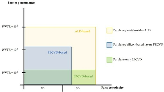
1. Introduction
2. Materials and Methods
2.1. Substrate
2.1.1. PET Melinex PCS Grade Substrate
2.1.2. PI Kapton HN Grade Substrate
2.2. Inorganic Layer Deposition
2.2.1. PECVD Silicon Oxide, SiOx
2.2.2. PECVD Silicon Nitride, SiNx
2.2.3. ALD Metal Oxides
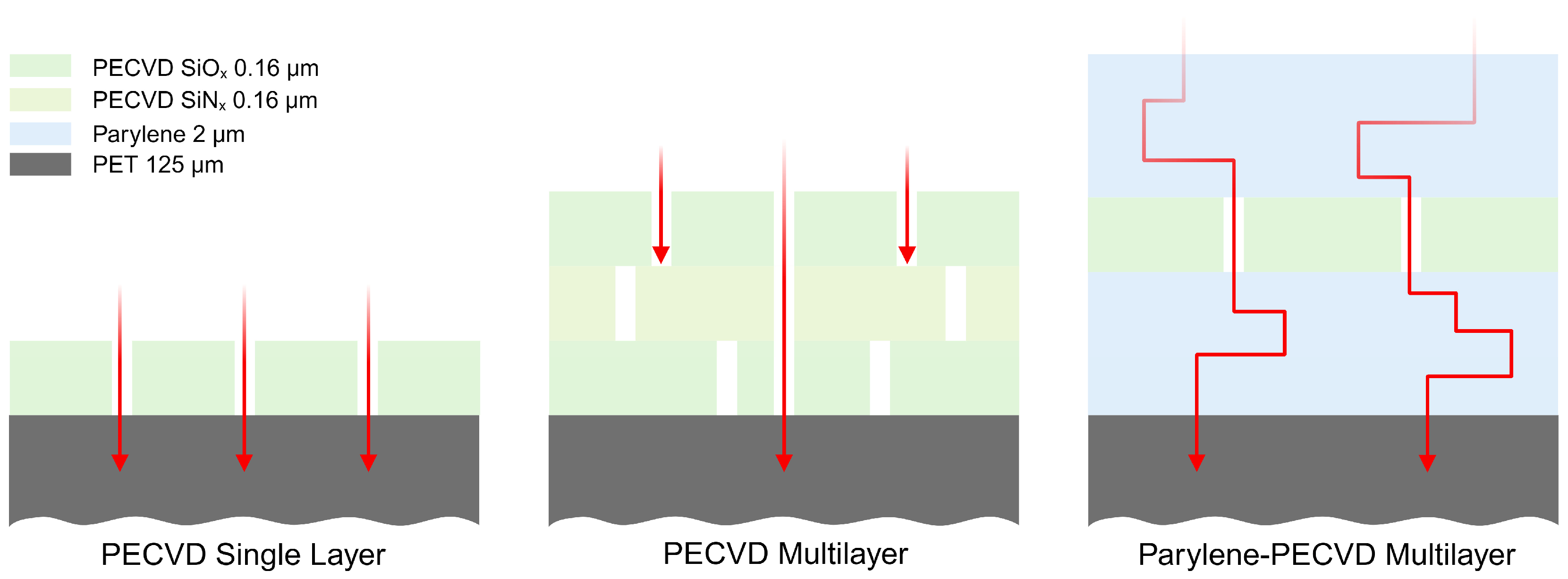
2.3. Organic Layer Deposition
2.4. Characterization Method
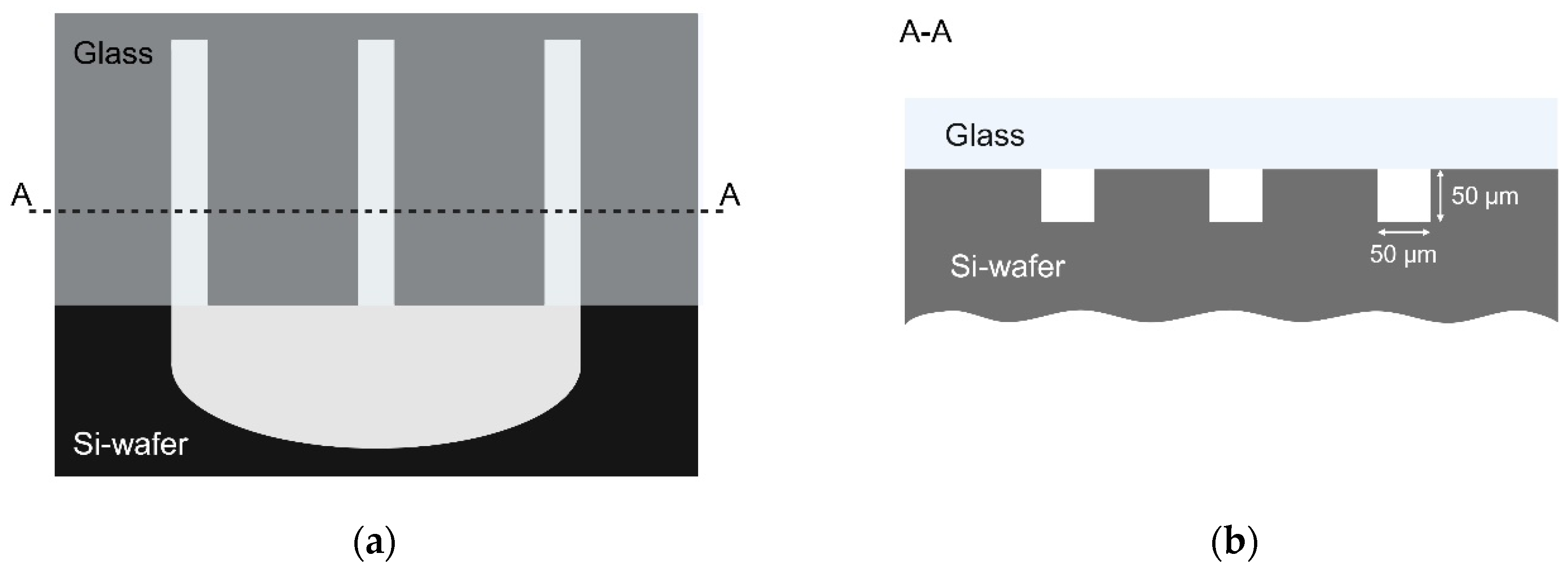
2.4.1. Conformality Investigation
2.4.2. WVTR Electrolytic Detection Method
2.4.3. WVTR Diode Laser Spectroscopy Method
3. Results and Discussion
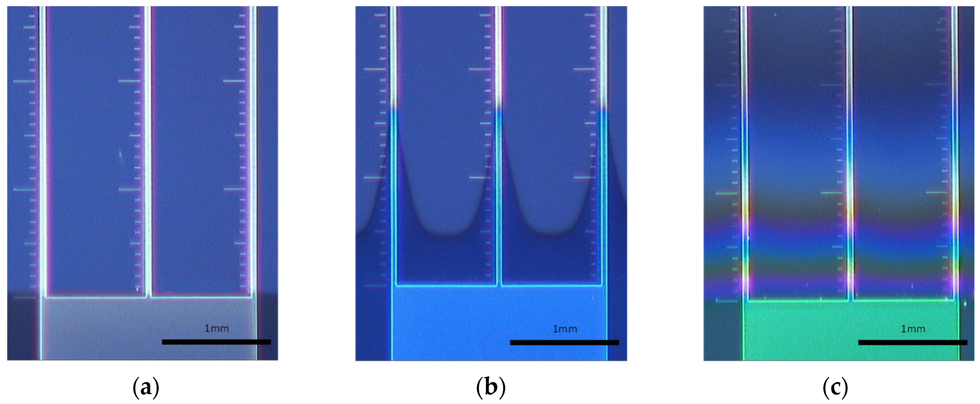
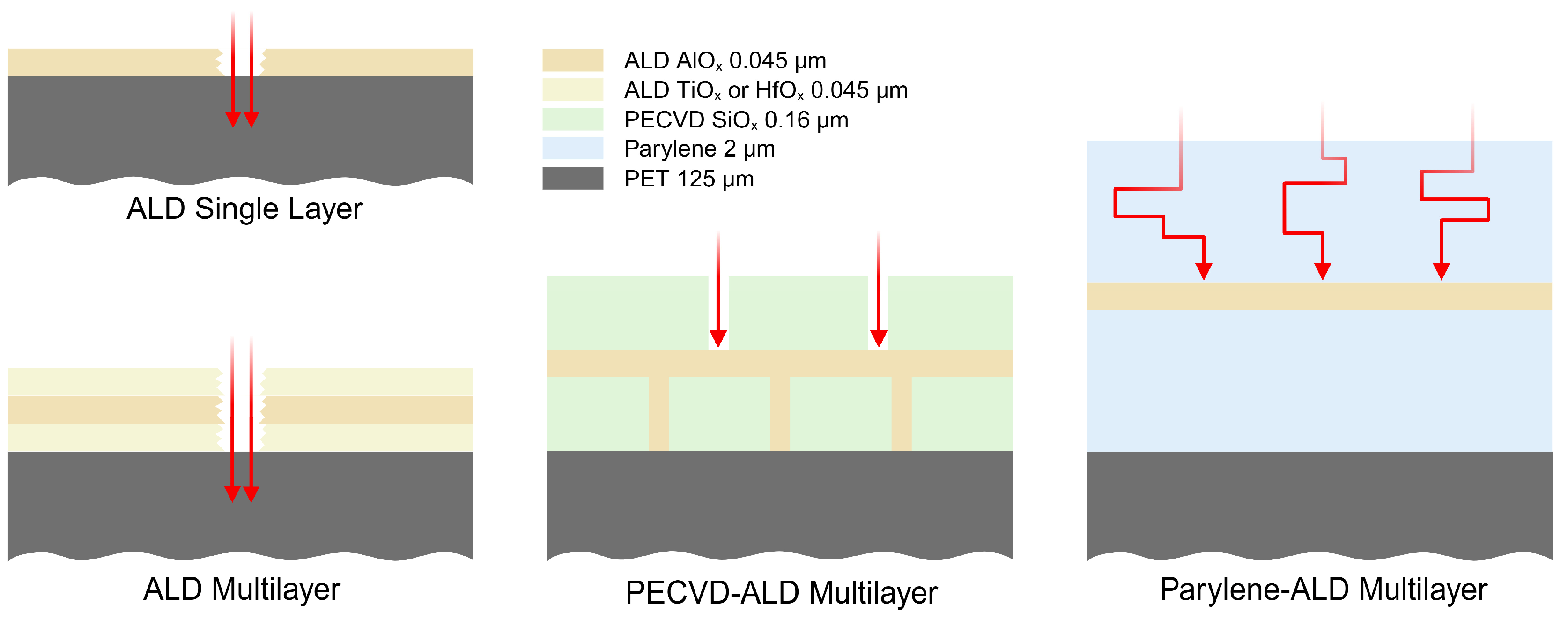
3.1. Conformality
3.2. PECVD SiOx and SiNx Barrier Layers
3.3. ALD Metal Oxide Barrier Layers
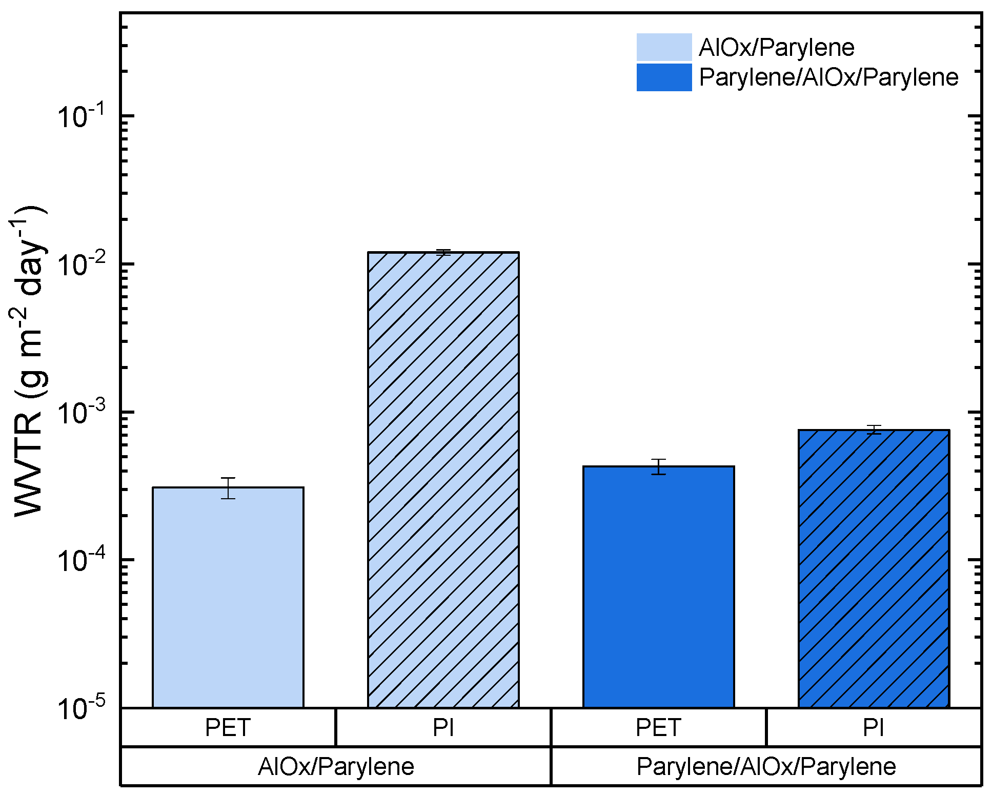
3.3.1. WVTR Results on PET Melinex PCS Substrate
3.3.2. WVTR Results on PI Kapton HN Substrate
4. Conclusions
Author Contributions
Funding
Institutional Review Board Statement
Informed Consent Statement
Data Availability Statement
Acknowledgments
Conflicts of Interest
Appendix A

References
- Gorham, W.F. A New, General Synthetic Method for the Preparation of Linear Poly-p-Xylylenes. J. Polym. Sci. Part A-1 Polym. Chem. 1966, 4, 3027–3039. [Google Scholar] [CrossRef]
- Baschetti, M.G.; Minelli, M. Test Methods for the Characterization of Gas and Vapor Permeability in Polymers for Food Packaging Application: A Review. Polym. Test. 2020, 89, 106606. [Google Scholar] [CrossRef]
- ISO 15106; Plastics—Film and Sheeting—Determination of Water Vapour Transmission Rate. ISO: Geneva, Switzerland, 2003.
- Nisato, G.; Bouten, P.C.; Slikkerveer, P.J.; Bennet, W.D.; Graff, G.L.; Rutherford, N.; Wiese, L. Evaluationg High Performance Diffusion Berriers. In Proceedings of the 21st Annual Asia Display, 8th International Display Workshops, Singapore, 2001; p. 1435. [Google Scholar]
- Beese, H.; Grählert, W.; Kaskel, S.; Grübler, J.; Koch, J.; Pietsch, K. HiBarSens: Measurement of Barrier Properties by Tunable Diode Laser Absorption Spectroscopy (TDLAS). In Proceedings of the 2012 Web Coating & Handling Conference of the Association of Industrial Metallizers, Coaters and Laminators AIMCAL, Myrtle Beach, SC, USA, 21–24 October 2012; p. 848, ISBN 978-1-622-76950-6. [Google Scholar]
- Lee, S.; Han, J.H.; Lee, S.H.; Baek, G.H.; Park, J.S. Review of Organic/Inorganic Thin Film Encapsulation by Atomic Layer Deposition for a Flexible OLED Display. JOM 2019, 71, 197–211. [Google Scholar] [CrossRef]
- Nehm, F.; Dollinger, F.; Klumbies, H.; Müller-Meskamp, L.; Leo, K.; Singh, A.; Richter, C.; Schroeder, U.; Mikolajick, T.; Hossbach, C.; et al. Atomic Layer Deposited TiOx/AlOx Nanolaminates as Moisture Barriers for Organic Devices. Org. Electron. 2016, 38, 84–88. [Google Scholar] [CrossRef]
- Kim, B.J.; Meng, E. Micromachining of Parylene C for BioMEMS. Polym. Adv. Technol. 2016, 27, 564–576. [Google Scholar] [CrossRef]
- Andringa, A.M.; Perrotta, A.; De Peuter, K.; Knoops, H.C.M.; Kessels, W.M.M.; Creatore, M. Low-Temperature Plasma-Assisted Atomic Layer Deposition of Silicon Nitride Moisture Permeation Barrier Layers. ACS Appl. Mater. Interfaces 2015, 7, 22525–22532. [Google Scholar] [CrossRef] [PubMed]
- Kim, J.; Ghaffari, R.; Kim, D.-H. The Quest for Miniaturized Soft Bioelectronic Devices. Nat. Biomed. Eng. 2017, 1, 49. [Google Scholar] [CrossRef]
- Bülow, T.; Gargouri, H.; Siebert, M.; Rudolph, R.; Johannes, H.H.; Kowalsky, W. Moisture Barrier Properties of Thin Organic-Inorganic Multilayers Prepared by Plasma-Enhanced ALD and CVD in One Reactor. Nanoscale Res. Lett. 2014, 9, 223. [Google Scholar] [CrossRef]
- Jackson, N.; Olszewski, O.Z.; O’Murchu, C.; Mathewson, A. Ultralow-Frequency PiezoMEMS Energy Harvester Using Thin-Film Silicon and Parylene Substrates. J. Micro/Nanolithography MEMS MOEMS 2018, 17, 015005. [Google Scholar] [CrossRef]
- Lagomarsini, C.; Jean-Mistral, C.; Kachroudi, A.; Monfray, S.; Sylvestre, A. Outstanding Performance of Parylene Polymers as Electrets for Energy Harvesting and High-Temperature Applications. J. Appl. Polym. Sci. 2020, 137, 48790. [Google Scholar] [CrossRef]
- Lo, H.W.; Tai, Y.C. Parylene-HT-Based Electret Rotor Generator. In Proceedings of the 2008 IEEE 21st International Conference on Micro Electro Mechanical Systems, Tucson, AZ, USA, 13–17 January 2008; pp. 984–987. [Google Scholar] [CrossRef]
- Marquardt, K.; Hahn, R.; Luger, T.; Reichl, H. Thin Film Encapsulation for Secondary Batteries on Wafer Level. In Proceedings of the 2006 1st Electronic Systemintegration Technology Conference, Dresden, Germany, 5–7 September 2006; Volume 2, pp. 1410–1416. [Google Scholar]
- Lee, H.; Lim, K.Y.; Kim, K.-B.; Yu, J.-W.; Choi, W.K.; Choi, J.-W. Hybrid Thin-Film Encapsulation for All-Solid-State Thin-Film Batteries. ACS Appl. Mater. Interfaces 2020, 12, 11504–11510. [Google Scholar] [CrossRef] [PubMed]
- Cros, S.; de Bettignies, R.; Berson, S.; Bailly, S.; Maisse, P.; Lemaitre, N.; Guillerez, S. Definition of Encapsulation Barrier Requirements: A Method Applied to Organic Solar Cells. Sol. Energy Mater. Sol. Cells 2011, 95, S65–S69. [Google Scholar] [CrossRef]
- Xie, X.; Rieth, L.; Caldwell, R.; Diwekar, M.; Tathireddy, P.; Sharma, R.; Solzbacher, F. Long-Term Bilayer Encapsulation Performance of Atomic Layer Deposited Al2O3 and Parylene c for Biomedical Implantable Devices. IEEE Trans. Biomed. Eng. 2013, 60, 2943–2951. [Google Scholar] [CrossRef] [PubMed]
- Hogg, A.; Uhl, S.; Feuvrier, F.; Girardet, Y.; Graf, B.; Aellen, T.; Keppner, H.; Tardy, Y.; Burger, J. Protective Multilayer Packaging for Long-Term Implantable Medical Devices. Surf. Coat. Technol. 2014, 255, 124–129. [Google Scholar] [CrossRef]
- Lacour, S.P.; Benmerah, S.; Tarte, E.; FitzGerald, J.; Serra, J.; McMahon, S.; Fawcett, J.; Graudejus, O.; Yu, Z.; Morrison, B. Flexible and Stretchable Micro-Electrodes for in Vitro and in Vivo Neural Interfaces. Med. Biol. Eng. Comput. 2010, 48, 945–954. [Google Scholar] [CrossRef] [PubMed]
- Park, H.; Choi, W.; Oh, S.; Kim, Y.-J.; Seok, S.; Kim, J. A Study on Biocompatible Polymer-Based Packaging of Neural Interface for Chronic Implantation. Micromachines 2022, 13, 516. [Google Scholar] [CrossRef] [PubMed]
- Fahlteich, J.; Top, M.; Hinze, S.; Meyer, U.; Vogt, T.; von Morgen, V.; Fahland, M. Roll-to-Roll Processing of Transparent and Robust Permeation Barrier Films for Flexible Electronics. Proc. Int. Disp. Work. 2019, 3, 1570–1573. [Google Scholar] [CrossRef]
- Lua, A.C.; Su, J. Isothermal and Non-Isothermal Pyrolysis Kinetics of Kapton® Polyimide. Polym. Degrad. Stab. 2006, 91, 144–153. [Google Scholar] [CrossRef]
- Buchwalder, S.; Borzì, A.; Diaz Leon, J.J.; Bourgeois, F.; Nicolier, C.; Nicolay, S.; Neels, A.; Zywitzki, O.; Hogg, A.; Burger, J. Thermal Analysis of Parylene Thin Films for Barrier Layer Applications. Polymers 2022, 14, 3677. [Google Scholar] [CrossRef]
- Jackson, N.; Stam, F.; O’Brien, J.; Kailas, L.; Mathewson, A.; O’Murchu, C. Crystallinity and Mechanical Effects from Annealing Parylene Thin Films. Thin Solid Films 2016, 603, 371–376. [Google Scholar] [CrossRef]
- Beach, W.F. A Model for the Vapor Deposition Polymerization of P-Xylylene. Macromolecules 1978, 11, 72–76. [Google Scholar] [CrossRef]
- Kahouli, A.; Sylvestre, A.; Laithier, J.F.; Lutsen, L.; Pairis, S.; André, E.; Garden, J.L. Structural and Dielectric Properties of Parylene-VT4 Thin Films. Mater. Chem. Phys. 2014, 143, 908–914. [Google Scholar] [CrossRef]
- Senkevich, J.J.; Desu, S.B.; Simkovic, V. Temperature Studies of Optical Birefringence and X-ray Diffraction with Poly(p-Xylylene), Poly(Chloro-p-Xylylene) and Poly(Tetrafluoro-p-Xylylene) CVD Thin Films. Polymer 2000, 41, 2379–2390. [Google Scholar] [CrossRef]
- Mizuno, S.; Verma, A.; Lee, P.; Nguyen, B. Improved Gap-Filling Capability of Fluorine-Doped PECVD Silicon Oxide Thin Films. Thin Solid Films 1996, 279, 82–86. [Google Scholar] [CrossRef]
- Archard, D.; Giles, K.; Price, A.; Burgess, S.; Buchanan, K. Low Temperature PECVD of Dielectric Films for TSV Applications. In Proceedings of the 2010 Proceedings 60th Electronic Components and Technology Conference (ECTC), Las Vegas, NV, USA, 1–4 June 2010; pp. 764–768. [Google Scholar]
- Gabriel, N.T.; Talghader, J.J. Optical Coatings in Microscale Channels by Atomic Layer Deposition. Appl. Opt. 2010, 49, 1242–1248. [Google Scholar] [CrossRef]
- Gao, F.; Arpiainen, S.; Puurunen, R.L. Microscopic Silicon-Based Lateral High-Aspect-Ratio Structures for Thin Film Conformality Analysis. J. Vac. Sci. Technol. A 2014, 33, 10601. [Google Scholar] [CrossRef]
- Cremers, V.; Puurunen, R.L.; Dendooven, J. Conformality in Atomic Layer Deposition: Current Status Overview of Analysis and Modelling. Appl. Phys. Rev. 2019, 6, 21302. [Google Scholar] [CrossRef]
- Yim, J.; Ylivaara, O.M.E.; Ylilammi, M.; Korpelainen, V.; Haimi, E.; Verkama, E.; Utriainen, M.; Puurunen, R.L. Saturation Profile Based Conformality Analysis for Atomic Layer Deposition: Aluminum Oxide in Lateral High-Aspect-Ratio Channels. Phys. Chem. Chem. Phys. 2020, 22, 23107–23120. [Google Scholar] [CrossRef]
- Chen, P.-J.; Rodger, D.C.; Humayun, M.S.; Tai, Y.-C. Unpowered Spiral-Tube Parylene Pressure Sensor for Intraocular Pressure Sensing. Sens. Actuators A Phys. 2006, 127, 276–282. [Google Scholar] [CrossRef]
- Zoumpoulidis, T.; Bartek, M.; de Graaf, P.; Dekker, R. High-Aspect-Ratio through-Wafer Parylene Beams for Stretchable Silicon Electronics. Sens. Actuators A Phys. 2009, 156, 257–264. [Google Scholar] [CrossRef]
- Selvarasah, S.; Chao, S.H.; Chen, C.-L.; Sridhar, S.; Busnaina, A.; Khademhosseini, A.; Dokmeci, M.R. A Reusable High Aspect Ratio Parylene-C Shadow Mask Technology for Diverse Micropatterning Applications. Sens. Actuators A Phys. 2008, 145–146, 306–315. [Google Scholar] [CrossRef]
- Suzuki, Y.S.; Tai, Y.-C. Micromachined High-Aspect-Ratio Parylene Spring and Its Application to Low-Frequency Accelerometers. J. Microelectromechanical Syst. 2006, 15, 1364–1370. [Google Scholar] [CrossRef]
- Desai, C.; Laube, N. Development of a Technical Approach to Modify the Internal Surface of Biomedical Tubes and Other Elongated Small Lumen Macrodevices with Parylene Coating. J. Coatings Technol. Res. 2019, 16, 103–111. [Google Scholar] [CrossRef]
- Tropsha, Y.G.; Harvey, N.G. Activated Rate Theory Treatment of Oxygen and Water Transport through Silicon Oxide/Poly(Ethylene Terephthalate) Composite Barrier Structures. J. Phys. Chem. B 1997, 101, 2259–2266. [Google Scholar] [CrossRef]
- da Silva Sobrinho, A.S.; Czeremuszkin, G.; Latrèche, M.; Dennler, G.; Wertheimer, M.R. A Study of Defects in Ultra-Thin Transparent Coatings on Polymers. Surf. Coat. Technol. 1999, 116–119, 1204–1210. [Google Scholar] [CrossRef]
- Charifou, R.; Espuche, E.; Gouanvé, F.; Dubost, L.; Monaco, B. SiOx and SiOxCzHw Mono- and Multi-Layer Deposits for Improved Polymer Oxygen and Water Vapor Barrier Properties. J. Memb. Sci. 2016, 500, 245–254. [Google Scholar] [CrossRef]
- Triyoso, D.H.; Hempel, K.; Ohsiek, S.; Jaschke, V.; Shu, J.; Mutas, S.; Dittmar, K.; Schaeffer, J.; Utess, D.; Lenski, M. Evaluation of Low Temperature Silicon Nitride Spacer for High-k Metal Gate Integration. ECS J. Solid State Sci. Technol. 2013, 2, N222. [Google Scholar] [CrossRef]
- Chen, K.-S.; Tsai, Y.-G.; Yang, T.-H. Stress Analysis and Characterization of PECVD Oxide/Nitride Multi-Layered Films after Thermal Cycling. IEEE Trans. Device Mater. Reliab. 2021, 21, 17–25. [Google Scholar] [CrossRef]
- Kim, K.; Van Gompel, M.; Wu, K.; Schiavone, G.; Carron, J.; Bourgeois, F.; Lacour, S.P.; Leterrier, Y. Extended Barrier Lifetime of Partially Cracked Organic/Inorganic Multilayers for Compliant Implantable Electronics. Small 2021, 17, 2103039. [Google Scholar] [CrossRef]
- Dameron, A.A.; Davidson, S.D.; Burton, B.B.; Carcia, P.F.; McLean, R.S.; George, S.M. Gas Diffusion Barriers on Polymers Using Multilayers Fabricated by Al2O3 and Rapid SiO2 Atomic Layer Deposition. J. Phys. Chem. C 2008, 112, 4573–4580. [Google Scholar] [CrossRef]
- Fortin, J.B.; Lu, T.-M. Chemical Vapor Deposition Polymerization The Growth and Properties of Parylene Thin Films, 1st ed.; Springer: New York, NY, USA, 2004; ISBN 978-1-4020-7688-6. [Google Scholar]
- Ortigoza-Diaz, J.; Scholten, K.; Larson, C.; Cobo, A.; Hudson, T.; Yoo, J.; Baldwin, A.; Hirschberg, A.W.; Meng, E. Techniques and Considerations in the Microfabrication of Parylene C Microelectromechanical Systems. Micromachines 2018, 9, 422. [Google Scholar] [CrossRef]
- Li, C.; Cauwe, M.; Yang, Y.; Schaubroeck, D.; Mader, L.; Op de Beeck, M. Ultra-Long-Term Reliable Encapsulation Using an Atomic Layer Deposited HfO2/Al2O3/HfO2 Triple-Interlayer for Biomedical Implants. Coatings 2019, 9, 579. [Google Scholar] [CrossRef]
- Abdulagatov, A.I.; Yan, Y.; Cooper, J.R.; Zhang, Y.; Gibbs, Z.M.; Cavanagh, A.S.; Yang, R.G.; Lee, Y.C.; George, S.M. Al2O3 and TiO2 Atomic Layer Deposition on Copper for Water Corrosion Resistance. ACS Appl. Mater. Interfaces 2011, 3, 4593–4601. [Google Scholar] [CrossRef]
- Kim, L.H.; Jang, J.H.; Jeong, Y.J.; Kim, K.; Baek, Y.; Kwon, H.; An, T.K.; Nam, S.; Kim, S.H.; Jang, J.; et al. Highly-Impermeable Al2O3/HfO2 Moisture Barrier Films Grown by Low-Temperature Plasma-Enhanced Atomic Layer Deposition. Org. Electron. 2017, 50, 296–303. [Google Scholar] [CrossRef]
- Daubert, J.S.; Hill, G.T.; Gotsch, H.N.; Gremaud, A.P.; Ovental, J.S.; Williams, P.S.; Oldham, C.J.; Parsons, G.N. Corrosion Protection of Copper Using Al2O3, TiO2, ZnO, HfO2, and ZrO2 Atomic Layer Deposition. ACS Appl. Mater. Interfaces 2017, 9, 4192–4201. [Google Scholar] [CrossRef]
- Elers, K.; Blomberg, T.; Peussa, M.; Aitchison, B.; Haukka, S.; Marcus, S. Film Uniformity in Atomic Layer Deposition. Chem. Vap. Depos. 2006, 12, 13–24. [Google Scholar] [CrossRef]
- Van Hemmen, J.L.; Heil, S.B.S.; Klootwijk, J.H.; Roozeboom, F.; Hodson, C.J.; Van de Sanden, M.C.M.; Kessels, W.M.M. Plasma and Thermal ALD of Al2O3 in a Commercial 200 Mm ALD Reactor. J. Electrochem. Soc. 2007, 154, G165. [Google Scholar] [CrossRef]
- Verlaan, V.; van den Elzen, L.R.J.G.; Dingemans, G.; van de Sanden, M.C.M.; Kessels, W.M.M. Composition and Bonding Structure of Plasma-Assisted ALD Al2O3 Films. Phys. Status Solidi C 2010, 7, 976–979. [Google Scholar] [CrossRef]
- Ylivaara, O.M.E.; Liu, X.; Kilpi, L.; Lyytinen, J.; Schneider, D.; Laitinen, M.; Julin, J.; Ali, S.; Sintonen, S.; Berdova, M.; et al. Aluminum Oxide from Trimethylaluminum and Water by Atomic Layer Deposition: The Temperature Dependence of Residual Stress, Elastic Modulus, Hardness and Adhesion. Thin Solid Films 2014, 552, 124–135. [Google Scholar] [CrossRef]


| Coating | Penetration Length [mm] | AR in this Study | AR in the Literature |
|---|---|---|---|
| PECVD SiOx | 0.08 | 1.6:1 | 2:1 [29,30] |
| ALD AlOx | 1.6 | 32:1 | 38:1 [31] |
| LPCVD Parylene VT4 | 1.7 | 34:1 | - |
Disclaimer/Publisher’s Note: The statements, opinions and data contained in all publications are solely those of the individual author(s) and contributor(s) and not of MDPI and/or the editor(s). MDPI and/or the editor(s) disclaim responsibility for any injury to people or property resulting from any ideas, methods, instructions or products referred to in the content. |
© 2023 by the authors. Licensee MDPI, Basel, Switzerland. This article is an open access article distributed under the terms and conditions of the Creative Commons Attribution (CC BY) license (https://creativecommons.org/licenses/by/4.0/).
Share and Cite
Buchwalder, S.; Bourgeois, F.; Leon, J.J.D.; Hogg, A.; Burger, J. Parylene-AlOx Stacks for Improved 3D Encapsulation Solutions. Coatings 2023, 13, 1942. https://doi.org/10.3390/coatings13111942
Buchwalder S, Bourgeois F, Leon JJD, Hogg A, Burger J. Parylene-AlOx Stacks for Improved 3D Encapsulation Solutions. Coatings. 2023; 13(11):1942. https://doi.org/10.3390/coatings13111942
Chicago/Turabian StyleBuchwalder, Sébastien, Florian Bourgeois, Juan J. Diaz Leon, Andreas Hogg, and Jürgen Burger. 2023. "Parylene-AlOx Stacks for Improved 3D Encapsulation Solutions" Coatings 13, no. 11: 1942. https://doi.org/10.3390/coatings13111942
APA StyleBuchwalder, S., Bourgeois, F., Leon, J. J. D., Hogg, A., & Burger, J. (2023). Parylene-AlOx Stacks for Improved 3D Encapsulation Solutions. Coatings, 13(11), 1942. https://doi.org/10.3390/coatings13111942