Abstract
In this study, Co60Fe20Sm20 alloy was employed for sputter deposition onto Si(100) substrate within a high vacuum environment, and subsequent thermal treatment was conducted using a vacuum annealing furnace. Thorough measurements and analyses were carried out to evaluate how various film thicknesses and annealing temperatures affect the material. The investigations encompassed observations of structural and physical properties, magnetic traits, mechanical behavior, and material adhesion. The results from the four-point probe measurements clearly demonstrate a trend of decreasing resistivity and sheet resistance with increasing film thickness and higher annealing temperature. Analysis through atomic force microscopy (AFM) shows that heightened annealing temperature corresponds to decreased surface roughness. Furthermore, when analyzing low-frequency alternating current magnetic susceptibility (χac), it became evident that the maximum magnetic susceptibility value consistently rises with increased film thickness, regardless of the annealing temperature. Through magnetic force microscopy (MFM) observations of magnetic domain images in the films, it became apparent that there was a noticeable reduction in the brightness contrast of the magnetic domains. Furthermore, nanoindentation analysis reveals a clear trend. Elevating the film thickness leads to a reduction in both hardness and Young’s modulus. Contact angles range between 67.7° and 83.3°, consistently under 90°, highlighting the hydrophilic aspect. Analysis of surface energy demonstrates an escalation with increasing film thickness, and notably, annealed films exhibit a substantial surge in surface energy. This signifies a connection between the reduction in contact angle and the observed elevation in surface energy. Raising the annealing temperature causes a decline in surface roughness. To summarize, the surface roughness of CoFeSm films at different annealing temperatures significantly impacts their magnetic, electrical, and adhesive properties. A smoother surface reduces the pinning effect on domain walls, thus enhancing the χac value. Furthermore, diminished surface roughness leads to a decline in the contact angle and a rise in surface energy. Conversely, rougher surfaces exhibit higher carrier conductivity, contributing to a reduction in electrical resistance.
1. Introduction
Spin-transfer torque magnetic random access memory (STT-MRAM) is heralded as the forthcoming dependable magnetic random access memory (MRAM) technology, owing to its exceptional thermal stability, non-volatility, minimal write power consumption, and low-current, low-frequency switching capabilities. The power consumption and overall performance of magnetic tunnel junctions (MTJs) are intricately linked to the composition, structure, and manufacturing methods of the ferromagnetic layers. Optimal cost-effective magnetization reversal can be achieved by selecting soft magnetic materials that possess high saturation magnetization (Ms), elevated Curie temperature (Tc), low coercivity (Hc), high magnetic permeability (μ), and minimal magnetostriction (λ) for the ferromagnetic layer [1]. Samarium (Sm)–Cobalt (Co) permanent magnet materials stand out as top-tier hard magnetic materials [2]. Modifying Sm-Co alloys with elements like Copper (Cu), Iron (Fe), Zirconium (Zr), and Boron (B) is a key strategy for enhancing their magnetic performance [3,4,5,6,7]. It is worth underscoring that the Co content is a crucial determinant of the microstructure and magnetic features of the alloy [8]. Furthermore, the incorporation of Fe fosters the formation of soft magnetic phases with a high magnetic moment, leading to improved remanence and saturation magnetization of SmCo5−xFex alloys, along with a reduction in coercivity. CoFe alloys showcase exceptional saturation magnetization and possess sensitivity to physical factors such as magnetostriction and the anisotropy constant. These attributes make them well-suited for crafting materials with commendable soft magnetic properties and magnetostriction [9,10,11]. The addition of Sm to CoFe alloys offers numerous benefits and advantages, enhancing the magnetic properties and expanding its potential applications. Sm, a rare-earth element, is known to significantly influence the magnetic and structural characteristics of the resulting alloy, making it a valuable addition in various technological contexts. Sm incorporation into CoFe alloys contributes to improved magnetic properties, including increased magnetization and enhanced coercivity. The presence of Sm atoms enhances the alignment of magnetic moments, leading to higher magnetic saturation and improved overall performance in magnetic applications [12]. Moreover, the presence of Sm augments the thermal stability and increases the Curie temperature of CoFe alloys. This is advantageous in applications where the alloy needs to maintain its magnetic and electric properties at elevated temperatures, making it suitable for high-temperature applications [13]. Sm incorporation improves the structural stability of CoFe alloys, leading to reduced structural disorder and enhanced crystallinity. This enhancement in structural stability positively influences the alloy’s mechanical and magnetic properties [14]. The presence of Sm in CoFe alloys optimizes the spin–orbit coupling, enhancing the alloy’s spintronics and magnetoelectric properties. This makes Sm-doped CoFe alloys promising materials for advanced electronic and spintronic device applications [15]. The focus of this study is to sputter Co60Fe20Sm20 alloy onto Si(100) substrates, adjusting film thicknesses within a 10–50 nm range. Within MTJ configurations, CoFeB thin films are regularly integrated, acting as either a free or pinned layer, and their significance is paramount in obtaining a substantial TMR ratio [16]. The assessment of thickness is carried out within the 10–50 nm range, especially considering the typically thin thickness of the free or pinned layer [17]. Replacing a CoFeB seed or buffer layer with CoFeSm films markedly improves the thermal stability of these materials, rendering them a more practical option for MTJ applications in real-world scenarios. Moreover, when utilized at elevated temperatures, magnetic components are highly sensitive to environmental factors and experience a considerable reduction in magnetic anisotropy at approximately 350 °C [18]. For the reasons stated above, conducting research on the unique properties and thermal stability of CoFeSm films across annealing temperatures spanning from 100 °C to 300 °C is essential. Throughout the fabrication of CoFeSm films in this investigation, the B/Sm ratio remains consistently maintained. The objective was to enhance magneto-thermal stability and various critical physical characteristics. Incorporating the magnetic component is significantly affected by surface roughness, whether at room temperature (RT) or during annealing processes. The physical properties of ultrathin films are greatly affected by surface roughness. Researchers have extensively explored roughness concerning magnetic, electrical, and optical features [19,20]. The uniqueness of this study is rooted in the incorporation of Sm into the CoFe alloy, and the comprehensive investigation of surface roughness. The primary objective of this research is to establish a direct correlation between surface energy and the magnetic properties exhibited by CoFeSm thin films at different thicknesses and annealing temperatures. Our objective is to investigate how the structural and performance characteristics of Co60Fe20Sm20 films change with varying film thickness. As some applications involve operating at temperatures beyond RT, understanding the film performance under both RT and annealing conditions is essential. The aim of this study is to evaluate whether the integration of the rare-earth element Sm can overcome the constraints of CoFe films, particularly regarding thermal stability. The research aims to delve into the adhesion, optical attributes, magnetoelectric characteristics, and mechanical properties of the novel material, Co60Fe20Sm20, under varying annealing temperatures, as per the predetermined conditions outlined earlier.
2. Materials and Methods
Sputtering process conditions: Within this study, CoFeSm thin films were sputtered onto Si(100) substrates with a thickness varying from 10 to 50 nm using direct current (DC) magnetron sputtering at RT. The fabrication of films involved four specific conditions: (a) preparation at RT, (b) annealing at 100 °C for 1 h, (c) annealing at 200 °C for 1 h, and (d) annealing at 300 °C for 1 h. Sputtering was conducted at a power level of 50 W. During the deposition, the power density was set at 1.65 W/cm2, and the resulting deposition rate was 1.2 nm/min. The vacuum chamber maintained a base pressure of 3.7 × 10⁻⁷ Torr, while the Argon (Ar) working pressure was set at 3.2 × 10⁻³ Torr. The loader rotated at a speed of 20 revolutions per minute (rpm), and Ar gas was supplied at a flow rate of 20 standard cubic centimeters per minute (sccm). The target is situated at a distance of 30 cm from the substrate and possesses dimensions of 2 mm in thickness and 3 inches in diameter. Thin film deposition using DC sputtering is a crucial process in materials science, extensively utilized to fabricate thin films with desired properties. The power applied during DC sputtering is a critical parameter that governs the energy transferred to the target material, influencing the film’s structure and properties. Optimal power selection is vital to achieve the desired film thickness. Ar flux is another key parameter in DC sputtering. The choice of Ar flux impacts the sputter rate and film quality, making it necessary to carefully optimize the flux to attain the desired film properties.
Annealing process conditions: Additionally, determining the appropriate temporal behavior for the annealing ramp is essential for achieving the desired film properties. Annealing is a post-deposition thermal process that enhances the structural and electrical properties of the deposited thin film. The temporal behavior of the annealing ramp, including heating and cooling rates, holds significant importance in determining the film’s final characteristics. The effectiveness of this technique relies on carefully selected parameters such as power, Ar flux, and heating and cooling rates of annealing treatment, which directly influence the thin film’s characteristics and such optimal parameters inspired by previous experiments [21]. The precise selection of DC sputtering parameters and the appropriate temporal behavior for the annealing ramp are fundamental aspects of thin film deposition. These choices significantly impact the quality, structure, and functionality of the resulting thin films. Following the deposition, a controlled annealing procedure lasting one hour was implemented on the samples, maintaining a temperature range of 100 °C to 300 °C. The annealing process entailed precise heating and cooling rates of 30 °C/min and 0.5 °C/min, respectively. Throughout the annealing process, the vacuum chamber pressure remained steady at 2.5 × 10⁻³ Torr.
Compositions: The composition of the CoFeSm alloy target comprised 60 at% Co, 20 at% Fe, and 20 at% Sm. The CoFeSm target utilized is a commercially produced alloy sourced from pure metals provided by Gredmann Taiwan Ltd. To attain the desired composition, a powder mixture was prepared, comprising 99.9% pure Co, Fe, and Sm elements. The target’s composition ratio was confirmed by certification from the original factory specializing in composition testing.
Chemicals: Contact angle measurements were conducted using deionized (DI) water and glycerin. Three replicates of each contact angle were taken for accuracy, and their averages were computed. A contact angle measuring device (CAM-110 by Creating Nano Technologies in Tainan City, Taiwan) was employed to determine the surface energy [22,23,24]. DI water and glycerol served as the liquid agents for assessing contact angles. The choice of liquid for evaluating surface energy necessitates adequate surface tension to prevent complete spreading on the sample, along with a higher boiling point and safety compliance. Moreover, these liquids facilitate the comparison of prior contact angle and surface energy results across various film samples. Hence, these two liquids were opted for this purpose
Techniques and characterizations: To assess the structure of the CoFeSm thin films, grazing incidence X-ray diffraction (GIXRD) was employed by utilizing a Cukα1 source (PAN analytical X’pert PRO MRD, Malvern Panalytical Ltd., Cambridge, UK) and low angle diffraction at approximately 2°. In addition, a four-point probe measurement tool (Sadhudesign, Hsinchu City, Taiwan) was used to assess resistivity and sheet resistance under different thicknesses and annealing temperatures, offering valuable insights into the electrical characteristics of the films. The hardness (H) and Young’s modulus (E) of the CoFeSm films were obtained using an MTS (Mechanical Testing & Simulation) Nano Indenter XP (KLA, iNano®, MTS, Minneapolis, MN, USA) equipped with a Berkovich tip and utilizing the continuous stiffness measurement (CSM) technique. Following a load reduction of 10%, the indentation was retracted from the surface at a consistent rate. Each sample was subjected to ten repetitions of the measurement using the probe. The indentation load was progressively increased through 40 stages, and at each increment, the indentation depth was recorded. Six indentations were analyzed from each sample in total and the standard deviations were averaged to ensure improved statistical accuracy. Oliver and Pharr’s method was employed to calculate the mechanical properties. Employing a low-frequency alternate-current magnetic susceptibility (χac) analyzer (MagQu, χac Quan II, New Taipei City, Taiwan), the χac of Co60Fe20Sm20 thin films was examined. For calibration, an external magnetic field was applied during the measurement of χac using a standard sample. The χac analysis was conducted in the frequency range of 10 Hz to 25000 Hz using a dedicated χac analyzer, and χac values were derived from the magnetization strength. To prevent demagnetization, all samples were maintained at a consistent size of 0.5 cm × 0.5 cm, in a square form. Given that the exchange results are relative to the reference standard, the χac is expressed in arbitrary units (a.u.). Measurements utilizing χac were employed to establish the correlation between magnetization and frequency, with the χac analyzer determining the highest χac at the optimal resonance frequency (fres). Surface morphology analysis was conducted using atomic force microscopy (AFM, NanoMagnetics Instruments, Ankara, Turkey, ezAFM). Magnetic domain characterization was achieved using magnetic force microscopy (MFM). AFM operated in non-contact mode, conducting three scanning repeats at RT to achieve average area evaluation. Surface roughness was measured using Ra, representing the arithmetic mean deviation, with a scanning size of 20 μm × 20 μm. In addition, precise thickness measurement was calibrated using AFM and the height difference approach, offering 3D images that present a clear view of the material’s surface morphology.
3. Results
3.1. XRD Structure Property
XRD patterns of as-deposited and annealed Co60Fe20Sm20 thin films are illustrated in Figure 1a–d. The patterns manifest at specific diffraction angles (2θ) of 47.7°, 54.6°, and 56.4°, corresponding to Co (0002), Co2O3 (422), and Co2O3 (511) phases, respectively [25]. Thus, the appearance of the oxidation peak can be ascribed to the metal’s interaction with oxygen, resulting in partially oxidized Co60Fe20Sm20 thin films [26]. The presence of oxides is deduced from the elemental affinities and interactions with oxygen [27]. Furthermore, the XRD analysis initially exhibited peaks at RT, indicating the crystalline nature of the material. However, subsequent annealing led to the disappearance of these peaks, presumably due to structural alterations or phase transitions induced by the annealing process. Intriguingly, upon further heating, distinct XRD peaks reemerged, signifying a material reorganization or a return to a crystalline state [28,29]. It is important to note that the specific mechanisms behind this phenomenon can vary based on the material, and its applied annealing conditions. Additional studies are needed to deeply understand the fundamental processes and mechanisms that influence the disappearance and reappearance of XRD peaks following the annealing process. Notably, the XRD diffracted results indicate an absence of intermixing phenomena between the Fe-based material and the Si substrates [30,31,32]. Figure 1e exhibits the intensity of diffracted peaks arising from the overall oxides, accentuating the marked impact of RT and lower annealing temperatures on oxidation when compared to higher annealing temperatures. It is apparent that lower annealing temperatures lead to increased XRD intensities, underscoring the substantial influence of oxidation in these specific conditions.
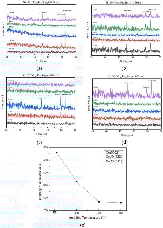
Figure 1.
XRD patterns of Co60Fe20Sm20 films: (a) RT, (b) after annealing at 100 °C, (c) after annealing at 200 °C, (d) after annealing at 300 °C. (e) XRD diffracted peak intensity of all oxides.
The calibrated thickness associated with the sputtering time is exhibited in Figure 2, aiming for accurate thickness calibration. The linear trend observed in the graph suggests that increasing sputtering durations yield thicker films.
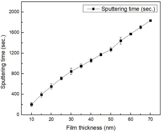
Figure 2.
The calibrated thickness with respect to sputtering time.
3.2. Contact Angle and Surface Energy
The evaluation of contact angles under as-deposited and annealing conditions using a contact angle measurement tool is presented in Figure 3a–d. The procedure involved depositing droplets of DI water and glycerol onto the Co60Fe20Sm20 thin film surface, followed by measuring the resulting contact angles. Figure 3a displays a reduction in the contact angle trend at room temperature (RT) as the thickness increases, observed with both testing liquids. Figure 3b depicts an increasing contact angle trend at an annealing temperature of 100 °C within the thickness range of 10 nm to 30 nm, followed by a decrease within the range of 30 nm to 50 nm, with both testing liquids. Figure 3c,d demonstrate a decreasing contact angle trend with DI water as the thickness increases during annealing at 200 °C and 300 °C. In contrast, the approximate contact angle trend with glycerin increases as the thickness is augmented during annealing at 200 °C and 300 °C. The results clearly indicate that the contact angle values of the as-deposited films exceed those of the annealed films, owing to increased thickness and higher annealing temperatures. This can be attributed to the oxidation effect, resulting in significant surface roughness and an increased contact angle [33]. This behavior mirrors what has been observed in C60 and ZnO studies [34,35]. In the as-grown samples, the contact angle of glycerol decreased with increasing thickness. Conversely, for samples annealed at 300 °C, the opposite trend was observed. As depicted in Figure 1d, oxide peaks were exclusively detected at a thickness of 50 nm when annealed at 300 °C, indicating that oxides can lead to pronounced surface roughness and an elevated contact angle. The analysis of experimental outcomes consistently revealed larger contact angles with deionized water compared to glycerol. Moreover, the contact angles recorded for both types of liquids consistently ranged from 67.7° to 83.3°, remaining below 90°. This suggests the hydrophilic nature of Co60Fe20Sm20 thin films. This experiment affirms that Co60Fe20Sm20 thin films exhibit a favorable interaction with water-based liquids, reflecting a hydrophilic characteristic. Furthermore, this study examines the interplay among contact angle, film thickness, and annealing temperature. The contact angle, a measure of wettability, can be influenced by film thickness and is a key parameter for surface characterization. Moreover, annealing temperature affects the crystallinity, structure, and overall stability of thin films, subsequently influencing contact angle and film thickness [36]. Surface roughness is also a significant factor affecting these contact angles. This study illustrates that as the annealing temperature is increased, surface roughness decreases, leading to a corresponding reduction in contact angle observed during AFM measurements [37,38,39].
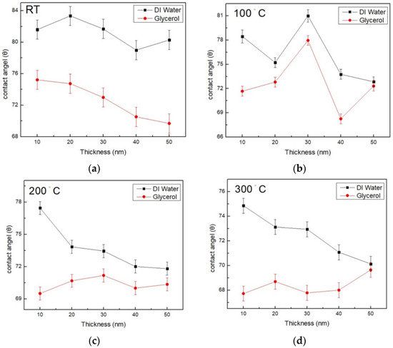
Figure 3.
Contact angle of CoFeSm films: (a) RT, (b) after annealing at 100 °C, (c) after annealing at 200 °C, (d) after annealing at 300 °C.
The surface energy of Co60Fe20Sm20 thin films increases proportionally with both film thickness and annealing temperature, as depicted in Figure 4. The surface energy of Co60Fe20Sm20 films was computed based on contact angle measurements and Young’s equation [22,23,24].
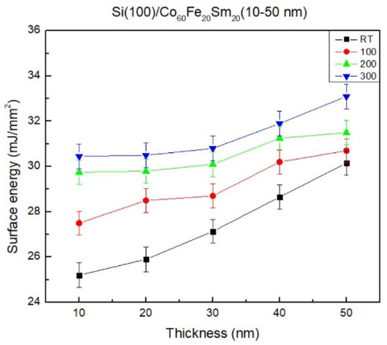
Figure 4.
Surface energy of CoFeSm films.
Young’s equation is
σsg = σsl + σlg cosθ
Specifically, in this context, σsg represents the surface free energy of the solid, σsl stands for the interfacial tension between the liquid and solid, σlg denotes the surface tension of the liquid, and θ is utilized to symbolize the contact angle.
Additionally, post-annealing, there was a noticeable enhancement in the surface energy. Based on these observations, it is now possible to engage in a discussion regarding the annealing temperature of 300 °C. Co60Fe20Sm20 thin films with a 50 nm thickness showcased comparatively elevated the highest surface energy. The decrease in the contact angle observed suggests a rising trend in surface energy, signifying improved adhesion of the thin film. A smaller contact angle corresponds to a higher surface energy [40]. The surface energy of a material is observed to increase with both film thickness and annealing temperature. As the film thickness increases, the surface area also increases, leading to enhanced surface energy. Similarly, elevating the annealing temperature influences the crystalline structure and atomic arrangement of the material, resulting in higher surface energy [41]. When contemplating the potential roles of the Co60Fe20Sm20 film, notably as a seed or buffer layer in double-layer and multi-layer systems, it becomes vital to consider both surface energy and adhesion. The heightened surface energy facilitates effective liquid absorption, leading to a reduction in the contact angle. This phenomenon arises from the stronger attraction between liquid molecules and solid atoms, surpassing the intermolecular forces within the liquid. Also, higher surface energy corresponds to lower surface tension in the liquid, resulting in easier wetting and enhanced adhesion [42].
3.3. Electrical Properties
The resistivity data of CoFeSm films are illustrated in Figure 5a. The graphical depiction evidently illustrates a notable decrease in the resistivity of Co60Fe20Sm20 thin films with both increasing film thickness and rising annealing temperature. Noteworthy is the Co60Fe20Sm20 annealed at 300 °C, with a 50 nm thickness, displaying the lowest resistivity recorded at 8.8 × 10⁻⁶ (Ω-cm). Shifting our attention to Figure 5b, the sheet resistance is examined for Co60Fe20Sm20 thin films. The graph illustrates a clear connection between sheet resistance and resistivity. As film thickness and annealing temperature increase, both sheet resistance and resistivity significantly decrease. This can be explained by the fact that thinner films and lower annealing temperatures lead to a higher presence of oxides and grain boundaries. These factors hinder current carrier transport, leading to elevated resistivity and sheet resistance [43,44]. Particularly, the Co60Fe20Sm20 thin film annealed at 300 °C, with a 50 nm thickness, portrays the lowest sheet resistance value at 3.6 × 10⁻⁵ (×104 Ω/sq) [45]. The relationship between resistivity and the mentioned geometrical factors can often be described through fundamental equations, wherein resistivity (ρ) is a function of these geometrical quantities. For instance, the resistivity can be expressed as Formula (2):
where R is the resistance, A is the cross-sectional area, and L is the length. However, the Si(100) substrates are all set to a uniform 1 cm square size, and the separation between the four-point probe measurement probes is unaltered. Consequently, the only variables impacting the results are the film thickness and the temperature utilized in the heat treatment. Moreover, AFM experiments have confirmed that larger roughness tends to escalate in the as-deposited state as well as with lower annealing temperatures and hinder smooth current flow through the film, resulting in a notable increase in the measured value [45,46,47].
ρ = RA/L
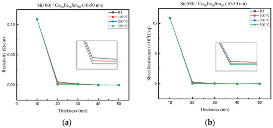
Figure 5.
Electrical properties of CoFeSm films: (a) resistivity, (b) sheet resistance.
3.4. Hardness and Young’s Modulus
The hardness declines with an increase in film thickness, as depicted in Figure 6a. Both Figure 6a,b depict a proportional correlation between Young’s modulus and hardness, showcasing a decline in hardness and Young’s modulus with increasing thickness and annealing temperature. It is probable that this observed trend is due to grain growth, wherein the expansion of grain size diminishes grain boundaries, consequently leading to a reduction in hardness [48]. In addition, the hardness exhibits a consistent decrease with increasing thickness, in accordance with the Hall–Petch effect [49].
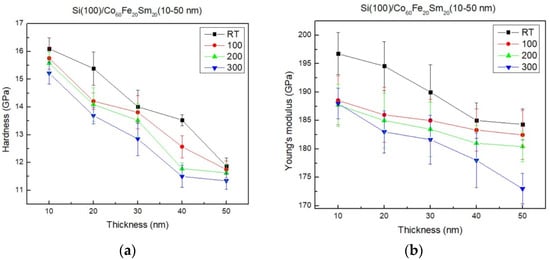
Figure 6.
Hardness and Young’s modulus of CoFeSm films: (a) hardness, (b) Young’s modulus.
3.5. Magnetic Property
The low-frequency alternating current magnetic susceptibility (χac) results for the films at four various conditions are presented in Figure 7a–d. The plots demonstrate an increasing trend in χac values for the Co60Fe20Sm20 films. Moreover, the χac values decrease as the frequency rises. Additionally, it is noticeable that an increase in both film thickness and annealing temperature corresponds to a higher maximum χac value, which is shown in Figure 7e. Interestingly, the highest maximum χac value is achieved at 200 °C, suggesting that this phenomenon is likely linked to the impact of annealing temperature, resulting in a weakening of magnetic properties. Comparatively, the χac values following annealing at 300 °C are diminished compared to those at 200 °C, likely because of an escalated thermal disturbance effect [50]. The maximum χac value escalates with an increase in thickness owing to the thickness effect [51].
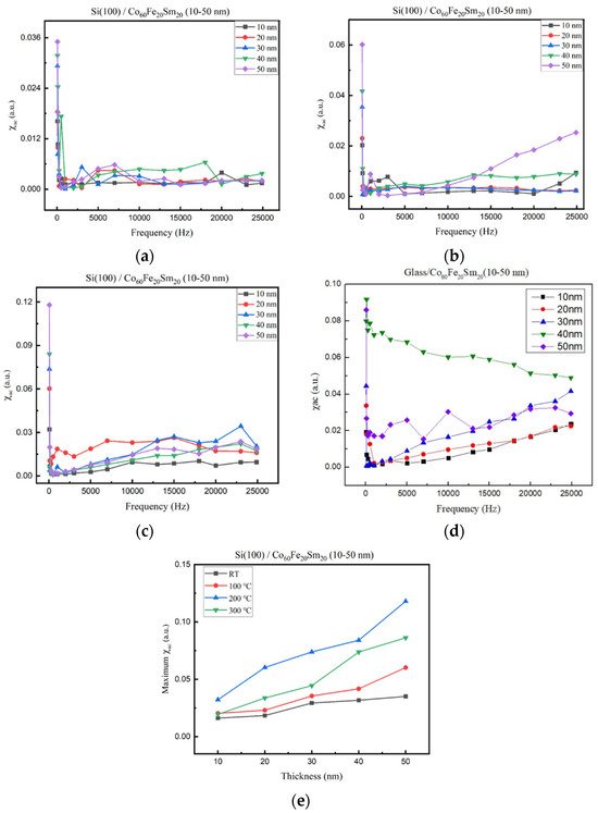
Figure 7.
χac of CoFeSm films under different annealing conditions, including (a) RT, (b) annealing at 100 °C, (c) annealing at 200 °C, (d) annealing at 300 °C, and (e) maximum χac value.
3.6. Surface Characterization of Magnetic Domains in the Thin Film
Upon analyzing the magnetic domain images depicted in Figure 8a–d, a noticeable difference in brightness contrast can be observed. Specifically, in Figure 8d, a noticeable decrease in the brightness contrast of the magnetic domains is evident, signifying a diminishment in the magnetic anisotropy of the film. The observed correlation indicates that the most prominent aspect of the image is the distribution of magnetic domains. The scanning dimensions of the samples cover an area of 20 µm × 20 µm. The magnetic domain morphology of Co60Fe20Sm20 films presents a refined stripe-like pattern. This decline is conjectured to be associated with the emergence of an antiferromagnetic layer on the film’s surface, which is consistent with the magnetic result and indicates the maximum χac of 300 °C is smaller than those at 200 °C [52].
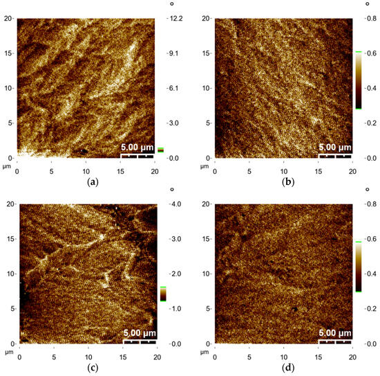
Figure 8.
Magnetic domains of CoFeSm films with a thickness of 50 nm under different annealing conditions, including (a) RT, (b) annealing at 100 °C, (c) annealing at 200 °C, and (d) annealing at 300 °C.
3.7. Characterization of Surface Roughness
The surface roughness and 3D surface topography are displayed in Figure 9a–d. The 3D graphs offer insight into the surface roughness, indicating a subtle improvement in smoothness. Average roughness (Ra) was assessed within a flat region, registering at 4.99 nm at RT and subsequently reducing to 4.22 nm as the heat treatment temperature rose to 300 °C. The observations indicate that utilizing lower sputtering power levels could induce the development of surface protrusions, contributing to uneven grain sizes and an increase in surface roughness [53]. Research in the field suggests that annealing the thin film can lead to a more homogenous surface. It is noted that prior to annealing, incomplete grain ordering is associated with surface irregularities and smaller grain sizes [54]. In summary, the surface roughness of CoFeSm films at different annealing temperatures plays a significant role in shaping their magnetic, electrical, and adhesive properties. Smoother surface roughness reduces the pinning effect on domain walls, making the shift and enhancement of χac value. Furthermore, a smoother surface results in a lower contact angle and higher surface energy. Conversely, rougher surfaces exhibit higher carrier conductivity, leading to a reduction in electrical resistance.
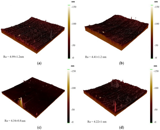
Figure 9.
Surface roughness and 3D surface topography of the 50 nm thick CoFeSm film under various annealing conditions: (a) RT, (b) annealing at 100 °C, (c) annealing at 200 °C, and (d) annealing at 300 °C.
The comparison with other designated materials can be seen in Table 1, including Cobalt Iron Ytterbium (CoFeYb) and Cobalt Iron Yttrium (CoFeY), deposited on Si(100) substrates [55,56]. The information presented in Table 1 highlights that the maximum χac in the current research is lower than observed in Co60Fe20Yb20 and Co60Fe20Y20 materials. Furthermore, the hardness of CoFeSm films is superior to that of CoFeYb films.

Table 1.
Prominent features of Co60Fe20Yb20, Co60Fe20Y20, and Co60Fe20Sm20 films.
4. Conclusions
Analysis by X-ray diffraction (XRD) displays distinct oxide characteristic peaks, including Co (0002), Co2O3 (422), and Co2O3 (511), in the Co60Fe20Sm20 thin films subjected to varying annealing temperatures. It is evident that the contact angle values of the as-deposited films surpass those of the annealed films, primarily due to increased thickness and higher annealing temperatures. This can be attributed to the oxidation effect, leading to significant surface roughness and an augmented contact angle. The increase in both film thickness and annealing temperature directly correlates with an increase in surface energy. Furthermore, the enhancement of film thickness and annealing temperature results in a considerable reduction in sheet resistance and resistivity, facilitated by smoother surface roughness that allows for easier current carrier transport. Both Young’s modulus and hardness display a decreasing trend with increasing thickness and annealing temperature. This is notably observed in the consistent decrease in hardness with increasing thickness, in line with the Hall–Petch effect. Moreover, an increase in the measured frequency corresponds to a clear tendency for the χac value to decrease. There is a noticeable upward trend in the maximum χac as thickness and annealing temperature increase, primarily due to the thickness effect. The maximum χac value is recorded at 200 °C and 50 nm. Notably, after annealing at 300 °C, the χac values experience a notable decrease compared to those at 200 °C, likely because of the heightened thermal disturbance effect. To recapitulate, the magnetic, electric, and adhesive traits of CoFeSm films undergo considerable changes due to surface roughness at different annealing temperatures. A smoother surface with decreased roughness lessens the effects on domain wall pinning, making their movement easier and, consequently, enhancing the χac value. Smoother surface roughness enables a more effortless transport of current carriers. Additionally, surface roughness is correlated with a decline in the contact angle and an augmentation in surface energy. This study points out that the best combination of factors involves annealing at 300 °C with a film thickness of 50 nm, leading to superior adhesion, χac value, and reduced electrical resistance.
Author Contributions
Conceptualization, W.-J.L., Y.-H.C., Y.-T.C. and S.-H.L.; Methodology, Y.-T.C., Y.-H.C., P.-X.L. and Y.-J.H.; Validation, Formal analysis, Y.-T.C., P.-X.L. and Y.-J.H.; Investigation, Y.-T.C. and W.-J.L.; Resources, C.-C.C.; Writing—original draft preparation, Y.-T.C.; Writing—review and editing, Y.-T.C. and W.-J.L.; Supervision, Y.-T.C. and Y.-H.C.; Project administration, Y.-T.C. and S.-H.L.; Funding acquisition, Y.-H.C. and C.-C.C. All authors have read and agreed to the published version of the manuscript.
Funding
This work was supported by the National Science Council, under Grant No. MOST 110-2221-E-992-054-MY3, MOST108-2221-E-224-015-MY3, MOST105-2112-M-224-001, and National Yunlin University of Science and Technology, under Grant No. 111T01 and 113T01.
Institutional Review Board Statement
Not applicable.
Informed Consent Statement
Not applicable.
Data Availability Statement
Not applicable.
Conflicts of Interest
The authors declare that there are no conflict of interest regarding the publication of this paper. The funders had no role in the design of the study; in the collection, analyses, or interpretation of data; in the writing of the manuscript, or in the decision to publish the results.
References
- Xu, Z.; Qin, L. Effects of sputtering parameters and annealing temperatures on magnetic properties of CoFeB films. J. Magn. Magn. Mater. 2021, 538, 168302. [Google Scholar] [CrossRef]
- Skomski, R.; Coey, J. Magnetic anisotropy—How much is enough for a permanent magnet? Scr. Mater. 2016, 112, 3–8. [Google Scholar] [CrossRef]
- Cui, J.; Kramer, M.; Zhou, L.; Liu, F.; Gabay, A.; Hadjipanayis, G.; Balasubramanian, B.; Sellmyer, D. Current progress and future challenges in rare-earth-free permanent magnets. Acta Mater. 2018, 158, 118–137. [Google Scholar] [CrossRef]
- Rachid, F.; Omari, L.; Yamkane, Z.; Lassri, H.; Derkaoui, S.; Nouri, K.; Bouzidi, W.; Bessais, L. Annealing effect on structural, microstructural and magnetic properties of nanocrystalline Er-Co-B alloys for permanent magnet applications. Mater. Chem. Phys. 2019, 228, 60–65. [Google Scholar] [CrossRef]
- Zhang, W.-Y.; Zhang, X.-D.; Yang, Y.-C.; Shen, B.-G. Effect of Cu substitution on structure and magnetic properties of anisotropic SmCo ribbons. J. Alloys Compd. 2003, 353, 274–277. [Google Scholar] [CrossRef]
- Popov, A.; Golovnia, O.; Protasov, A.; Gaviko, V.; Kolodkin, D.; Gopalan, R. Coercivity kinetics upon step annealing of sintered Sm(Co0.88–Fe Cu0.09Zr0.03)7 magnets. J. Rare Earths 2019, 37, 1059–1065. [Google Scholar] [CrossRef]
- Suresh, K.; Gopalan, R.; Rao, D.; Singh, A.; Bhikshamaiah, G.; Muraleedharan, K.; Chandrasekaran, V. Microstructure and coercivity variation in melt-spun Sm–Co–Fe–Zr ribbons. Intermetallics 2010, 18, 2244–2249. [Google Scholar] [CrossRef]
- Coïsson, M.; Celegato, F.; Tiberto, P.; Vinai, F. Magnetic properties of field annealed FeCo thin films. J. Magn. Magn. Mater. 2008, 320, e739–e742. [Google Scholar] [CrossRef]
- Gopalan, R.; Ping, D.H.; Hono, K.; Huang, M.Q.; Smith, B.R.; Chen, Z.; Ma, B.M. Microstructure and magnetic properties of melt-spun Sm(Co0.58Fe0.31Cu0.04Zr0.05B0.02)z ribbons. J. Appl. Phys. 2004, 95, 4962–4967. [Google Scholar] [CrossRef]
- Hua, Y.; Lou, L.; Jiang, B.; Kou, J.; Wang, J.; Li, T.; Gao, J.; Zhang, Q.; Li, X. Effect of Co Content on Microstructures and Magnetic Properties of Anisotropic Bulk TbCu7-type Sm-Co Nanocrystalline Magnets. IEEE Trans. Magn. 2019, 56, 2100104. [Google Scholar] [CrossRef]
- Saito, T.; Hamane, D.N. Magnetic properties of SmCo5−xFex (x = 0–4) melt-spun ribbon. J. Alloys Compd. 2014, 585, 423–427. [Google Scholar] [CrossRef]
- Xi, L.; Du, J.; Zhou, J.; Ma, J.; Li, X.; Wang, Z.; Zuo, Y.; Xue, D. Soft magnetic property and magnetization reversal mechanism of Sm doped FeCo thin film for high-frequency application. Thin Solid Film. 2012, 520, 5421–5425. [Google Scholar] [CrossRef]
- Hashim, M.; Boda, N.; Ahmed, A.; Sharma, S.K.; Ravinder, D.; Sumalatha, E.; Ul-Hamid, A.; Ismail, M.M.; Chaman, M.; Shirsath, S.E.; et al. Influence of samarium doping on structural, elastic, magnetic, dielectric, and electrical properties of nanocrystalline cobalt ferrite. Appl. Phys. A 2021, 127, 526. [Google Scholar] [CrossRef]
- Wang, H.W.; Wang, S.; Cao, Y.; Liu, T.; Zhang, Y. Structure and magnetic properties of alnico alloy doped SmCo5–xCux ribbons. J. Magn. Magn. Mater. 2021, 528, 167821. [Google Scholar] [CrossRef]
- Anwar, M.; Kayani, Z.; Hassan, A.; Riaz, S.; Naseem, S. Managing the micro-structure and properties of Sm-ZnO thin films by tuning the contents of Sm. Phys. B Condes. Matter 2023, 662, 414964. [Google Scholar] [CrossRef]
- Gayen, A.; Modak, R.; Srinivasan, A.; Srinivasu, V.V.; Alagarsamy, P. Thickness dependent magneto-static and magneto-dynamic properties of CoFeB thin films. J. Vac. Sci. Technol. A 2019, 37, 031513. [Google Scholar] [CrossRef]
- Grassi, M.; Geilen, M.; Louis, D.; Mohseni, M.; Brächer, T.; Hehn, M.; Stoeffler, D.; Bailleul, M.; Pirro, P.; Henry, Y. Slow-Wave-Based Nanomagnonic Diode. Phys. Rev. Appl. 2020, 14, 024047. [Google Scholar] [CrossRef]
- Meng, H.; Lum, W.; Sbiaa, R.; Lua, S.; Tan, H.K. Annealing effects on CoFeB-MgO magnetic tunnel junctions with perpendicular anisotropy. J. Appl. Phys. 2011, 110, 033904. [Google Scholar] [CrossRef]
- Vértesy, G.; Gasparics, A.; Griffin, J.M.; Mathew, J.; Fitzpatrick, M.E.; Uytdenhouwen, I. Analysis of Surface Roughness Influence in Non-Destructive Magnetic Measurements Applied to Reactor Pressure Vessel Steels. Appl. Sci. 2020, 10, 8938. [Google Scholar] [CrossRef]
- Favieres, C.; Vergara, J.; Madurga, V. Surface Roughness Influence on Néel-, Crosstie, and Bloch-Type Charged Zigzag Magnetic Domain Walls in Nanostructured Fe Films. Materials 2020, 13, 4249. [Google Scholar] [CrossRef]
- Liu, W.J.; Chang, Y.H.; Chiang, C.C.; Chen, Y.T.; Wang, Y.Z.; Wu, C.L.; Lin, S.H.; Ou, S.L. Thickness, annealing, and surface roughness effect on magnetic and significant properties of Co40Fe40B10Dy10 thin films. Materials 2023, 16, 5995. [Google Scholar] [CrossRef] [PubMed]
- Ma, K.; Chung, T.; Good, R.J. Surface energy of thermotropic liquid crystalline polyesters and polyesteramide. J. Polym. Sci. 1998, 36, 2327–2337. [Google Scholar] [CrossRef]
- Owens, D.K.; Wendt, R.C. Estimation of the surface free energy of polymers. J. Appl. Polym. Sci. 1969, 13, 1741–1747. [Google Scholar] [CrossRef]
- Kaelble, D.H.; Uy, K.C. A Reinterpretation of Organic Liquid-Polytetrafluoroethylene Surface Interactions. J. Adhes. 1970, 2, 50–60. [Google Scholar] [CrossRef]
- Novaković, M.; Popović, M.; Rajić, V. Study on the structural and magnetic properties of e-beam evaporated Co thin films annealed in vacuum. J. Alloys Compd. 2023, 937, 168411. [Google Scholar] [CrossRef]
- Li, G.; Du, J.; Wang, H.; Wang, Q.; Ma, Y.; He, J. High magnetic field induced pillar growth and subsequent magnetic properties of the thermal evaporated Co thin films. Mater. Lett. 2014, 133, 53–56. [Google Scholar] [CrossRef]
- Lan, T.T.B.; Chang, C.-W.; Kuo, M.-R.; Sun, A.A.-C. Strengthening the magnetic properties of Pr-Fe-B thin films using biased substrate. Colloids Surfaces A: Physicochem. Eng. Asp. 2022, 646, 128925. [Google Scholar] [CrossRef]
- Gu, S.; Ji, B.; Wang, C.; Qi, Q.; Zhou, H.-S.; Zhang, Y.; Luo, G.-N. Effects of long-term annealing-induced microstructure evolution on mechanical performance and deuterium release behavior of Li4SiO4 pebbles. Nucl. Fusion 2023, 63, 046006. [Google Scholar] [CrossRef]
- Ramos, R.D.; Boratto, M.H.; Li, M.S.; Scalvi, L.V. Emission Properties Related to Distinct Phases of Sol-Gel Dip-Coating Titanium Dioxide, and Carrier Photo-Excitation in Different Energy Ranges. Mater. Res. 2017, 20, 866–873. [Google Scholar] [CrossRef]
- Tsuchiya, T.; Terabe, K.; Ochi, M.; Higuchi, T.; Osada, M.; Ymashita, Y.; Ueda, S.; Aono, M. In situ tuning of magnetization and magnetoresistance in Fe3O4 thin film achieved with all-solid-state redox device. ACS Nano 2016, 10, 1655–1661. [Google Scholar] [CrossRef]
- Xiang, H.; Shi, F.; Rzchowski, M.; Voyles, P.; Chang, Y.A. Epitaxial growth and magnetic properties of Fe3O4 films on TiN buffered Si(001), Si(110), and Si(111) substrates. Appl. Phys. Lett. 2010, 97, 092508. [Google Scholar] [CrossRef]
- Ishibe, T.; Maeda, Y.; Terada, T.; Naruse, N.; Mera, Y.; Kobayashi, E.; Nakamura, Y. Resistive switching memory performance in oxide hetero-nanocrystals with well-controlled interfaces. Sci. Technol. Adv. Mater. 2020, 21, 195–204. [Google Scholar] [CrossRef] [PubMed]
- Nyong, A.; Rohatgi, P. Underwater Superoleophobicity Induced by the Thickness of the Thermally Grown Porous Oxide Layer on C84400 Copper Alloy. Appl. Sci. 2014, 4, 42–54. [Google Scholar] [CrossRef]
- Kitamura, M.; Kuzumoto, Y.; Kamura, M.; Aomori, S.; Na, J.; Arakawa, Y. Low-voltage-operating fullerene C60 thin-film transistors with various surface treatments. Phys. Stat. Sol. 2008, 5, 3181–3183. [Google Scholar] [CrossRef]
- Beaini, S.S.; Kronawitter, C.X.; Carey, V.P.; Mao, S.S. ZnO deposition on metal substrates: Relating fabrication, morphology, and wettability. J. Appl. Phys. 2013, 113, 184905. [Google Scholar] [CrossRef]
- Azizian-Kalandaragh, Y.; Nouhi, S.; Amiri, M. Effect of post-annealing treatment on the wetting, optical and structural properties of Ag/Indium tin oxide thin films prepared by electron beam evaporation technique. Mater. Express 2015, 5, 137–145. [Google Scholar] [CrossRef]
- Vengesa, Y.; Fattah-Alhosseini, A.; Elmkhah, H.; Imantalab, O.; Keshavarz, M.K. Investigation of corrosion and tribological characteristics of annealed CrN/CrAlN coatings deposited by CAE-PVD. Ceram. Int. 2023, 49, 3016–3029. [Google Scholar] [CrossRef]
- Misyura, S.Y.; Andryushchenko, V.A.; Morozov, V.S. The influence of copper substrate temperature on the wettability of graphene coating. Surf. Innov. 2023, 11, 272–284. [Google Scholar] [CrossRef]
- Madadi, F.; Rezaeian, A.; Edris, H.; Zhiani, M. Influence of surface roughness and hydrophobicity of bipolar plates on PEM performance. Surf. Coat. Technol. 2020, 389, 125676. [Google Scholar] [CrossRef]
- Kalin, M.; Polajnar, M. The wetting of steel, DLC coatings, ceramics and polymers with oils and water: The importance and correlations of surface energy, surface tension, contact angle and spreading. Appl. Surf. Sci. 2014, 293, 97–108. [Google Scholar] [CrossRef]
- Kunwar, S.; Pandey, P.; Sui, M.; Zhang, Q.; Li, M.-Y.; Lee, J. Effect of Systematic Control of Pd Thickness and Annealing Temperature on the Fabrication and Evolution of Palladium Nanostructures on Si (111) via the Solid State Dewetting. Nanoscale Res. Lett. 2017, 12, 364. [Google Scholar] [CrossRef] [PubMed]
- Sharma, P.; Ponte, F.; Lima, M.; Figueiredo, N.; Ferreira, J.; Carvalho, S. Plasma etching of polycarbonate surfaces for improved adhesion of Cr coatings. Appl. Surf. Sci. 2023, 637, 157903. [Google Scholar] [CrossRef]
- Kalpana, H.M.; Prasad, V.S.; Nayak, M.M. Influence of annealing and thickness on the electrical properties of invar36 thin film for strain gauge applications. Int. J. Thin Film. Sci. Technol. 2013, 2, 155–161. [Google Scholar] [CrossRef] [PubMed]
- Lin, Q.; Zhang, A.; Zhao, A.; Yang, P. Influence of annealing temperature on optical properties of sandwiched ZnO/Metal/ZnO transparent conductive thin films. Micromachines 2022, 13, 296. [Google Scholar] [CrossRef]
- Butt, M.Z.; Ali, D.; Tanveer, M.; Naseem, S. Surface roughness and electrical resistivity of high-purity zinc irradiated with nanosecond visible laser pulses. Appl. Sur. Sci. 2014, 305, 466–473. [Google Scholar] [CrossRef]
- Marom, H.; Eizenberg, M. The effect of surface roughness on the resistivity increase in nanometric dimensions. J. Appl. Phys. 2006, 99, 123705. [Google Scholar] [CrossRef]
- Aihaiti, L.; Tuokedaerhon, K.; Saden, B.; Zhang, M.; Shenm, X.; Mijito, A. Effect of annealing temperature on microstructure and resistivity of TiC thinfilms. Coatings 2021, 11, 457. [Google Scholar] [CrossRef]
- Wen, T.; Gong, J.; Peng, Z.; Jiang, D.; Wang, C.; Fu, Z.; Miao, H. Analysis of continuous stiffness data measured during nanoindentation of titanium films on glass substrate. Mater. Chem. Phys. 2011, 125, 500–504. [Google Scholar] [CrossRef]
- Zhang, S.; Sun, D.; Fu, Y.; Du, H. Recent advances of superhard nanocomposite coatings: A review. Surf. Coat. Technol. 2003, 167, 113–119. [Google Scholar] [CrossRef]
- Sousa, W.; Guerra, Y.; Peña-Garcia, R.; Padrón-Hernández, E. Saturation magnetization as a function of temperature in Zn doped YIG nanoparticles. Phys. E Low-Dimens. Syst. Nanostruct. 2021, 138, 115054. [Google Scholar] [CrossRef]
- Wang, K.; Xu, Z.; Huang, Y.; Qiu, Y.; Dong, S. Magnetic, thermal, electrical properties and crystallization kinetics of Co60Fe20B20 alloy films. Sci. China Mater. 2016, 59, 639–647. [Google Scholar] [CrossRef]
- Pandey, M.K.; Kar, A.K. Effect of annealing temperature on the magnetic domain structure and surface mechanical properties of Ni-C composite thin films: Magnetic and lateral force microscopy, and force-distance spectroscopy. Mater. Lett. 2021, 301, 130295. [Google Scholar] [CrossRef]
- Liu, L.; Li, W.; Sun, H.; Wang, G. Effects of Ti Target Purity and Microstructure on Deposition Rate, Microstructure and Properties of Ti Films. Materials 2022, 15, 2661. [Google Scholar] [CrossRef] [PubMed]
- Yang, Y.; Maeng, B.; Jung, D.; Lee, J.; Kim, Y.; Kwon, J.; An, H.; Jung, D. Annealing effects on SnO2 thin film for H2 Gas Sensing. Nanomaterials 2022, 12, 3227. [Google Scholar] [CrossRef] [PubMed]
- Liu, W.J.; Chang, Y.H.; Chen, Y.T.; Chiu, P.C.; Guo, J.C.; Lin, S.H.; Chi, P.W. Effects of annealing and thickness of Co60Fe20Yb20 nanofilms on their structure, magnetic properties, electrical efficiency, and nanomechanical characteristics. Materials 2022, 15, 5184. [Google Scholar] [CrossRef] [PubMed]
- Liu, W.J.; Chang, Y.H.; Chen, Y.T.; Tsai, D.Y.; Lu, P.X.; Lin, S.H.; Wu, T.H.; Chi, P.W. Effect of yttrium addition on structure and magnetic characteristics of Co60Fe20Y20 films. Materials 2021, 14, 6001. [Google Scholar] [CrossRef] [PubMed]
Disclaimer/Publisher’s Note: The statements, opinions and data contained in all publications are solely those of the individual author(s) and contributor(s) and not of MDPI and/or the editor(s). MDPI and/or the editor(s) disclaim responsibility for any injury to people or property resulting from any ideas, methods, instructions or products referred to in the content. |
© 2023 by the authors. Licensee MDPI, Basel, Switzerland. This article is an open access article distributed under the terms and conditions of the Creative Commons Attribution (CC BY) license (https://creativecommons.org/licenses/by/4.0/).