Review

X-ray Detectors Based on Halide Perovskite Materials

1
School of Optics and Photonics, Beijing Institute of Technology, Beijing 100081, China
2
Beijing Key Laboratory for Precision Optoelectronic Measurement Instrument and Technology, Beijing 100081, China
3
Yangtze Delta Region Academy of Beijing Institute of Technology, Jiaxing 314019, China
*
Authors to whom correspondence should be addressed.
Coatings 2023, 13(1), 211; https://doi.org/10.3390/coatings13010211
Submission received: 11 December 2022 / Revised: 9 January 2023 / Accepted: 12 January 2023 / Published: 16 January 2023
(This article belongs to the Special Issue Application of Advanced Quantum Dots Films in Optoelectronics)

Abstract

:
Halide perovskite has remarkable optoelectronic properties, such as high atomic number, large carrier mobility-lifetime product, high X-ray attenuation coefficient, and simple and low-cost synthesis process, and has gradually developed into the next-generation X-ray detection materials. Halide perovskite-based X-ray detectors can improve the sensitivity and reduce the detectable X-ray dose, which is applied in imaging, nondestructive industrial inspection, security screening, and scientific research. In this article, we introduce the fabrication methods of halide perovskite film and the classification and progress of halide perovskite-based X-ray detectors. Finally, the existing challenges are discussed, and the possible directions for future applications are explored. We hope this review can stimulate the further improvement of perovskite-based X-ray detectors.

1. Introduction

X-ray detectors are commonly used in medical imaging, nondestructive industrial inspection, safety screening, and scientific research [1,2,3]. High sensitivity and high detection efficiency are believed to be critical figures of merit for X-ray detectors because weak X-ray signals can be detected, which greatly reduces the risk of medical examination [4,5,6]. The performance is closely related to the features of X-ray detection semiconductor materials including atomic number, charge carrier mobility, and carrier lifetime [7,8,9]. Various semiconductor materials have been utilized in X-ray detectors, such as silicon (Si), amorphous selenium (α-Se), germanium (Ge), and cadmium zinc telluride (CdZnTe). In addition, diamond is considered the elective material for X-ray detection and has a wide range of applications in the radiotherapy field mainly due to its “tissue equivalence” characteristic [10,11,12,13]. However, traditional materials such as α-Se, Ge, and CdZnTe suffer from many issues, including relatively small atomic numbers, the low attenuation coefficient of X-rays, and complex and costly fabrication processes [14,15,16]. Thus, it is necessary to explore new materials to replace the traditional materials for X-ray detectors.
Halide perovskites with a formula of ABX3 (where A = CH3NH3+ (MA+), HC(NH2)2+ (FA+) and Cs+; B = Pb2+ or Sn2+; X = halides) are emerging candidates in X-ray detection. They have very high X-ray attenuation coefficients, a large carrier mobility-lifetime product (μτ product), a high atomic number, and a simple and low-cost synthesis process [17,18]. The summarization of the parameters of the materials for X-ray detectors is shown in Table 1. X-ray detectors employing organic–inorganic hybrid perovskite materials such as MAPbI3 and MAPbBr3 and all-inorganic perovskite materials such as CsPbBr3 have been reported. According to the structural dimensionalities of halide perovskites, various types of materials with different characteristics of three-dimensional, low-dimensional, and three-dimensional/low-dimensional hybrid perovskite appear successively. Moreover, different techniques are used for the fabrication of high-quality halide perovskite films, which is the premise for achieving useful X-ray detectors. However, reviews that comprehensively summarize the fabrication methods of halide perovskite films and the features of halide perovskite-based X-ray detectors with different structural dimensionalities and different organic and inorganic components are relatively rare.
This review introduces in detail the fabrication methods of halide perovskite films and then summarizes the progress of research and development of halide perovskite-based X-ray detectors. Figure 1 shows the main fabrication methods and types of detectors introduced in this review. Finally, according to the progress of halide perovskite-based X-ray detectors, the existing problems are discussed, and the possible directions for future applications are explored.

2. Halide Perovskite Film Fabrication Methods

The quality of the film is the key factor to determine the performance of perovskite-based X-ray detectors. Fabrication methods are classified as a spin-coating process, dissolution and recrystallization method, spray deposition process, aerosol–liquid–solid method, solution growth method, scraper method, inkjet printing method, and laser direct writing and melt and crystallization. In the following, we describe these methods, introduce representative works, and analyze their features.

2.1. Spin-Coating Process

Spin coating is an early and widely used technology in perovskite film processing due to its simple and easy operation process. The process is mainly divided into two steps: dropping the solution on the cleaned substrate and accelerating the rotating plate to a required velocity. A uniform film is formed on the substrate because of the solution diffusion and solvent evaporation at high speed. The thickness of the film depends on the concentration, density, and spin velocity of the solution. In 2015, Yakunin et al. fabricated an X-ray detector based on methylammonium lead iodide perovskite (CH3NH3PbI3) perovskite materials through the spin-coating process [27]. Uniform perovskite films deposited onto patterned electrode structures are accomplished through spin-coating technology (Figure 2a). Although the achievable film quality is high, the spin-coating process suffers from the difficulty of scaling up to large-area substrates. In addition, the rotational speed, solution concentration, etc., of different solutions need to be reexplored to obtain the desired thickness.

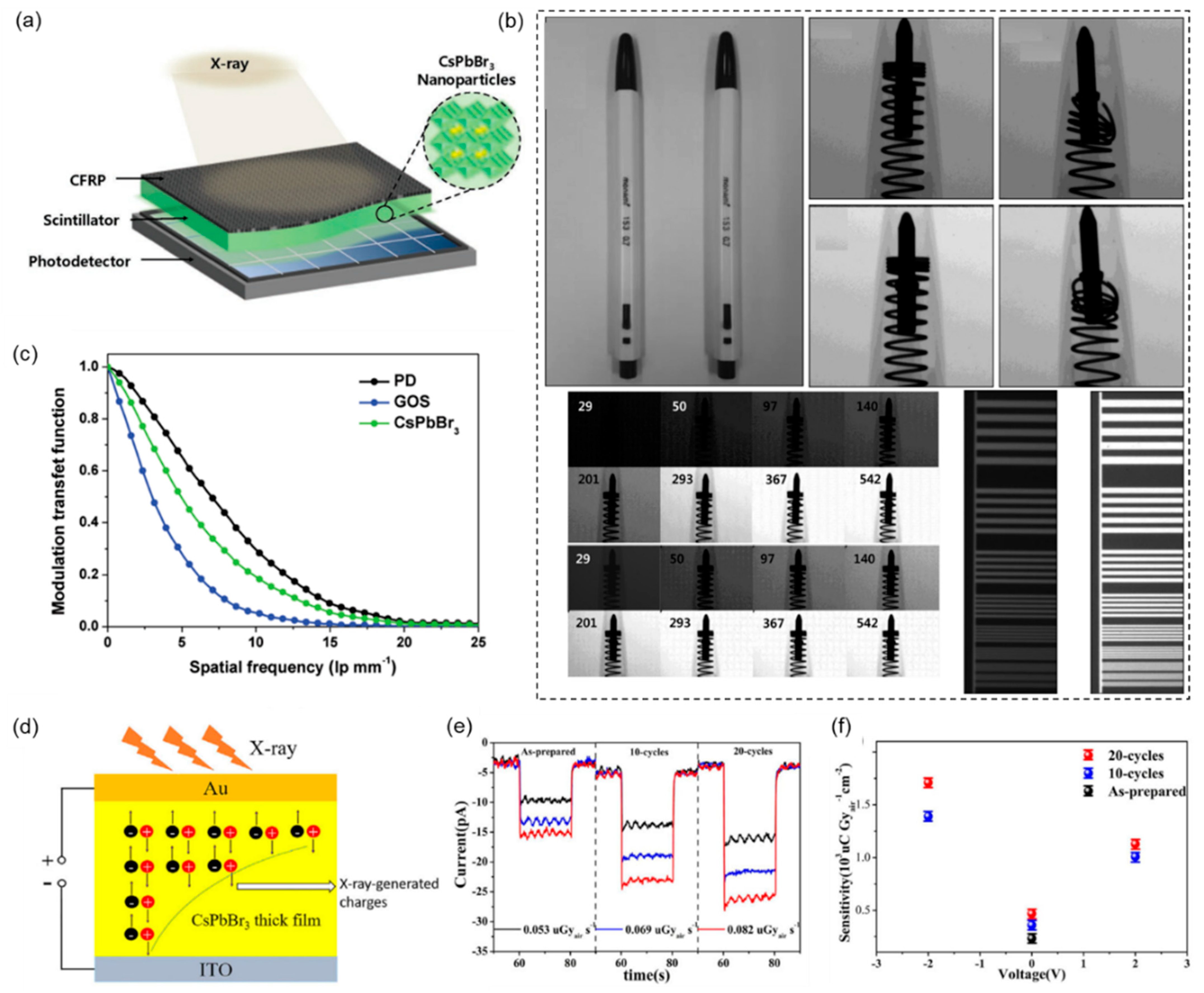
2.2. Dissolution and Recrystallization Method

The dissolution and recrystallization process is an efficient method for the preparation of high-quality perovskite films. During many dissolution and recrystallization processes, the sharp portion of the surface particles of the film is dissolved in the original perovskite solution. This dissolved material recrystallizes at the right temperature, filling the holes in the surface. After this repeated process, smooth and dense thick perovskite films can be obtained. In 2019, Zongyan Gou et al. ameliorated the film of the CsPbBr3 microcrystalline after many dissolutions and recrystallizations, laying a good foundation for obtaining a high-performance X-ray detector (Figure 2b) [26]. The scanning electron microscope (SEM) images of the CsPbBr3 films after repairing at different times are shown in Figure 2c. The surface of the original membrane is rough and full of holes. With the increase in dissolution and recrystallization times, the surface of the CsPbBr3 film becomes microporous and smooth. This indicates that the rigid part of the CsPbBr3 crystal on the surface of the film gradually dissolves into the original perovskite solution, leading to the filling of the holes.

2.3. Spray Deposition Process

The spray deposition process is one of the low-cost and large-scale production manufacturing methods for perovskite films (Figure 2d). The perovskite can be easily modified into ink to form a uniform perovskite film by a spray deposition process. In 2020, Koth Amratisha et al. developed the continuous spray deposition technique to realize the layer-by-layer stacking structure of different perovskite materials (Figure 2e) [28]. The perovskite film stability can be well maintained in a humid environment owing to the spray deposition preparation method. Sequential spray deposition technology opens up a new way for perovskite film stacking design and mass production under economical ambient conditions.

2.4. Aerosol–Liquid–Solid Method

The aerosol–liquid–solid method is a streamlined circulation from aerosol to liquid to solid, which can be used for the preparation of perovskite film. A suite of technological parameters including temperature, aerosol supply rate, and composition can be precisely controlled for aerosol–liquid–solid method technology. Due to surface tension and viscosity limitations, it is tough to deposit very thick wet films on the substrate through traditional solution methods such as spin-coating methods; however, the aerosol–liquid–solid method could achieve dense, high crystallinity, low defect density thick perovskite film around 1 mm (Figure 2f). In 2021, Wei Qian et al. demonstrated aerosol–liquid–solid methods to enable the continued growth of homogeneous perovskite films [29]. The thickness and grain size of the film increase gradually with the increase in growth time, as shown in Figure 2g.

2.5. Solution Growth Method

The solution growth method has the advantages of a low-cost, large-scale, and fast growth rate, which is suitable for the growth of perovskite single crystal. In 2016, Haotong Wei et al. successfully fabricated solution-grown MAPbBr3 single crystals with extraordinary optoelectronic properties [30]. In 2020, Xin Wang et al. achieved the solution-processed epitaxial growth of MAPbX3 organic–inorganic hybrid perovskite single crystal with different halide components and no lattice mismatch [31]. Figure 3a shows the SEM images of the cross-section and surface characterization of the solution-processed epitaxial layer, revealing the growth of a single-crystal film from a small island into a flat film.

2.6. Scraper Method

The scraper method is one of the crafts for producing films. In 1952, a scraper method patent was obtained by scraping water-based and non-water-based slurry onto moving plasterboard. Recently, the scraper method has been applied in the fabrication of perovskite films. When a constant relative motion is established between the blade and the substrate, the perovskite slurry is spread over the substrate to form a thin perovskite film. The scraper can run at a speed of several meters/per min. This operation mode is suitable for coating wet perovskite films with a thickness of tens of microns to hundreds of microns [32,33]. In 2017, Yong Churl Kim et al. used a scraper method to fabricate an 830 μm-thick polycrystalline MAPbI3 layer [34]. In 2022, Mengling Xia et al. applied a combination of the scraper method and a soft pressure-assisted cryogenic solution treatment to make high-quality films for thin-film transistor (TFT) integration (Figure 3b) [35]. The method realizes the compatibility between the perovskite material and the TFT substrate and helps to achieve compact perovskite films with a smooth surface and passivated grain boundaries.

2.7. Inkjet Printing Method

Inkjet printing technology represents a highly established method for thin-film manufacturing with applications in electronics, optics, bioengineering, and other fields [36]. This technology has the advantages of low manufacturing costs, a simple and flexible process, and no mask plate and lithography, which can be widely used in perovskite solution printing [37,38]. Figure 3c illustrates the basic components of an inkjet printer including an ink chamber, conducting nozzle, substrate, and translational stage [39]. When a voltage is applied between the substrate and the nozzle, a curved liquid surface is formed at the nozzle under the action of the induced electric field force [40]. As the voltage gradually increases, small droplets are formed and ejected onto the substrate (Figure 3d) [41]. The movement of the nozzle and the mode of the applied voltage can control the pattern printed on the substrate [39,40,41]. In 2019, Jingying Liu et al. homogeneously prepared perovskite films on different nature substrates by the inexpensive inkjet printing method (Figure 3e) [42]. The cheap and simple inkjet printing method enables the large-scale manufacturing of multi-channel arrays of perovskite-based X-ray detectors.

2.8. Laser Direct Writing

Laser direct writing is a common method for preparing nanostructured graphics. Laser direct writing technology is widely used in all-inorganic halide perovskite colloidal quantum dots. In 2017, Chen Jun et al. proposed a rapid preparation method of perovskite colloidal quantum-dot film based on laser direct writing. It is simple, fast, and does not require a mask [43]. It includes three steps: spin-coating perovskite colloidal quantum dots, laser writing, and solvent washing (Figure 3f). Moreover, a large-scale (100 mm × 100 mm) perovskite colloidal quantum-dot patterning is demonstrated by the laser direct writing technology.
Figure 3. Solution growth, scraper, inkjet printing, and laser direct writing methods. (a) SEM photos of epitaxial layer cross-section and solution treatment at different growth times. Reprinted with permission from Ref. [31]. 2020, American Chemical Society. (b) Scraper method and a soft pressure-assisted cryogenic solution treatment. Reprinted with permission from Ref. [35]. 2022, Wiley. (c) Schematic of inkjet printer. Reprinted with permission from Ref. [39]. 2012, IOP Publishing. (d) Schematic illustration of inkjet printing system. Reprinted with permission from Ref. [41]. 2015, Royal Society of Chemistry. (e) Schematic diagram of a perovskite-based device manufactured by inkjet printing. Reprinted with permission from Ref. [42]. 2019, Wiley. (f) Schematic diagram of the modeling process and mechanism of perovskite colloidal quantum dots. Reprinted with permission from Ref. [43]. 2017, Wiley.
Coatings 13 00211 g003

2.9. Melt and Crystallization

Perovskite has various forms such as nanocrystals, nanowires, and polycrystalline films, among which perovskite single crystal is the more stable form. Melt and crystallization are the preferred methods to obtain perovskite crystals. In this way, high-quality perovskite single crystals can be grown from the melt, which can meet the requirements of large diameters and cause less pollution during the synthesis process. In 2022, Andrii Kanak et al. studied the melting and crystallization process of all-organic perovskite CsPbBr3, obtained massive single crystals from the melt, discussed the phase transition mechanism of the whole process, and proposed the two-stage melting mechanism of CsPbBr3 perovskite. The effect of heating and cooling conditions on the crystallization process of large particle CsPbBr3 was studied. This study is helpful to further understanding the crystal structure and crystallization mechanism of perovskite. It is important for understanding the growth and high-quality preparation of perovskite crystals and massive perovskite materials [44].

3. Halide Perovskite-Based X-ray Detector

Recently, there have been many high-impact review papers on introducing perovskite-based X-ray detectors. Zhizai Li et al. reviewed the current research progress on halide perovskite-based X-ray detectors [45]. Joydip Ghosh et al. summarized recent efforts on lead-free double perovskite-based X-ray detectors [46]. Haodi Wu et al. advised scalable fabrication of metal halide perovskite-based X-ray detectors [47].
Halide perovskite as an emerging X-ray detection material has a long carrier lifetime, large atomic numbers, and high X-ray attenuation coefficient [23,48]. An X-ray detector based on halide perovskite material possesses high detection sensitivity, which is crucial for detecting weak X-ray dose rates and greatly reducing the risk of medical examination [45]. Moreover, the synthesis process of halide perovskite is simple and low-cost as previously mentioned, which could form large-area flat panel detector arrays at low cost. Halide perovskite-based X-ray detector with high sensitivity and low cost has great application prospects in security, defense, medical imaging, industrial materials inspection, and nuclear power plants [49,50,51].
There are various structural dimensionalities of perovskites by controlling appropriate organic and inorganic components, such as 3D and low-dimensional (2D, 1D, 0D) perovskites. In recent years, various halide perovskite-based X-ray detectors have been developed by utilizing different dimensional perovskites. The three main types of halide perovskite-based X-ray detectors are described in detail below, including 3D, low, and 3D/low-dimensional mixed perovskite-based X-ray detectors. The summarization of the performance of X-ray detectors based on halide perovskite materials is shown in Table 2.

3.1. 3D Perovskites-Based X-ray Detectors

3D perovskites have a universal formula of ABX3 (where A is a monovalent organic or inorganic cation, B is a divalent cation, and X is halide anion) and are composed of continuous corner-sharing metal halide [BX6]4− octahedra [52]. According to the organic and inorganic components, 3D perovskites-based X-ray detectors are mainly divided into two representative types: organic–inorganic hybrid perovskites and all-inorganic perovskites-based X-ray detectors.

3.1.1. Organic–Inorganic Hybrid Perovskites-Based X-ray Detectors

Organic–inorganic hybrid perovskites have been shown to have good optoelectronic properties for X-ray detection, including a large appropriate band gap (1.6–3.0 eV) and a large μτ product on the order of ~10−2 cm2 V−1 [53]. In 2017, Wei Wei et al. fabricated a MAPbBr3 single-crystal X-ray detector and integrated it onto the Si substrates. This allows the electrical signal to be read directly from the Si (Figure 4a) [53]. The brominated (3-amino-propyl) triethoxy-silane (NH3Br) end molecular layer is used to mechanically and electrically connect the MAPbBr3 single crystals to the Si. No lattice matching with the Si substrate is required. The sensitivity of the MAPbBr3 single-crystal X-ray detector is 2.1 × 10⁴ µC Gyair−1 cm−2 under 8 keV X-ray radiation, which is more than 1000 times that of the commercially available amorphous α-Se detector. As shown in Figure 4b, it is possible to achieve X-ray imaging at a low X-ray (8 keV) dose rate of <0.1 μGyair s−1.
Although halide perovskite X-ray detectors have had great success, the high concentration of Pb in perovskite poses a serious threat to human and biological systems due to its high water solubility. “Green” bi-element with the same electronic structure as the Pb attracts wide attention. In 2017, Weicheng Pan et al. demonstrated sensitive X-ray detectors using solution-processed double perovskite Cs2AgBiBr6 single crystals [54]. The Cs2AgBiBr6 single crystals use one Ag+ and one Bi3+ to substitute two toxic Pb2+ in CsPbBr3, which are very friendly to humans and biological systems (Figure 4c,d). In addition, after heat annealing and surface treatment, the Ag+/Bi3+ disordering is eliminated and the crystal resistivity is enhanced. The Cs2AgBiBr6 single crystals exhibit a higher resistivity (109–1011 Ω cm) than MAPbX3 (X = Cl, Br, I; 107–108 Ω cm). As a result, the Cs2AgBiBr6 single-crystal X-ray detectors possess a low minimum dose rate of 59.7 nGyair s−1 under 5 V and a high sensitivity of 8 µC Gyair−1 cm−2 (1 V bias) to 30 keV X-ray photons and 105 µC Gyair−1 cm−2 at 50 V (Figure 4e).

3.1.2. All-Inorganic Perovskites-Based X-ray Detectors

Although the hybrid organic–inorganic perovskite-based X-ray detectors have realized outstanding performance, the stability of hybrid organic–inorganic perovskite is poor. This has an impact on their actual use, hindering their use in practical applications. The environmental conditions of their storage, fabrication, and device operation are very strict due to the extreme sensitivity to both oxygen and moisture. In addition, they are also unstable to light and heat due to the influence of organic groups. All-inorganic cesium halide lead perovskite (CsPbX3) without organic components is considered to be the next generation of X-ray detector materials due to its superior stability to hybrid perovskite.
In 2018, Jin Hyuck Heo et al. prepared a CsPbX3 perovskite nanocrystalline X-ray detector that is easy to commercialize and cost-effective (Figure 5a) [55]. The acquired X-ray detectors exhibit high stability over X-ray irradiation of 40 Gyair s−1. Moreover, the X-ray imaging possesses an excellent spatial resolution of 9.8 lp mm−1 at modulation transfer function (MTF) = 0.2 and 12.5–8.9 lp mm−1 for a linear line chart, which is higher than commercial terbium-doped gadolinium oxysulfide (GOS) detectors of spatial resolution = 6.2 lp mm−1 at MTF = 0.2 and 6.3 lp mm−1 for a linear line chart (Figure 5b,c).
In 2019, Zongyan Gou et al. fabricated X-ray detectors based on the CsPbX3 microcrystal thick film. The multi-dissolution and recrystallization method is used to further improve the photoelectric performance of the detector (Figure 5d) [26]. The sensitivity of CsPbX3-based X-ray detectors is 470 µC Gyair−1 cm−2 at zero bias under a remarkably low dose rate (0.053 µGyair s−1), which is over 20 times higher than that of α-Se X-ray detectors working at a much higher field of 10 V µm−1 (Figure 5e,f).

3.2. Low-Dimensional Perovskites-Based X-ray Detectors

Although 3D perovskites-based X-ray detectors achieve high sensitivity, the phase transformation and instability of 3D perovskites limit their development. To address these issues of 3D perovskites, low-dimensional perovskites have been developed and high-performance low-dimensional perovskites-based X-ray detectors have been realized.

3.2.1. Organic–Inorganic Hybrid Perovskites-Based X-ray Detectors

(NH4)3Bi2I9 belongs to organic–inorganic hybrid perovskite-related materials A3M2X9 (A = Cs, Rb, NH4; M = Bi, Sb; X = Br, I). The (NH4)3Bi2I9 has a 2D layered structure where the BiI6 octahedra corners share each other and are stacked in a close-packed fashion in the (001) plane (Figure 6a) [56]. In 2019, Renzhong Zhuang et al. verified the 2D (NH4)3Bi2I9 without toxic elements is a suitable material to obtain a high-performance X-ray detector [56]. Layered (NH4)3Bi2I9 grows easily in low-temperature solutions and can be cut along cleavage planes (Figure 6b,c). Two types of (NH4)3Bi2I9-based X-ray detectors with parallel and perpendicular device structures were proposed, as shown in Figure 6d. The devices were exposed to a source with X-ray photon energy up to 50 keV and with a peak intensity of 22 keV. The sensitivity of the parallel direction device is high at 8.2 × 10³ µC Gyair−1 cm−2, which is higher than that of the perpendicular one (803 µC Gyair−1 cm−2). Moreover, the perpendicular direction device possesses a lower detection limit of 55 nGyair s−1 compared to the parallel one of 210 nGyair s−1 (Figure 6e).

3.2.2. All-Inorganic Perovskites-Based X-ray Detectors

0D perovskite quantum dots are ideal candidates for X-ray detectors and large-area flat or flexible panels with great application potential. CsPbBr3 materials as a typical all inorganic perovskite possess superior stability and excellent optoelectronic properties. In 2019, Jingying Liu et al. synthesized 0D high-quality colloidal CsPbBr3 perovskite quantum dots via the hot injection method at room temperature and demonstrated a flexible, printable CsPbBr3-based X-ray detector (Figure 7a–c) [42]. Perovskite quantum-dot films are printed evenly on a variety of substrates using an inexpensive inkjet printing method to demonstrate large-scale manufacturing of X-ray detector arrays. The device was exposed to a synchrotron soft X-ray beamline with photon energies ranging from 0.1 to 2.5 keV. The detector has a sensitivity of 1450 μGyairs−1 cm−2 at 0.0172 mGyairs−1 X-ray dose rate and a bias voltage of only 0.1 V, which is 70 times more sensitive than the α-Se device. Moreover, the CsPbBr3 quantum-dot-based X-ray detectors possess outstanding flexibility and durability (Figure 7d–f).

3.3. Three-Dimensional/Low-Dimensional Hybrid Perovskites-Based X-ray Detectors

3D perovskites such as MAPbI3, MAPbBr3, and CsPbBr3 are conducive to achieving high sensitivity due to their long carrier lifetime. However, baseline drifting problems arising from ion migration in the 3D perovskite material prevent accurate signal recording, hindering practical applications. Low-dimensional perovskites such as 2D BDAPbI4 (BDA = NH3C4H8NH3) and (NH4)3Bi2I9 can effectively solve the baseline drifting problems. However, the sensitivity of low-dimensional perovskite is limited by its poor carrier transport performance. Thus, the combination of the 3D and low-dimensional perovskites could be an effective choice beyond the performance of X-ray detection with individual dimension perovskites.
In 2021, Xiuwen Xu et al. developed a double-layer perovskite film with a properly aligned energy level, where 2D (PEA)2MA3Pb4I13 (PEA = 2-phenylethylammonium, MA = methylammonium) is cascaded with vertically crystallized 3D MAPbI3 (Figure 8a–d) [57]. Combining the fast carrier transport of the 3D layer and mitigated ion migration of the 2D layer, X-ray detectors provide high sensitivity and very stable baselines. Moreover, the 2D layer increases the film resistivity and enlarges the energy barrier for the hole injection without compromising carrier extraction (Figure 8e–g). As a result, the obtained double-layer perovskite detector exhibits a high sensitivity (1.95 × 10⁴ µC Gyair−1 cm−2) and a low detection limit (480 nGyair s−1) (Figure 8h). The double-layer perovskite detector exhibits excellent stability and a highly repeatable X-ray response when the X-ray is periodically on/off (Figure 8i). X-ray images of the printed circuit boards obtained with a double-layer perovskite detector with an active area of 3 mm × 3 mm are shown in Figure 8j.
Table 2. The summarization of the performance of halide perovskite-based X-ray detectors.
TypeMaterialFabrication MethodFilm Thickness
(μm)
Sensor Area
(mm2)
Sensitivity
(µC Gyair−1 cm−2)
Minimum Detectable Dose Rate (µGyairs−1)Ref.
3D perovskites-based X-ray detectorsMAPbBr3Solution-processed molecular bonding method1500.04421,000<0.1 (−1 V)[53]
Solution growth method2000-800.5 (−0.1 V)[30]
Cs2AgBiBr6Solution-processed method11803.14105 (50 V)0.0597 (5 V)[54]
CsPbBr3Laser direct writing-10,000--[43]
Dissolution and recrystallization method18504700.053 (2 V)[26]
Melt and crystallization----[44]
CH3NH3PbI3Spin-coating process10–100---[27]
CsPbI2BrAerosol–liquid–solid methodOne micrometer- hundreds of micrometers10,000148,0000.28 (0.125 V μm−1)[29]
MAPbI3Scraper method40078,40017,432 (500 V mm−1)0.067 (5 V mm−1)[35]
Low-dimensional perovskites-based X-ray detectors(NH4)3Bi2I9Solution growth method4900 (parallel);
1500 (perpendicular)
6.75 (parallel); 22 (perpendicular)8200 (parallel); 803 (perpendicular)0.21 (parallel 1 V); 0.055 (perpendicular 10 V)[56]
CsPbBr3Inkjet printing method0.60.06145017.2 (0.1 V)[42]
3D/low-dimensional hybrid perovskites-based X-ray detectors2D (PEA)2MA3Pb4I13
/3D MAPbI3
Spray deposition process0.5919,5000.48 (<25 V mm−1)[57]

4. Challenges and Perspectives

A variety of materials have been studied for X-ray detection because X-ray detectors have a wide range of applications including medical imaging, nondestructive industrial inspection, and safety screening. Diamond is considered the elective material for X-ray detection, mainly due to its “tissue equivalence” [10,11,12,13]. Recently, halide perovskites are emerging candidates in X-ray detection owing to the high X-ray attenuation coefficients, large μτ product, high atomic number, and the simple and low-cost synthesis process. Although halide perovskite-based X-ray detectors have made many remarkable signs of progress in the past few years, there are still some important problems that need further consideration to meet application requirements. The existing challenges are discussed, and the possible directions for future applications are explored in the following.
Firstly, compared with traditional materials such as Si, α-Se, and Ge, the stability of perovskite materials is still relatively poor, which seriously restricts their practical application. Therefore, more attention should be paid to improving the stability of perovskite materials in future research.
Secondly, the thickness of perovskite films with hundreds of micrometers is the prerequisite for complete X-ray attenuation. However, the fabrication of a thick perovskite film with good uniformity is still a challenge. Moreover, the cost of preparation of perovskite-based X-ray detectors should be further reduced. Hence, developing new preparation methods or optimizing the original methods is the future development trend.
Thirdly, the sensitivity and minimum detectable X-ray dose rate of perovskite-based X-ray detectors are not good enough for practical use. It is necessary to develop high-performance perovskite-based X-ray detectors with high sensitivity and low detection limits.
Finally, the development of large-area flexible next-generation X-ray detection and imaging technology based on perovskite is the future research direction.

Author Contributions

Conceptualization, X.T.; investigation, Y.T. and G.M.; writing—original draft preparation, Y.T. and G.M.; writing—review and editing, Y.T., G.M. and X.T.; supervision, X.T.; project administration, X.T.; funding acquisition, X.T., G.M. and M.C. All authors have read and agreed to the published version of the manuscript.

Funding

This work was funded by the National Key R&D Program of China (2021YFA0717600), the National Natural Science Foundation of China (NSFC No. 62035004 and NSFC No. 62105022) and the China Postdoctoral Science Foundation (2022M710396). X.T. is sponsored by the Young Elite Scientists Sponsorship Program by CAST (No. YESS20200163).

Institutional Review Board Statement

Not applicable.

Informed Consent Statement

Not applicable.

Data Availability Statement

Not applicable.

Conflicts of Interest

The authors declare no conflict of interest.

References

  1. Kasap, S.; Kabir, M.Z.; Rowlands, J. Recent advances in X-ray photoconductors for direct conversion X-ray image detectors. Curr. Appl. Phys. 2006, 6, 288–292. [Google Scholar] [CrossRef]
  2. Long, M.; Zhang, T.; Xu, W.; Zeng, X.; Xie, F.; Li, Q.; Chen, Z.; Zhou, F.; Wong, K.S.; Yan, K. Large-grain formamidinium PbI3–xBrx for high-performance perovskite solar cells via intermediate halide exchange. Adv. Energy Mater. 2017, 7, 1601882. [Google Scholar] [CrossRef]
  3. Su, Y.; Ma, W.; Yang, Y.M. Perovskite semiconductors for direct X-ray detection and imaging. J. Semicond. 2020, 41, 51204. [Google Scholar] [CrossRef]
  4. Mescher, H.; Schackmar, F.; Eggers, H.; Abzieher, T.; Zuber, M.; Hamann, E.; Baumbach, T.; Richards, B.S.; Hernandez-Sosa, G.; Paetzold, U.W. Flexible inkjet-printed triple cation perovskite X-ray detectors. ACS Appl. Mater. Interfaces 2020, 12, 15774–15784. [Google Scholar] [CrossRef] [PubMed]
  5. Pan, W.; Yang, B.; Niu, G.; Xue, K.H.; Du, X.; Yin, L.; Zhang, M.; Wu, H.; Miao, X.S.; Tang, J. Hot-Pressed CsPbBr3 Quasi-Monocrystalline Film for Sensitive Direct X-ray Detection. Adv. Mater. 2019, 31, 1904405. [Google Scholar] [CrossRef]
  6. Basiricò, L.; Ciavatti, A.; Fraboni, B. Solution-Grown Organic and Perovskite X-Ray Detectors: A New Paradigm for the Direct Detection of Ionizing Radiation. Adv. Mater. Technol. 2021, 6, 2000475. [Google Scholar] [CrossRef]
  7. Sun, C.; Shen, X.; Zhang, Y.; Wang, Y.; Chen, X.; Ji, C.; Shen, H.; Shi, H.; Wang, Y.; William, W.Y. Highly luminescent, stable, transparent and flexible perovskite quantum dot gels towards light-emitting diodes. Nanotechnology 2017, 28, 365601. [Google Scholar] [CrossRef]
  8. Wang, W.; Ma, Y.; Qi, L. High-performance photodetectors based on organometal halide perovskite nanonets. Adv. Funct. Mater. 2017, 27, 1603653. [Google Scholar] [CrossRef]
  9. Hu, H.; Niu, G.; Zheng, Z.; Xu, L.; Liu, L.; Tang, J. Perovskite semiconductors for ionizing radiation detection. EcoMat 2022, 4, e12258. [Google Scholar] [CrossRef]
  10. Pettinato, S.; Girolami, M.; Olivieri, R.; Stravato, A.; Caruso, C.; Salvatori, S. A diamond-based dose-per-pulse x-ray detector for radiation therapy. Materials 2021, 14, 5203. [Google Scholar] [CrossRef]
  11. Pettinato, S.; Girolami, M.; Olivieri, R.; Stravato, A.; Caruso, C.; Salvatori, S. Time-resolved dosimetry of pulsed photon beams for radiotherapy based on diamond detector. IEEE Sens. J. 2022, 22, 12348–12356. [Google Scholar] [CrossRef]
  12. Talamonti, C.; Kanxheri, K.; Pallotta, S.; Servoli, L. Diamond Detectors for Radiotherapy X-Ray Small Beam Dosimetry. Front. Phys. 2021, 9, 632299. [Google Scholar] [CrossRef]
  13. Marinelli, M.; Felici, G.; Galante, F.; Gasparini, A.; Giuliano, L.; Heinrich, S.; Pacitti, M.; Prestopino, G.; Vanreusel, V.; Verellen, D. Design, realization, and characterization of a novel diamond detector prototype for FLASH radiotherapy dosimetry. Med. Phys. 2022, 49, 1902–1910. [Google Scholar] [CrossRef] [PubMed]
  14. Grancini, G.; Roldán-Carmona, C.; Zimmermann, I.; Mosconi, E.; Lee, X.; Martineau, D.; Narbey, S.; Oswald, F.; De Angelis, F.; Graetzel, M. One-Year stable perovskite solar cells by 2D/3D interface engineering. Nat. Commun. 2017, 8, 1–8. [Google Scholar] [CrossRef] [Green Version]
  15. Bakr, Z.H.; Wali, Q.; Fakharuddin, A.; Schmidt-Mende, L.; Brown, T.M.; Jose, R. Advances in hole transport materials engineering for stable and efficient perovskite solar cells. Nano Energy 2017, 34, 271–305. [Google Scholar] [CrossRef] [Green Version]
  16. Rao, H.-S.; Chen, B.-X.; Wang, X.-D.; Kuang, D.-B.; Su, C.-Y. A micron-scale laminar MAPbBr 3 single crystal for an efficient and stable perovskite solar cell. Chem. Commun. 2017, 53, 5163–5166. [Google Scholar] [CrossRef]
  17. Haruta, Y.; Kawakami, M.; Nakano, Y.; Kundu, S.; Wada, S.; Ikenoue, T.; Miyake, M.; Hirato, T.; Saidaminov, M.I. Scalable Fabrication of Metal Halide Perovskites for Direct X-ray Flat-Panel Detectors: A Perspective. Chem. Mater. 2022, 34, 5323–5333. [Google Scholar] [CrossRef]
  18. Büchele, P.; Richter, M.; Tedde, S.F.; Matt, G.J.; Ankah, G.N.; Fischer, R.; Biele, M.; Metzger, W.; Lilliu, S.; Bikondoa, O. X-ray imaging with scintillator-sensitized hybrid organic photodetectors. Nat. Photonics 2015, 9, 843–848. [Google Scholar] [CrossRef]
  19. Luo, Z.; G Moch, J.; S Johnson, S.; Chon Chen, C. A review on X-ray detection using nanomaterials. Curr. Nanosci. 2017, 13, 364–372. [Google Scholar] [CrossRef]
  20. Owens, A. Semiconductor materials and radiation detection. J. Synchrotron Radiat. 2006, 13, 143–150. [Google Scholar] [CrossRef]
  21. Bellazzini, R.; Spandre, G.; Brez, A.; Minuti, M.; Pinchera, M.; Mozzo, P. Chromatic X-ray imaging with a fine pitch CdTe sensor coupled to a large area photon counting pixel ASIC. J. Instrum. 2013, 8, C02028. [Google Scholar] [CrossRef] [Green Version]
  22. Guo, J.; Xu, Y.; Yang, W.; Zhang, B.; Dong, J.; Jie, W.; Kanatzidis, M.G. Morphology of X-ray detector Cs 2 TeI 6 perovskite thick films grown by electrospray method. J. Mater. Chem. C 2019, 7, 8712–8719. [Google Scholar] [CrossRef]
  23. Wei, H.; Huang, J. Halide lead perovskites for ionizing radiation detection. Nat. Commun. 2019, 10, 1–12. [Google Scholar] [CrossRef] [PubMed] [Green Version]
  24. Kabir, M.Z.; Kasap, S. Photoconductors for x-ray image detectors. In Springer Handbook of Electronic and Photonic Materials; Springer: Berlin/Heidelberg, Germany, 2017; p. 1. [Google Scholar]
  25. Matt, G.J.; Levchuk, I.; Knüttel, J.; Dallmann, J.; Osvet, A.; Sytnyk, M.; Tang, X.; Elia, J.; Hock, R.; Heiss, W. Sensitive Direct Converting X-Ray Detectors Utilizing Crystalline CsPbBr3 Perovskite Films Fabricated via Scalable Melt Processing. Adv. Mater. Interfaces 2020, 7, 1901575. [Google Scholar] [CrossRef] [Green Version]
  26. Gou, Z.; Huanglong, S.; Ke, W.; Sun, H.; Tian, H.; Gao, X.; Zhu, X.; Yang, D.; Wangyang, P. Self-Powered X-Ray Detector Based on All-Inorganic Perovskite Thick Film with High Sensitivity Under Low Dose Rate. Phys. Status Solidi (RRL)–Rapid Res. Lett. 2019, 13, 1900094. [Google Scholar] [CrossRef]
  27. Yakunin, S.; Sytnyk, M.; Kriegner, D.; Shrestha, S.; Richter, M.; Matt, G.J.; Azimi, H.; Brabec, C.J.; Stangl, J.; Kovalenko, M.V. Detection of X-ray photons by solution-processed lead halide perovskites. Nat. Photonics 2015, 9, 444–449. [Google Scholar] [CrossRef]
  28. Amratisha, K.; Ponchai, J.; Kaewurai, P.; Pansa-Ngat, P.; Pinsuwan, K.; Kumnorkaew, P.; Ruankham, P.; Kanjanaboos, P. Layer-by-layer spray coating of a stacked perovskite absorber for perovskite solar cells with better performance and stability under a humid environment. Opt. Mater. Express 2020, 10, 1497–1508. [Google Scholar] [CrossRef]
  29. Qian, W.; Xu, X.; Wang, J.; Xu, Y.; Chen, J.; Ge, Y.; Chen, J.; Xiao, S.; Yang, S. An aerosol-liquid-solid process for the general synthesis of halide perovskite thick films for direct-conversion X-ray detectors. Matter 2021, 4, 942–954. [Google Scholar] [CrossRef]
  30. Wei, H.; Fang, Y.; Mulligan, P.; Chuirazzi, W.; Fang, H.-H.; Wang, C.; Ecker, B.R.; Gao, Y.; Loi, M.A.; Cao, L. Sensitive X-ray detectors made of methylammonium lead tribromide perovskite single crystals. Nat. Photonics 2016, 10, 333–339. [Google Scholar] [CrossRef]
  31. Wang, X.; Li, Y.; Xu, Y.; Pan, Y.; Zhu, C.; Zhu, D.; Wu, Y.; Li, G.; Zhang, Q.; Li, Q. Solution-processed halide perovskite single crystals with intrinsic compositional gradients for X-ray detection. Chem. Mater. 2020, 32, 4973–4983. [Google Scholar] [CrossRef]
  32. Uhland, S.A.; Holman, R.K.; Morissette, S.; Cima, M.J.; Sachs, E.M. Strength of green ceramics with low binder content. J. Am. Ceram. Soc. 2001, 84, 2809–2818. [Google Scholar] [CrossRef]
  33. Baklouti, S.; Bouaziz, J.; Chartier, T.; Baumard, J.-F. Binder burnout and evolution of the mechanical strength of dry-pressed ceramics containing poly (vinyl alcohol). J. Eur. Ceram. Soc. 2001, 21, 1087–1092. [Google Scholar] [CrossRef]
  34. Kim, Y.C.; Kim, K.H.; Son, D.-Y.; Jeong, D.-N.; Seo, J.-Y.; Choi, Y.S.; Han, I.T.; Lee, S.Y.; Park, N.-G. Printable organometallic perovskite enables large-area, low-dose X-ray imaging. Nature 2017, 550, 87–91. [Google Scholar] [CrossRef] [PubMed]
  35. Xia, M.; Song, Z.; Wu, H.; Du, X.; He, X.; Pang, J.; Luo, H.; Jin, L.; Li, G.; Niu, G. Compact and Large-Area Perovskite Films Achieved via Soft-Pressing and Multi-Functional Polymerizable Binder for Flat-Panel X-Ray Imager. Adv. Funct. Mater. 2022, 32, 2110729. [Google Scholar] [CrossRef]
  36. Onses, M.S.; Sutanto, E.; Ferreira, P.M.; Alleyne, A.G.; Rogers, J.A. Mechanisms, capabilities, and applications of high-resolution electrohydrodynamic jet printing. Small 2015, 11, 4237–4266. [Google Scholar] [CrossRef]
  37. Chen, D.; Liang, J.; Pei, Q. Flexible and stretchable electrodes for next generation polymer electronics: A review. Sci. China Chem. 2016, 59, 659–671. [Google Scholar] [CrossRef]
  38. Park, H.-G.; Byun, S.-U.; Jeong, H.-C.; Lee, J.-W.; Seo, D.-S. Photoreactive spacer prepared using electrohydrodynamic printing for application in a liquid crystal device. ECS Solid State Lett. 2013, 2, R52. [Google Scholar] [CrossRef]
  39. Sutanto, E.; Shigeta, K.; Kim, Y.; Graf, P.; Hoelzle, D.; Barton, K.; Alleyne, A.; Ferreira, P.; Rogers, J.A. A multimaterial electrohydrodynamic jet (E-jet) printing system. J. Micromech. Microeng. 2012, 22, 045008. [Google Scholar] [CrossRef] [Green Version]
  40. de Gans, B.J.; Schubert, U.S. Inkjet printing of polymer micro-arrays and libraries: Instrumentation, requirements, and perspectives. Macromol. Rapid Commun. 2003, 24, 659–666. [Google Scholar] [CrossRef]
  41. Kim, K.; Kim, G.; Lee, B.R.; Ji, S.; Kim, S.-Y.; An, B.W.; Song, M.H.; Park, J.-U. High-resolution electrohydrodynamic jet printing of small-molecule organic light-emitting diodes. Nanoscale 2015, 7, 13410–13415. [Google Scholar] [CrossRef]
  42. Liu, J.; Shabbir, B.; Wang, C.; Wan, T.; Ou, Q.; Yu, P.; Tadich, A.; Jiao, X.; Chu, D.; Qi, D. Flexible, printable soft-X-ray detectors based on all-inorganic perovskite quantum dots. Adv. Mater. 2019, 31, 1901644. [Google Scholar] [CrossRef] [PubMed]
  43. Chen, J.; Wu, Y.; Li, X.; Cao, F.; Gu, Y.; Liu, K.; Liu, X.; Dong, Y.; Ji, J.; Zeng, H. Simple and fast patterning process by laser direct writing for perovskite quantum dots. Adv. Mater. Technol. 2017, 2, 1700132. [Google Scholar] [CrossRef]
  44. Kanak, A.; Kopach, O.; Kanak, L.; Levchuk, I.; Isaiev, M.; Brabec, C.J.; Fochuk, P.; Khalavka, Y. Melting and Crystallization Features of CsPbBr3 Perovskite. Cryst. Growth Des. 2022, 22, 4115–4121. [Google Scholar] [CrossRef]
  45. Li, Z.; Zhou, F.; Yao, H.; Ci, Z.; Yang, Z.; Jin, Z. Halide perovskites for high-performance X-ray detector. Mater. Today 2021, 48, 155–175. [Google Scholar] [CrossRef]
  46. Ghosh, J.; Sellin, P.J.; Giri, P.K. Recent advances in lead-free double perovskites for x-ray and photodetection. Nanotechnology 2022, 33, 312001. [Google Scholar] [CrossRef]
  47. Wu, H.; Ge, Y.; Niu, G.; Tang, J. Metal halide perovskites for X-ray detection and imaging. Matter 2021, 4, 144–163. [Google Scholar] [CrossRef]
  48. Sytnyk, M.; Deumel, S.; Tedde, S.F.; Matt, G.J.; Heiss, W. A perspective on the bright future of metal halide perovskites for X-ray detection. Appl. Phys. Lett. 2019, 115, 190501. [Google Scholar] [CrossRef]
  49. Kasap, S.; Frey, J.B.; Belev, G.; Tousignant, O.; Mani, H.; Greenspan, J.; Laperriere, L.; Bubon, O.; Reznik, A.; DeCrescenzo, G. Amorphous and polycrystalline photoconductors for direct conversion flat panel X-ray image sensors. Sensors 2011, 11, 5112–5157. [Google Scholar] [CrossRef] [Green Version]
  50. Yaffe, M.; Rowlands, J. X-ray detectors for digital radiography. Phys. Med. Biol. 1997, 42, 1. [Google Scholar] [CrossRef]
  51. Tegze, M.; Faigel, G. X-ray holography with atomic resolution. Nature 1996, 380, 49–51. [Google Scholar] [CrossRef]
  52. Sun, S.; Lu, M.; Gao, X.; Shi, Z.; Bai, X.; Yu, W.W.; Zhang, Y. 0D perovskites: Unique properties, synthesis, and their applications. Adv. Sci. 2021, 8, 2102689. [Google Scholar] [CrossRef] [PubMed]
  53. Wei, W.; Zhang, Y.; Xu, Q.; Wei, H.; Fang, Y.; Wang, Q.; Deng, Y.; Li, T.; Gruverman, A.; Cao, L. Monolithic integration of hybrid perovskite single crystals with heterogenous substrate for highly sensitive X-ray imaging. Nat. Photonics 2017, 11, 315–321. [Google Scholar] [CrossRef]
  54. Pan, W.; Wu, H.; Luo, J.; Deng, Z.; Ge, C.; Chen, C.; Jiang, X.; Yin, W.-J.; Niu, G.; Zhu, L. Cs2AgBiBr6 single-crystal X-ray detectors with a low detection limit. Nat. Photonics 2017, 11, 726–732. [Google Scholar] [CrossRef]
  55. Heo, J.H.; Shin, D.H.; Park, J.K.; Kim, D.H.; Lee, S.J.; Im, S.H. High-performance next-generation perovskite nanocrystal scintillator for nondestructive X-ray imaging. Adv. Mater. 2018, 30, 1801743. [Google Scholar] [CrossRef] [PubMed]
  56. Zhuang, R.; Wang, X.; Ma, W.; Wu, Y.; Chen, X.; Tang, L.; Zhu, H.; Liu, J.; Wu, L.; Zhou, W. Highly sensitive X-ray detector made of layered perovskite-like (NH4) 3Bi2I9 single crystal with anisotropic response. Nat. Photonics 2019, 13, 602–608. [Google Scholar] [CrossRef]
  57. Xu, X.; Qian, W.; Wang, J.; Yang, J.; Chen, J.; Xiao, S.; Ge, Y.; Yang, S. Sequential Growth of 2D/3D Double-Layer Perovskite Films with Superior X-Ray Detection Performance. Adv. Sci. 2021, 8, 2102730. [Google Scholar] [CrossRef]
Figure 1. Progress in X-ray detectors based on halide perovskite materials.
Coatings 13 00211 g001
Figure 2. Spin-coating, dissolution and recrystallization, spray deposition, and aerosol–liquid–solid methods. (a) The cross-sectional optical microscopy of perovskite films and the scale bar is 100 µm. Reprinted with permission from Ref. [27]. 2015, Springer Nature. (b) CsPbBr3 thick film preparation and repair process diagram. Reprinted with permission from Ref. [26]. 2019, Wiley. (c) SEM images of (i) the original CsPbBr3 thick film, and the treated thick films with (ii) 5, (iii) 10, and (iv) 20 times dissolution and recrystallization. Reprinted with permission from Ref. [26]. 2019, Wiley. (d) Spraying device for depositing double-layer perovskite film. Reprinted with permission from Ref. [28]. 2020, Optica. (e) SEM cross-sections of different layers of perovskite solar cells. Reprinted with permission from Ref. [28]. 2020, Optica. (f) Comparison of traditional solution-based approach to film production (left) and the aerosol–liquid–solid method (right). This highlights the latter’s unique ability to manufacture high-quality thick perovskite films. Reprinted with permission from Ref. [29]. 2021, Cell Press. (g) Cross-section (upper) and top-view SEM images (lower) of perovskite films fabricated by the aerosol–liquid–solid method after 4 (left) and 100 growth cycles (right). Reprinted with permission from Ref. [29]. 2021, Cell Press.
Coatings 13 00211 g002
Figure 4. 3D organic–inorganic hybrid perovskites-based X-ray detectors. (a) Preparation diagram of Si-integrated MAPbBr3 single crystal. Reprinted with permission from Ref. [53]. 2017, Springer Nature. (b) This device was used for the X-ray imaging in stacked glass coverslips; a stainless-steel plate with etched-through lines, a wrapped metal spring, a section of the tail fin, and an “N” copper sign gave a dose rate of 247 nGyair s−1. Reprinted with permission from Ref. [53]. 2017, Springer Nature. (c) X-ray diffraction of Cs2AgBiBr6 single crystal. Illustration: Crystal structure. The small wine ball represents Br, the large khaki ball represents Cs+, and the light green and purple octahedra represent the AgBr6 and BiBr6 octahedra, respectively. Reprinted with permission from Ref. [54]. 2017, Springer Nature. (d) Thermogravimetric analysis of Cs2AgBiBr6. Included is a photograph of a solution-processed Cs2AgBiBr6 single crystal. Reprinted with permission from Ref. [54]. 2017, Springer Nature. (e) The signal-to-noise ratio of the device is calculated from the standard deviation of the X-ray photocurrent. The red dashed line represents a signal-to-noise ratio of 3, and thus the detection limit is 59.7 nGyair s−1 at 5 V bias; it is represented by purple stars surrounded by red dotted circles. Reprinted with permission from Ref. [54]. 2017, Springer Nature.
Coatings 13 00211 g004
Figure 5. 3D all-inorganic perovskites-based X-ray detectors. (a) Schematic diagram of the structure of a CsPbBr3 perovskite nanocrystalline scintillation X-ray detector. Reprinted with permission from Ref. [55]. 2018, Wiley. (b) Photographic and X-ray images for nondestructive inspection. Images of a normal ballpoint pen (left) and defective ballpoint pen (right) with identical appearance, ballpoint pen X-ray images from conventional GOS scintillator X-ray detectors, ballpoint pen X-ray images from CsPbBr3 scintillator X-ray detectors, ballpoint pen X-ray images from GOS and CsPbBr3 scintillator X-ray detectors with X-ray dose rates, line plots taken by GOS and CsPbBr3 scintillation X-ray detectors. Reprinted with permission from Ref. [55]. 2018, Wiley. (c) MTF of the original silicon-based detector, CsPbBr3, and conventional GOS scintillation X-ray detector. Reprinted with permission from Ref. [55]. 2018, Wiley. (d) Thick film radiation detector structure. The charge-producing region lies inside the thick film and is used for X-ray excitation. Reprinted with permission from Ref. [26]. 2019, Wiley. (e) Zero bias light response of raw and treated film at different dose rates. Reprinted with permission from Ref. [26]. 2019, Wiley. (f) The sensitivity of a device under different bias voltages and fixed emissivity (0.053 µGyair s−1). Reprinted with permission from Ref. [26]. 2019, Wiley.
Coatings 13 00211 g005
Figure 6. Low-dimensional organic–inorganic hybrid perovskites-based X-ray detectors. Reprinted with permission from Ref. [56]. 2019, Springer Nature. (a) Crystal structure of (NH4)3Bi2l9 along the c and b axes. (b) Photograph of a bulk (NH4)3Bi2I9 single crystal. (c) Procedure for crystal growth. (d) Illustration of parallel and perpendicular device structures. (e) The signal-to-noise ratio of the device in directions parallel to and perpendicular to the (001) surface. The dashed blue line indicates a signal-to-noise ratio of 3, so the detection limits are 210 nGyair s−1 for parallel devices and 55 nGyair s−1 for vertical devices.
Coatings 13 00211 g006
Figure 7. Low-dimensional all-inorganic perovskites-based X-ray detectors. Reprinted with permission from Ref. [42]. 2019, Wiley. (a) Schematic diagram of a perovskite-based device manufactured by inkjet printing. (b) Photography of an X-ray detector array on a 4-inch wafer. (c) Optical imaging equipment with the printing of quantum-dot film. Scale: 5 µm. Illustration: Low-power image. Scale: 50 µm. (d) Chemical reactions of flexible perovskite-based X-ray detector arrays on polyethylene terephthalate (PET) substrates. (e) Photography of flexible devices under bending. (f) Current and voltage curves of flexible device arrays at different bending angles under X-ray irradiation with 7.33 mGyairs−1 and 0.1 V bias voltages. Inset: Real device showing 120° bending.
Coatings 13 00211 g007
Figure 8. Three-dimensional/low-dimensional hybrid perovskites-based X-ray detectors. Reprinted with permission from Ref. [57]. 2021, Wiley. (a) Schematic diagram illustrating the structure of a double-layer perovskite thin film, where gradient 2D perovskite was prepared from a precursor solution with the nominal component (PEA)2MA3Pb4I13. (bd) SEM image of double-layer perovskite film, shown in (b) is the grain size distribution. (e) Double-layer perovskite X-ray detector equipment configuration: Carbon electrodes were exposed to incident X-ray photons and negatively biased, whereas gradient 2D perovskite was prepared from a precursor solution with the designated component (PEA)2MA3Pb4I13. (f) Control the interfacial level alignment of a device made of a double-layer perovskite film. (g) Band edge position diagram of two-dimensional perovskite and three-dimensional MAPbI3 with respect to fluorine-doped SnO2 (FTO) and carbon. (h) The dose-rate-dependent signal-to-noise ratio of control and double-layer perovskite detectors. (i) Stability test of double-layer perovskite detector under different dose rate X-ray irradiation. (j) A digital photograph of the printed circuit board (size: 5.1 cm × 5.1 cm) and X-ray images of a printed circuit board obtained with a double-layer perovskite detector with an active area of 3 mm × 3 mm.
Coatings 13 00211 g008
Table 1. The summarization of the parameters of the materials for X-ray detectors.
MaterialAtomic
Number
Density
(g cm−3)
Band Gap (eV)μτ Product
(cm2 V−1)
Resistivity
(Ω cm)
Ref.
Si142.331.12>1104[19]
α-Se344.32.1–2.210−7104–105[20]
CdTe48, 526.21.441.5 × 104108–109[21]
Cd0.9Zn0.1Te48, 30, 525.781.5710−21011[21,22]
PbI282, 536.22.3–2.610−51013[20]
HgI280, 536.42.1310−41013[23]
Ge325.331.57>150[24]
CsPbBr356.44.552.2–2.331.3 × 10−28.5 × 10⁹[25]
MAPbI335.64.31.5–1.610−4–10−7-[26]
MAPbBr335, 823.452.2–2.3--[5]
Diamond123.525.25–5.5--[10,11,12,13,20]
Disclaimer/Publisher’s Note: The statements, opinions and data contained in all publications are solely those of the individual author(s) and contributor(s) and not of MDPI and/or the editor(s). MDPI and/or the editor(s) disclaim responsibility for any injury to people or property resulting from any ideas, methods, instructions or products referred to in the content.

