1. Introduction
Aluminum nitride (AlN) belongs to the family of III-Nitride materials with the largest bandgap (6.2 eV) for any semiconductor material that has the native substrate; in addition, it has high thermal, chemical, mechanical stability, and very high Baliga (BFOM) [
1,
2,
3]. Due to these properties and ease to grow on sapphire substrates, AlN is highly desired for its applications in high-power photonic and electronic devices [
3]. For these devices, high-quality AlN films on sapphire substrate with low dislocation density are used as low-cost templates that allow to grow low dislocation density device structures, as high dislocations adversely affect their performance [
4,
5,
6]. The state-of-the-art method to grow low-cost AlN templates is metal-organic chemical vapor deposition (MOCVD) with sapphire as a substrate [
4]. The precursors to grow AlN using MOCVD are trimethyl-aluminum (TMA)/triethyl-aluminum (TEA) as aluminum source and ammonia (NH
3) to be used as nitrogen (N
2) source [
5]. These precursors are precisely delivered on the substrate’s surface in a reaction or growth chamber by hydrogen (H
2) that acts as a carrier/push gas. Thus, the MOCVD process inside the growth chamber would occur in an H
2 environment. An alternative to that approach is to use N
2 as carrier/push gas since N
2 gas is cheaper and safer to use than H
2 gas. The use of N
2 as a carrier gas in AlN growth was first reported on SiC substrates in 2007 [
6]. The first report of AlN growth on sapphire substrates with N
2 as a carrier gas was published in 2012, which reported low-quality samples [
7]. Recently, we have reported that N
2 gas can be used as an alternative to H
2 carrier gas to grow high-quality AlN films with dislocation densities of 10
9/cm
2 for 4 µm thick sample, a cheaper and safer approach [
8,
9]. Thus, a comparative spectroscopic study is warranted to understand the AlN material growth accomplished in these two different gas environments.
This paper reports the spectroscopic comparison of 3 μm thick AlN samples on a sapphire substrate produced by the MOCVD process with N2 and H2 as carrier gases. The grown samples were characterized using spectroscopic techniques to understand the impurity incorporation, stress-strain, dislocations, and surface morphology.
2. Experimental Methods
The AlN samples used for this study were grown using the MOCVD process. A general schematic is shown in
Figure 1 and their details were presented in our recently published papers [
8,
9]. Trimethyl aluminum (TMA) and ammonia (NH
3) were used as aluminum (Al) and nitrogen (N) precursors. The growth process consists of a 2-step process: a low temperature (~950 °C) high V/III ratio (~4000) precursor pulsed rough buffer layer, followed by a low V/III ratio (~1000) high temperature (~1250 °C) continuous growth step. We restricted the thickness of the AlN layers to 3 µm for comparison. In the case of the AlN sample grown with the H
2 carrier gas, an additional low-temperature interlayer was introduced to reduce the crack and achieve the 3 µm thickness (repetition of steps in
Figure 1 after 1.5 µm thickness). Susceptor rotation was introduced for the growth uniformity on the substrate.
The grown AlN films were characterized for their surface morphology, dislocation densities, residual stress, and impurities. The surface morphology of grown AlN was observed with Digital Nanoscope 3100 atomic force microscopy (AFM, Veeco Instruments Inc., Plainview, NY, USA). The Philips X’pert MRD triple-axis diffractometer (Philips, Eindhover, The Netherlands) with Cu-Kα1 X-ray source was used to calculate dislocation densities. A scanning electron microscope Zeiss Supra 25 FE-SEM (Carl Zeiss, Munich, Germany) was used to study the AlN samples’ cross-section along the growth direction. Residual stress in the samples was measured by Raman spectroscopy using Horiba Raman Spectroscope (Horiba, Kyoto, Japan) with a 638 nm red excitation laser with 25% power with 2400 g/mm grating and 100 µm diameter aperture and 50 µm slit size in backscattered mode with a spectral resolution of 0.5 cm
−1. A Kratos AXIS Ultra DLD (Kratos Analytical, Manchester, UK) set up with a monochromatic Al Kα source (1.5 keV) at a 45° incident angle was used for X-ray photoelectron spectroscopy of the samples. Argon ions were used to analyze the samples’ depth with an etch rate of 3 nm/min. XPS Peak 41 software was used to carry out the curve fitting with Gaussian and Lorentzian functions, where Shirley-type background was subtracted [
10,
11]. The Secondary Ion Mass Spectroscopy (SIMS) measurements were performed at the Georgia Tech. Material Characterization Facility using an IONTOF TOF-SIMS 5-300 instrument (IONTOF, Münster, Germany). The Time of Flight (ToF) SIMS machine uses two ion guns: one for sputtering only and another one for analysis purposes. For sputtering, cesium ions were used with an energy of 2 keV for creating a crater and bismuth ions with 25 keV for analyzing the sputtered area along the way. To measure these samples, they were mounted on a sample holder using Cu tape, and the sputtering created a crater area of 300 μm
2; the area of analysis by the bismuth ions was 150 μm
2. Room-temperature cathodoluminescence (CL) measurements were carried out using a monochromatic CL imaging system housed in a Jeol JSM 5900LV high-resolution Scanning Electron Microscope (Jeol SEM, Peabody, MA, USA) using a 10 kV accelerating potential.
3. Results and Discussions
The growth of AlN samples used for this study was initiated with the deposition of the AlN rough layer (thickness ~0.3 µm) at low temperatures (950 °C), which acts as a buffer layer. On top of buffer layers, high temperature (1250 °C) AlN was grown to produce a 3 µm thick layer with an atomically smooth surface. The AFM images of 2 µm × 2 µm dimensions for 3.0 μm AlN layers are shown in
Figure 2a,b using H
2 and N
2 as carrier gases, respectively. Both the samples have a similar root mean square (RMS) surface roughness. We have demonstrated before that the carrier gases, N
2 and H
2, (growth environments) produce different morphologies of the buffer layers [
8,
9]. The growth environment-dependent morphologies stem from the differences in thermal conductivity of the substrates, the decomposition rates, and the diffusion coefficients of precursors due to differences in carrier gases [
12]. We reported that the morphology of the buffer layer produced with the N
2 carrier gas has two distinct types of islands that help reduce strain in the thick, high temperature, fully coalesced layers without any interlayer [
13]. The AlN buffer layer produced with the H
2 carrier gas, surface morphology is more like single-mode islands; thus, an early coalescence in subsequent high-temperature AlN layers happens, resulting in cracks around thicknesses >1.5 µm. A low-temperature interlayer was introduced to achieve a thickness of 3 µm for AlN layers grown with the H
2 carrier gas, a proven method to mitigate the cracking [
14].
Figure 3 shows the cross-section SEM images of 3 μm samples grown with (a) H
2 carrier gas and (b) with N
2 carrier gas. We observed that the void terminates close to the sapphire substrate for samples grown with the H
2 carrier gas due to early coalescence. Thus, we have to incorporate a low temperature 0.1 µm thick interlayer at the thickness of 1.5 µm to achieve a 3 µm AlN thick layer. We have shown that the low-temperature buffer layer grown in the N
2 environment has two distinct islands that impede early coalescence; thus,
Figure 3b shows the termination of voids at the larger thickness parallel to the growth directions, which helps to grow thick crack-free AlN samples without the low-temperature interlayer.
The 3 µm AlN samples were thoroughly analyzed with X-ray diffraction; the details of the method were reported in the reference [
8,
9].
Figure 4 shows the X-ray rocking curve measurement data for the (10–12) plane for AlN samples. The full-width-at-half-maximum (FWHM) of the asymmetric (10–12) scan of III-nitrides (AlN, GaN, and AlGaN) can indicate the total dislocation density of the material. The FWHM of (10–12) (off-axis) ω scan for 3 µm samples grown with H
2 carrier gas was ~330 arcsec whereas it was 307 arcsec for 3 µm samples grown with N
2 carrier gas. The calculated screw dislocations were in the order of 10
7 cm
−2, and total dislocation density was in the order of lower 10
9 cm
−2 (using the Williamson and Hall method) [
9,
15,
16]. The slightly lower off-axis value can be caused by the delayed coalescence or the absence of low-temperature interlayer in the AlN samples grown in N
2 gas environment. The uncoalesced layers can act as a secondary buffer layer to grow slightly reduced dislocation high-quality thick AlN; however, the differences in dislocation densities in both cases are within the margins of error in the calculations.
The XPS survey scans (presented in
Supplementary Material) and high-resolution (HR) scans were recorded at two locations—the surface and 5 nm depth from the surface of the samples. The removal of the first atomic layers was performed by Ar+ ion sputtering. We analyzed the scan at a depth of 5 nm only because of ambiguities in the surface scan due to surface contamination associated with sample handling. The Binding Energy (BE) of all XPS spectra of two AlN thin films was corrected with respect to the carbon 1 s (C1s) peak at 284.6 eV to avoid charging effects. The survey scan showed that XPS spectra were composed of aluminum, nitrogen, carbon, oxygen, and maybe hydrogen. There is a chance that both samples might have contained some hydrogen, but hydrogen cannot be detected as it only has one electron and a small photoionization cross-section.
Figure 5a,b show the deconvoluted C1s peak for the AlN samples grown with N
2 and H
2 carrier gases, respectively. The main peak contribution of the spectra of C1s measured at the surface of AlN is at 284.6 eV, characteristics of adventitious C. We observed that the intensity of C1s dropped significantly at 5 nm depth, leading to the actual amount of C in the sample. The C1s spectra can be deconvoluted into four different chemical states, namely C=C at 284.6 eV, C-C/C-N close to 286.6 eV, C-O close to 288.4 eV, and O-C=O bond close to 288.6 eV [
10,
11]. The XPS high-resolution scan of aluminum 2 p (Al2p) chemical state at 5 nm depth is shown in
Figure 5c,d for AlN samples grown in N
2 and H
2 with carrier gases, respectively. The atomic concentration of Al is higher in the case of H
2 carrier (
Table 1). In both cases (N
2 and H
2 carrier), the Al 2p peaks are composed from two contributions: one at 72.9 eV BE and one at 74.0 eV BE. It is expected that the Al 2p peak around 73 eV is the characteristics for AlN and the one at 74 eV could be either AlN or some oxidized Al [
17]. Note that the deconvoluted peak positions are the same for both deconvoluted peaks confirming the same type of ionic bonding states in both samples [
18,
19].
Figure 4f and
Figure 5e show the HR O 1s peak for the cases of N
2 and H
2 carrier gases, respectively. The HR O 1s peak can be deconvoluted and fitted at least with three chemical states at BE 530.5, 531.8, and 533.4 eV. The peak at 530.5 eV can be attributed to Al-O bonds and the peaks from 531.8 eV and 533.4 eV to carbon-oxygen bonds and hydroxyls [
20]. The O 1s peak associated with Al indicated that the oxygen is dissolved into the AlN layer, oxidizing part of the Al and part of the carbon contamination. We observed that the metal oxide formation before and after etching was mostly similar without any presence of nonbonding oxygen, which was previously reported by Liang et al., which was created during etching.
Figure 5g,h show the deconvoluted HR N1s peak for both samples. It is evident that the peak consists of entirely AlN contributions which are expected to be recorded in the range between 396 eV and 398 eV [
17].
Table 1 shows the XPS detected elements after 5 nm Ar ion etching where components are expressed in terms of atomic concentration (AC) in percentage. We observed that both samples exhibited the presence of C and O. In the case of sample grown in the H
2 gas environment, the amount of oxygen was slightly less than the sample grown in the N
2 gas environment. In contrast, the amount of Al was much higher in the case of the sample grown in H
2 gas environment, which can be expressed as the Al-N stoichiometric ratio that is closer to the ideal case. The source of the C and O containing impurities can be the following: (a) oxygen/carbon incorporation during the growth process from the growth precursors and carrier gases, (b) impurities absorbed when sample exposed to air, (c) Ar
+ ion sputtering to check the elements at 5 nm depth, or (d) from the XPS chamber [
21].
To further investigate the presence of impurities and at different depths from the sample surface in the AlN films, the secondary-ion mass spectrometry (SIMS) was utilized in time-of-flight (ToF) mode.
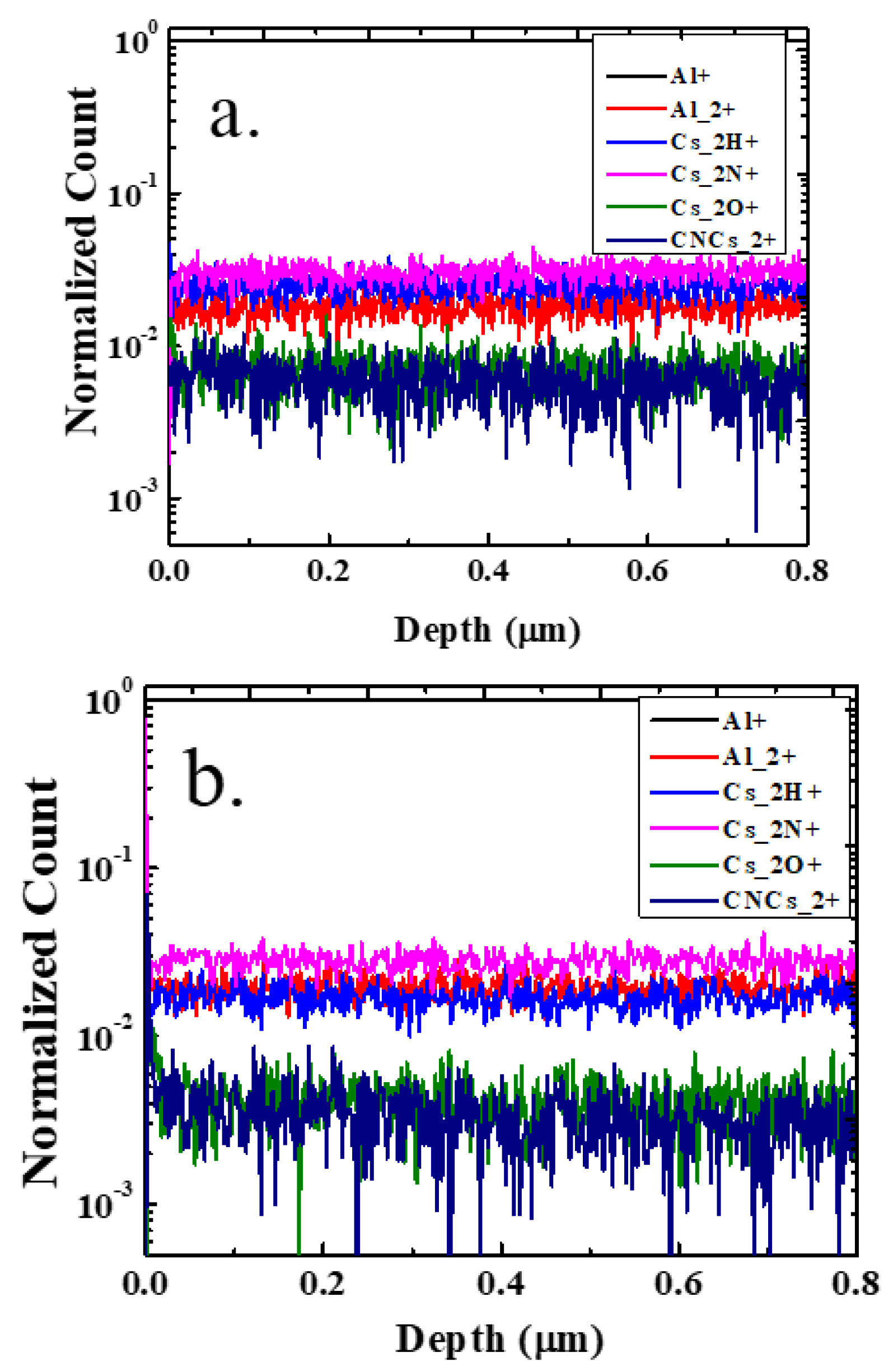
Figure 6 shows the average relative SIMS detected counts for Al2
+, Al
+, H
+, N
+, and O
+ (with respect to Al
+ normalized to (1) for both AlN samples grown with N
2 carrier and H
2 carrier gases. No significant change was observed in the composition of various compounds up to 0.8 µm (and beyond data are not shown here). The normalized count values for O
+ and C
+ in case of the sample grown using H
2 carrier gas was much less. Compared to N
2 grown samples, H
2 grown samples have 33–39% less C, 33% less H, 41% less O; a similar trend was observed in XPS analysis of these samples. The percentage difference of oxygen was close in case of SIMS and XPS measurements, but there was a difference for carbon. This may arise due to measurement techniques. Moreover, XPS measurement was taken at 5 nm depth, whereas the SIMS profile was taken up to a much higher depth.
To further understand the presence of impurities, the samples were studied by cathodoluminescence (CL). In III-nitride semiconductors near band edge emissions, such as free exciton or bound exciton recombination, are characteristics of high-quality materials with lower impurity concentration and lower defect density [
22,
23].
Figure 7 shows CL spectra of the AlN sample grown with the N
2 carrier gas, H
2 carrier gas, and the HVPE grown free-standing AlN. The peak close to 6.0 eV dominates in all the samples. Davis et al. simulated the CL spectra for aluminum gallium nitride, Al
xGa
1-xN, samples, where x is the composition of the aluminum [
24]. For x = 1, in those calculations, the pure AlN near band edge emission is close to 6.0 eV, which matches our measurements. If we closely observe these peaks, we can see that hump-like peaks are present in all the samples close to 3.8 eV, which is well known for oxygen presence [
22]. We grew our samples on sapphire substrates, so to exclude the idea that this peak can come from sapphire substrate oxygen signal, we measured the free-standing AlN grown by hydride vapor phase epitaxy (HVPE) which is from Crystal IS. We observed a peak close to the 3.8 eV for the free-standing AlN sample, confirming that the source of the oxygen-related peak was the AlN, not the sapphire substrate. In addition, the electron penetration depth was only a few nm in the AlN samples in the case of 10 kV accelerating voltage. Thus, there was less probability of incident electrons reaching the sapphire substrate. Thus, we can conclude with certainty that the source of oxygen signal was from the oxygen impurities in the AlN samples. According to Youngman et al., the luminescence peak position from oxygen-related defects in AlN shifts from 4 eV to 3.3 eV as the oxygen increased from less than 0.1 to about 0.8% [
25]. We assigned the peak at 3.8 eV, which agrees with the previously reported data [
22]. The near band edge emission (NBE) peak (~6.0 eV) peak arose from the free excitons or excitons bound to the shallow donor or acceptor impurities. The NBE peak of the samples grown with N
2 and H
2 carrier shows a blue shift with respect to HVPE grown free-standing AlN sample, which is related to stress in the MOCVD grown samples. In the next section, we evaluate the stress in these films by Raman spectroscopy measurement.
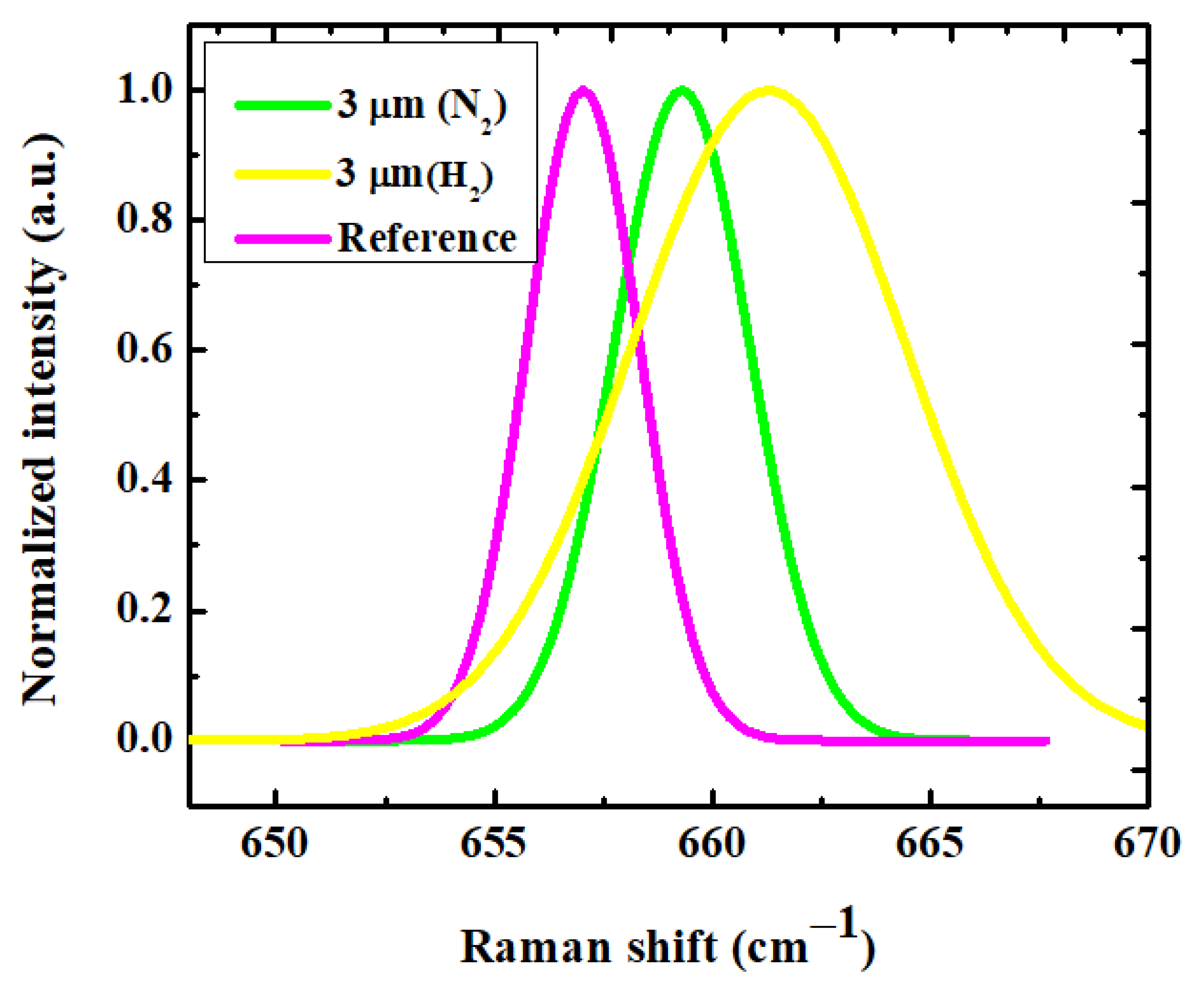
The impurities, point defects, and extended defects alter the stress values in the epitaxially grown films. Raman spectroscopy has been previously demonstrated as an effective tool to calculate stress in thin films [
26]. In the case of AlN, high-resolution phonon linewidth can provide the crystalline quality of the thin films. It has been previously reported that for single-crystal bulk AlN, the FWHM of E
2 (high) phonon mode is 3 cm
−1 [
27]. For a 3 μm AlN sample grown with N
2 carrier gas, the E
2 (high) phonon linewidth was 3.8 cm
−1; on the other hand, a 3 μm AlN sample grown with H
2 carrier was 5 cm
−1. We employed the biaxial stress coefficient to calculate stress based on the Raman shift. Biaxial stress coefficient (
) depends on the growth technique [
26]. We considered 657.04 cm
−1, the free-standing sample E
2 (high) as the stress-free frequency, and calculated the stress based on
k = −4.04 ± 0.3 cm
−1/GPa [
26].
Figure 8 shows the normalized Raman spectra of E
2(high) phonon mode where the blue shift towards the right for the grown samples indicates compressive stress. The compressive stress in AlN film results from the lattice mismatch between sapphire substrate, thermal expansion coefficient mismatch, and stress generated during the coalescence process and impurities [
28]. We have previously demonstrated that, due to the delayed coalescence, the N
2 carrier grown samples show less compressive stress [
8,
9]. The formation of voids closer to the interface for the AlN sample grown using H
2 carrier gas causes early coalescence, which leads to addition of another low temperature buffer layer to gain similar thickness and higher stress.


 ,
, 


