Abstract
A tungsten (W) material is a candidate for the first wall and silicon carbide (SiC) composites are candidates for the structural materials applied in nuclear fusion. SiC fiber-reinforced W composites are also developed for nuclear fusion applications. An effective diffusion barrier is required to prevent reaction between W and SiC. Therefore, in this work, advanced ceramics coatings, such as oxides (ZrO2, TiO2 and Er2O3), nitrides (ZrN and TiN), carbides (TiC and ZrC) were chosen to assess abilities to suppress the reactions. Various films were coated on a CVD (chemical vapor deposition)-SiC plate using the dipping method. Additionally, nitrides coatings prepared by the sputtering method were also investigated in this work. Then evaluations were carried out by joining the coated CVD-SiC plates with W foils. Only the multi-dipped Er2O3 coating and the sputtered nitrides worked well compared with the other coatings. For the other oxide coatings, reactions were identified between oxides and SiC, and for the dipped nitrides and carbides films, cracks were observed on the coating, generated from the coefficient of thermal expansion (CTE) mismatch with the SiC substrate and volume change for the oxides changing to nitrides and carbides. This work provides suggestions about choosing an appropriate interface material between SiC and W.
1. Introduction
Tungsten (W), as a metal with the highest melting point, is expected as the plasm facing material, and silicon carbide (SiC) composites are expected as the structural materials for the nuclear fusion power plant [1]. In addition, the coefficient of thermal expansion (CTE) of W and SiC is 4.6 and 4.7 × 10⁻⁶/°C, respectively. Therefore, the development of the W and SiC composites joint technology [2,3,4] or the usage of SiC to reinforce W [5,6,7] are the critical issues for the larger and more complex components in a fusion reactor. However, severe interfacial solid-state reactions happened between SiC and W after annealing at high temperature generating various carbides (WC and W2C) and silicides (W5Si3 and WSi2) [3,7,8,9]. Such produced ceramics phases damage the strength and thermal conductivity of W and SiC. Moreover, the reaction zone still exists even joined by a rapid joining method (spark plasma sintering, SPS) [2,10]. Therefore, an effective diffusion barrier is very essential for SiC and W systems to suspend the reaction.
Nevertheless, only a few works focus on diffusion barriers in SiC and W systems. It is reported that 70 nm thick TaC [11] or 100 nm thick TiN [12] can act as an effective diffusion barrier at 1000 °C, in which no reactions can be found and just grain growth after 24 h annealing. However, the evaluating temperature is much lower than the sintering temperature to fabricate the SiCf/W composites. Umber et al. [5] fabricated the TiN-coated SiC particles reinforced W materials by SPS at 1700 °C for 3 min, and the intensity of tungsten carbides and silicides’ peaks reduced a lot compared with the composite without TiN coating. However, 3 min is too short to evaluate whether it works. Roger et al. examined the TiC [13] and TiN [14] layers, and both of them can noticeably lessen the depth of the reaction zone after 1500 °C for 16 h annealing. But the thickness used in this work is thicker than 10 µm, which is too thick for interface material in a composite. Nonetheless, it’s worth investigating TiC and TiN as diffusion barriers further. ZrN and ZrC as other typical transition metal nitrides and carbides with both Ti and Zr belonging to group 4 elements, show similar properties to TiN and TiC, such as high melting point and good corrosion resistance, etc. Moreover, ZrC [15,16] or TiC [17,18] as well as ZrN [19,20] powders were added to W to remove the oxygen impurities in the grain boundary to improve the mechanical property of W, so there is evidence of good stability between carbides, nitrides and W. In addition, the thermal conductivity of these transition metal nitrides and carbides display positive trend with temperature because of high contribution of electrons [21,22,23]. Thus, ZrN and ZrC were also chosen in this work. In addition, oxides (ZrO2, TiO2 and Er2O3) with high thermal stability and low activation to irradiation [24] were selected as interface materials as well in order to suppress the movement of Si and C atom. ZrO2 powder was also used to ameliorate W’s brittleness sintered higher than 2000 °C [25]. In addition, Er2O3 acted as the interface layer in W fiber-reinforced W composites [26,27]. Thus, it’s stable between these oxides and W. Therefore, in this work, these candidate materials were chosen to assess the possibility of an effective diffusion barrier for SiC and W systems, and evaluations were carried out by SiC and W joints.
2. Materials and Methods
The dipping method might be a suitable way for coating fiber because the surface of the inner side fiber in the fiber tow can be coated easily, and on the other side, the interface between fiber and coating is not very dense, which might satisfy the weak bonding in composites to bring additional toughness by crack deflection and fiber frictional sliding to consume energy.
Seven kinds of materials oxides (ZrO2, TiO2, & Er2O3), carbides (ZrC, & TiC) and nitrides (ZrN, & TiN)) were prepared by dipping method and evaluated as diffusion barriers for SiC/W systems in this work, besides sputtering method (nitrides) were also investigated to prevent the reaction. In addition, the substrate was a CVD (chemical vapor deposition)-SiC plate in all cases instead of SiC fiber. Considering that it is convenient to coat on a plate than fiber by both dipping and sputtering method, and a joined specimen is easy to prepare and analyze the reacted thickness. Subsequently, to investigate which coating is feasible, the sandwich-like specimens were prepared by joining the coated CVD-SiC plates and W foils at 1700 °C for 1 h with 20 MPa in Ar atmosphere (see Figure 1). The uncoated CVD-SiC joined with W foils was also investigated for comparison. In addition, for the dipped diffusion barrier, each coating was dipped from once to 5-times. The used precursors to coat diffusion barrier films in this work were coating materials from Kojundo Chemical Laboratory Co., Ltd. (TIK03LB for Ti-based coating, ZRK03LB for Zr-based coating, and ERK0E1LB for Er-based coating, Saitama, Japan). The used W foils with thickness of 0.05 mm were purchased from E-metals Co., Ltd. (Osaka, Japan).
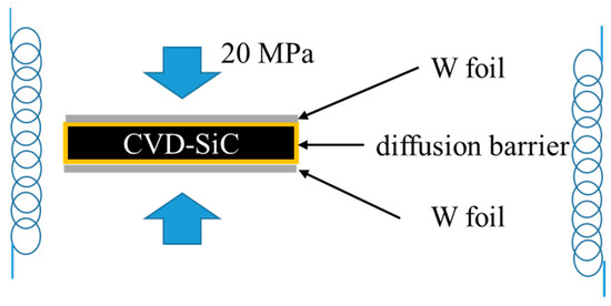
Figure 1.
Schematic diagram of W joined with diffusion barrier coated CVD-SiC.
Before joining, the dipped CVD-SiC plates were dried at 120 °C for 10 min, then annealed at 500 °C for 1 h in the air to generate oxides coating. For carbides, carbon black powders were added to the liquid precursor before dipping, then mixed well by ultrasonic treatment. Afterward, a similar condition with generating oxides was used to prepare a C dispersed oxide film. Subsequently, the coated SiC was annealed at 1600 °C for 2 h in Ar atmosphere to produce a carbide coating by a carbothermic reduction reaction. In addition, for nitrides, two kinds of methods (sputtering and dipping method), were used in this work. To produce the dipped nitrides coatings, oxide films were generated firstly. Then the oxides coated SiC plates were annealed at 1400 °C for 2 h in flowing N2. To fabricate the multiple dipped carbides and nitrides coating from oxides, high-temperature annealing was carried out every time after oxides were dipped. In addition, the sputtered nitrides coatings were generated from metals (Ti and Zr) film with about 300 nm thickness after annealing at the same condition with a dipped nitride film, which were coated at the Osaka Research Institute of Industrial Science and Technology. In addition, approximately 300 nm C is deposited firstly before the metal was coated to prevent the reactions between metals (Zr and Ti) and SiC. X-ray diffraction (XRD, Rigaku TTR-III, Tokyo, Japan) with cobalt (Co) target was carried out qualitatively for the phase analysis. The microstructure was examined by scanning electron microscope (SEM, Zeiss Ultra 55, Nagoya, Japan) in secondary electrons (SE) mode. An electron probe micro analyzer (EPMA, JEOL JXA-8500F, Tokyo, Japan) and energy-dispersive X-ray spectroscopy (EDS, EDAX, Tokyo, Japan) were used for element analysis.
3. Results
3.1. Uncoated CVD-SiC Joined with W Foil
The cross-sectional SEM image and EPMA results of the sample without diffusion barriers were shown in Figure 2. Approximately 34.5 µm average thick (measured at 5 different regions, so are the later average values) reaction layer can be observed just after 1 h heat treatment according to the image, which is almost 3-times thicker than the diameter of SiC fiber (Hi-Nicalon Type S) with 12.2 µm [28] used in SiCf/W composite [7]. It is well-known that a variety of silicides (W5Si3 and WSi2) and carbides (WC and W2C) were generated after high-temperature annealing in the W and SiC system, and the generated ceramic phases will aggravate the embrittlement of W based material. In addition, for SiCf/W composites, the interfacial reaction damaged the fiber and only a few W remained after sintering, which is detrimental to the mechanical property and thermal conductivity of the composite. Therefore, an effective diffusion barrier is vitally important.
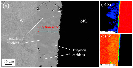
Figure 2.
The cross-sectional SEM image with secondary electron mode (image (a)) and element distribution by EPMA (image (b) for Si; image (c) for W.) of joined CVD-SiC and W foil without diffusion barriers at 1700 °C, 20 MPa for 1 h.
3.2. CVD-SiC and W Foil Joined with Diffusion Barrier
3.2.1. Oxide Coatings
XRD patterns of dipped oxides films are shown in Figure 3, and the results indicate that 3 kinds of oxides were indeed produced after heat treatment at 500 °C. Furthermore, the other unmarked peaks in Figure 3 belong to CVD-SiC. In addition, the obtained TiO2 showed anatase structure based on XRD data. The SEM images of the oxide coatings’ surface and cross-section coated on SiC were shown in Figure 4. It is easy to observe the cracks on the surface of ZrO2 coating and TiO2 coating due to the large CTE mismatch with SiC (4.7 × 10⁻⁶/K), and the CTE (coefficient of thermal expansion) of ZrO2 and A-TiO2 (anatase TiO2) were 9.6 × 10⁻⁶/K and 17.35 × 10⁻⁶/K (c-axis) [29] at room temperature, respectively. In addition, almost no cracks can be found on the surface of Er2O3 coating, caused by a suitable CTE value of 7.25 × 10⁻⁶/K [30]. From images (d–f) in Figure 4, it can be found that the thickness of dipped oxides coating is about 100–200 nm for a 1-time dipping.
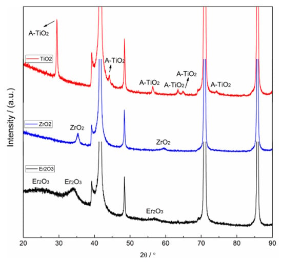
Figure 3.
XRD patterns of oxides coating on CVD-SiC substrate after 1-time dipping. Black is for Er2O3 coating; Blue is for ZrO2 coating; Red is TiO2 coating.
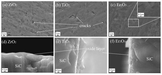
Figure 4.
Surface and cross-sectional SEM images of oxides coating on CVD-SiC substrate after 1-time dipping before joining with SE2 mode. (a,d) are the images of surface and cross-section of 1-time dipped ZrO2 coating, respectively; (b,e) are the images of surface and cross-section of 1-time dipped TiO2 coating, respectively; (c,f) are the images of surface and cross-section of 1-time dipped Er2O3 coating, respectively.
Figure 5 exhibits the cross-sectional images of dipped oxides-coated CVD-SiC and W after joining. The reaction zone (RZ) between W and SiC still can be observed in specimens with oxides coating. Moreover, the depth of RZ in ZrO2 and TiO2-coated specimens were approximately 33 µm and 40 µm, respectively, which is almost the same thickness of RZ compared with the joined sample without the diffusion barrier (see Figure 2), indicating that dipped ZrO2 and TiO2 coating were noncontributing as diffusion barriers in the W and SiC system. When regarding the joined specimen with a dipped Er2O3 coating, the thickness of the RZ is about 28 µm, thinner than the RZ of the non-interface sample and the other oxides film cases, revealing that Er2O3 might be suitable material for the W/SiC system. Thus, the influence of the Er2O3 coatings’ thickness on whether diffusion barrier works was examined further, and the thickness was modified by the number of dips. The images of the surface and cross-section of multi-dipped Er2O3 coating (from 2-times to 5-times) before and after joining were shown in Figure 6, manifesting the impact of thickness of diffusion barrier. The thickness of Er2O3 film increased from 115 nm (see Figure 4f) by 1-time dipping to approximately 550 nm (see Figure 6d,f) by 5-times dipping. After 3-times dipping with about 300 nm thick Er2O3 layer, the depth of RZ reduced by 72% for the specimen without a diffusion barrier and 67% for the specimen with 1-time dipped Er2O3 coating, respectively. At the same time, only about 1.1 µm thick (thickest part) reaction layer can be found in the joined specimen with about 500 nm thick Er2O3 film, although there are still some cracks about 1µm in length, generated in the last time dipping period, which can be observed on the surface of the multi-dipped film (see Figure 6e).
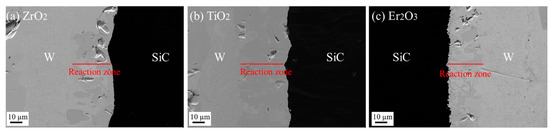
Figure 5.
SEM images of cross-section of W joined with dipped oxide-coated SiC by 1-time dipping after 1700 °C, 20 MPa for 1 h heat treatment. (a) Cross-sectional image of dipped ZrO2-coated SiC joined with W; (b) Cross-sectional image of dipped A-TiO2-coated SiC joined with W; (c) Cross-sectional image of dipped Er2O3-coated SiC joined with W.
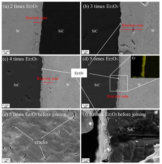
Figure 6.
SEM images of surface and cross-section of coated CVD-SiC before and after joining with W foils. Images (a–d) are the cross-section of 2-times to 5-times dipped Er2O3-coated SiC joined with W, respectively; (e) is surface of Er2O3 coating by 5-times dipping before joining; (f) is cross-section of Er2O3 coating by 5-times dipping before joining.
3.2.2. Carbide Coatings
Carbides in this work were produced by carbothermal reduction reactions between oxides and carbon black as follows.
ZrO2 + 3C = ZrC + 2CO,
TiO2 + 3C = TiC + 2CO
XRD data of carbides film coated on CVD-SiC by the dipping method are displayed in Figure 7, fabricated after annealing at 1600 °C for 2 h in a flowing Ar atmosphere. The results demonstrate that carbides were generated, and the peaks of the carbides became strong with a number of dips, revealing that the thickness and crystallinity of carbides increased with the number of dips. Because the total heat treatment time for 5-times dipped coating was 10 h. Additionally, a longer annealing time also caused the grain growth (see Figure 8).
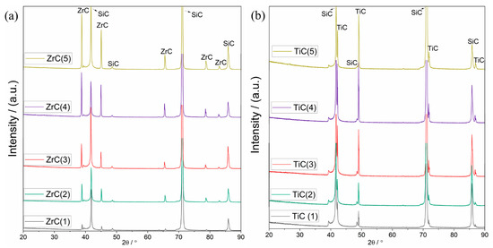
Figure 7.
XRD patterns of carbides by dipping method before joining. (a) ZrC; (b) TiC.
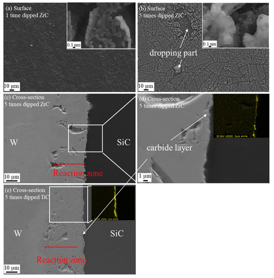
Figure 8.
The surface and cross-sectional SEM images of dipped carbides film coated SiC before and after joining. (a) the surface of 1-time dipped ZrC coated SiC before joining, (b) the surface of 5-times dipped ZrC-coated SiC before joining, (c) 5-times dipped ZrC coated SiC joined with W; (d) 5-times dipped ZrC-coated SiC joined with W with larger magnification; (e) 5-times dipped TiC-coated SiC joined with W.
Figure 8 displays the SEM images of the surface of the carbide film by dipping method and cross-sectional interface of diffusion barrier coated CVD-SiC and W foil after high temperature annealing with 20 MPa pressure. The 5-times dipped carbides films were prepared by dipping and then annealed at 1600 °C 5 times. It can be observed the thickness of the ZrC was just about 323 nm, thinner than the other 5-times dipped films, indicating that part of ZrC film peeled off. This is because the volume change occurred during the reaction process, causing from the higher density of carbides ZrC (6.73 g/cm3) and TiC (4.93 g/cm3) than oxides (ZrO2 (5.68 g/cm3) and TiO2 (4.23 g/cm3)). Such volume variations leaded to thermal stress then generating cracks on the surface in the procedure from oxides to carbides. Thus, the larger volume changes in ZrC coating lead to the phenomenon of stripping (see Figure 8b). However, the CTE of ZrC of 7.5 × 10⁻⁶/K is less than TiC of 8.5 × 10⁻⁶/K [22], implying that the volume changes caused by the difference in density dominate the procedure. Moreover, a similar phenomenon can be observed in a multiple-dipped nitrides coating. However, the width of RZ in the TiC-coated case was almost the same as the RZ in the ZrC-coated sample although the thickness of TiC film with around 808 nm in the relatively thicker part is more than twice of ZrC coating, implying the ZrC might be more effective than TiC as a diffusion barrier in W/SiC. However, ZrC produced by dipping method using carbothermic reduction is not appropriate due to film peeling off for the reason of the big difference in density. Thus, it is better to minimize the steps of producing carbide film as possible or coat the diffusion barrier on fiber directly.
3.2.3. Nitride Coatings
Dipped Nitride Coatings
XRD patterns of nitrides coating produced by dipping several times and annealing at 1400 °C for 2 h in a flowing N2 atmosphere are displayed in Figure 9. The results show nitrides can be produced by annealing in N2. Moreover, no other reaction products were identified after heat treatment. Additionally, similar to multi-dipped carbides coating, the intensity of the nitrides’ peaks became stronger with the dipping times, suggesting that 5 times dipped nitrides coatings have better crystallinity, which is similar to the carbide cases.
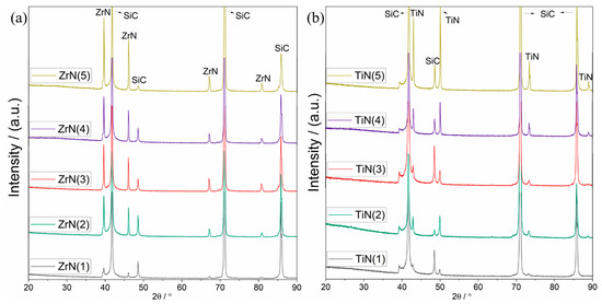
Figure 9.
XRD patterns of nitrides by dipping method before joining. (a) ZrN; (b) TiN.
Figure 10 displays the surface of nitrides film by dipping method before joining and the cross-sectional images of 5-times dipped nitrides coated SiC joined with W foil. It is easy to recognize the grain growth after several times dipping, and the grain size in the 5-times TiN film is about 250 nm, which is approximately 3 times compared with the 1-time dipping case with the grain size lower than 100 nm, matching with the XRD results and similar with the carbide case. In addition, after joining with W at high temperature, the thickness of RZ in TiN coating prepared by 5-times dipping case is about 13.6 µm, much lower than the specimen without diffusion barrier with 33 µm RZ and 5-times dipped ZrN coating specimen. However, the width of RZ in the dipped TiN diffusion barrier is almost 10-times thicker compared with the Er2O3-coated specimen (see Figure 6d and Figure 10c), which suggests that Er2O3 exhibits the most efficient diffusion barrier for coatings prepared by the dipping method.
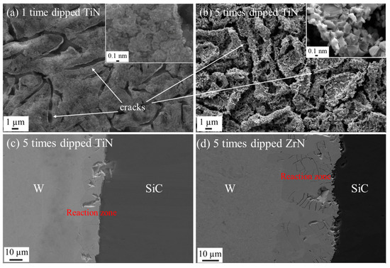
Figure 10.
The surface and cross-sectional SEM images of dipped nitride coated SiC before and after joined with W foil at 1700 °C with 20 MPa pressure. (a) the surface of 1-time dipped TiN on CVD-SiC with different magnifications; (b) the surface of 5-times dipped TiN film; (c) the cross-sectional of 5 times dipped TiN-coated SiC joined with W; (d) the cross-sectional of 5-times dipped ZrN-coated SiC joined with W.
Sputtered Nitride Coatings
The ZrN and the TiN produced by a sputtering method, acting as diffusion barriers in SiC and W systems, were also studied. The sputtered nitrides coating in this work was from the metal Zr or Ti film annealed at the same condition with the dipped nitride coating, namely 1400 °C in an N2 atmosphere for 2 h [6]. Carbon here is to protect SiC from Ti and Zr metal during the nitrides producing process. Figure 11 exhibits the SEM image of the surface and cross-section of the sputtered metal films before annealing. The thickness of the C and metal layer are about 300 nm, respectively. And the dense metal coatings were fabricated by a sputtering method according to the SEM images of the surface and cross-section.
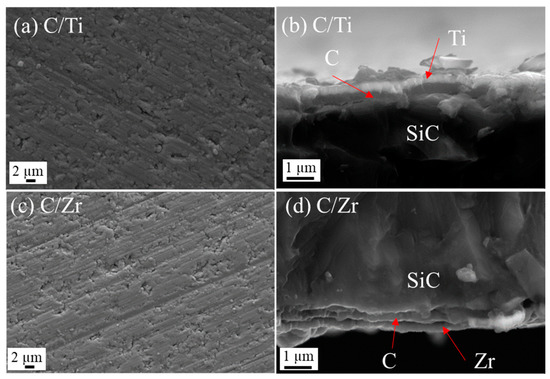
Figure 11.
SEM images of surface and cross-section of sputtered coating with SE2 mode before heat treatment. (a,b) are the surface and cross-sectional image of sputtered C/Ti coating, respectively; (c,d) are the surface and cross-sectional image of sputtered C/Zr coating, respectively.
The surface and cross-sectional SEM images of sputtered metal films after 1400 °C heat treatment are displayed in Figure 12. The nitrides were indeed generated by annealing in N2 in terms of the XRD results (see Figure 12b). In addition, some microcracks, caused by the volume change during annealing and CTE mismatch between C and nitrides, were observed on the surface, but the length and width of the cracks on the sputtered coating were much smaller than that of the dipped film (see Figure 10a,b) and Figure 12d). Moreover, the TiN coating surface had a similar microstructure to the ZrN coating.
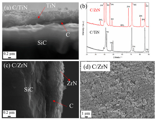
Figure 12.
SEM images with SE2 mode of surface and cross-section of sputtered coating and XRD patterns after 1400 °C heat treatment at N2 atmosphere. (a) the cross-sectional image of C/TiN coating; (b) XRD patterns of sputtered coating after 1400 °C heat treatment; (c) the cross-sectional image of C/ZrN coating; (d) the surface of C/ZrN coating.
The joining condition is the same as the dipped specimens, and the evaluated results of sputtered nitrides as diffusion barriers are displayed in Figure 13. The thickness of RZ for both nitrides coating was much thinner for the comparison with the specimen without interface coating and dipped films coated specimen (except dipped Er2O3 coating), although some cracks can be noticed on the surface of sputtered nitrides coating, implying the nitrides fabricated by the sputtering method were good candidates for diffusion barrier application for SiC/W system, while the dipped nitrides did not work well. A phenomenon that needs to be noticed here is that the reaction zone in the TiN-coated specimen identified by SEM and EPMA was located in the inner part of W, rather than the junction area, which may cause from the cracks in the W foil (see Figure 13a). Figure 14 exhibits the line scan results of SiC/TiN/W joint, which also confirm the occurrence.
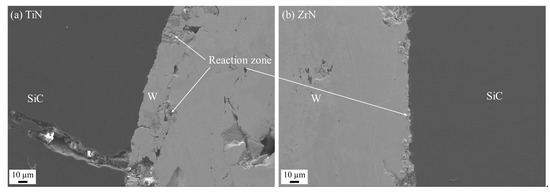
Figure 13.
SEM images and EPMA results of cross-section of sputtered coated SiC joined with Wfoils. (a) cross-sectional SEM images of TiN-coated SiC and W; (b) cross-sectional SEM images of ZrN-coated SiC and W.
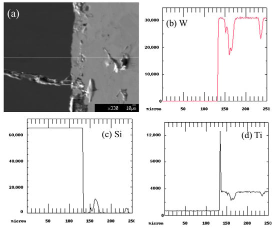
Figure 14.
Line scan results of TiN-coated SiC joined with W by EPMA. (a) line scanned area; (b) W; (c) Si; (d) Ti.
4. Discussion
The summary results are described in Table 1. The carbides and nitrides coating fabricated by dipping method from the dipped oxides film annealed at high temperature (1600 °C for carbides, and 1400 °C for nitrides) induced larger thermal stress leading to more and larger cracks due to the high-temperature processing compared with the temperature producing oxides film (500 °C). Additionally, large volume shrinkage caused by phase transition creates more enormous cracks, revealing that the dipped nitrides and carbides were not appropriate as diffusion barriers. Thus, the dipped carbides and nitrides film eventually failed. On the other hand, the sputtered nitrides film, by annealing metals in N2 atmosphere, can successfully impede the reaction. The different methods (dipping and sputtering) also caused the varying results. In addition, the joining process (SPS [5] and hot-press) has an effect on whether diffusion barriers work even at the same temperature resulting from the holding time of 3 min for SPS in [5] and 1 h for the hot press in this work. Shorter holding times can reduce the thickness of the reaction zone. Thus, whether the carbides are suitable needs to be further studied, although the dipped film cannot work well.

Table 1.
The results of SiC/W joints with different diffusion barrier coatings joined at 1700 °C for 1 h.
The Er2O3 show the best results among oxides coatings. In addition, to understand the reaction between SiC and the oxide coating directly, the dipped oxide coatings were annealed at 1600 °C without the W foils, and the results are revealed in Figure 15. The severe reactions were observed in ZrO2 and TiO2, and the surface of ZrO2 and TiO2 coated SiC became very rough and uneven. From the results of the spot scan in the ZrO2-coated SiC in Figure 15, the peak of Zr was identified just in the bright part, namely area 1. Thus, ZrC was formed in this zone after high-temperature annealing. The dark zone is SiC rich region. Although for the dipped Er2O3 coating, only grain growth can be noticed, and the dipped Er2O3 film still exhibited relatively uniform in contrast with the others. Thus, the Er2O3 layer as diffusion barriers in the composites merits further study. However, ZrO2 and TiO2 cannot be used as the interface in the SiCf/W composites for the damage of fiber due to the reaction between oxides and SiC.
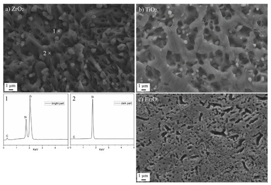
Figure 15.
SEM images and EDS (spot scan) of dipped oxides coating after 1600 °C, 2 h annealing. (a) ZrO2; (b) TiO2; and (c) Er2O3.
5. Conclusions
Seven materials (oxides (ZrO2, TiO2, and Er2O3), carbides (ZrC and TiC), and nitrides (ZrN and TiN) produced by the dipping or sputtering method as candidate diffusion barriers in W and SiC system were investigated using CVD-SiC and W foil joints in this work. According to these results, the potential diffusion barrier materials are Er2O3, ZrN, and TiN. Moreover, the methods used to prepare the coatings have a great impact on the consequences. In addition, the ZrO2 and TiO2 are not appropriate due to the reactions between SiC and these oxides. For the carbides, films prepared by dipping are not suitable. On the other hand, carbides produced by other methods need to be investigated further.
Author Contributions
Conceptualization, Y.D. and T.H.; methodology, Y.D.; investigation, Y.D., B.W. and Y.Z.; writing—original draft preparation, Y.D.; writing—review and editing, B.W., Y.Z. and T.H.; supervision, T.H.; funding acquisition, T.H. All authors have read and agreed to the published version of the manuscript.
Funding
This research was funded by JSPS KAKENHI Grant Number 21H01063.
Institutional Review Board Statement
Not applicable.
Informed Consent Statement
Not applicable.
Data Availability Statement
Not applicable.
Acknowledgments
The authors wish to thank Yusuke Kondo at Osaka Research Institute of Industrial Science and Technology, Japan to help coating the sputtered films.
Conflicts of Interest
The authors declare no conflict of interest.
References
- Koyanagi, T.; Katoh, Y.; Nozawa, T.; Snead, L.L.; Kondo, S.; Henager, C.H.; Ferraris, M.; Hinoki, T.; Huang, Q. Recent progress in the development of SiC composites for nuclear fusion applications. J. Nucl. Mater. 2018, 511, 544–555. [Google Scholar] [CrossRef]
- Li, H.X.; Zhong, Z.H.; Zhang, H.B.; Zhu, Z.X.; Hua, P.; Chen, C.; Wu, Y.C. Microstructure characteristic and its influence on the strength of SiC ceramic joints diffusion bonded by spark plasma sintering. Ceram. Int. 2018, 44, 3937–3946. [Google Scholar] [CrossRef]
- Son, S.J.; Park, K.H.; Katoh, Y.; Kohyama, A. Interfacial reactions and mechanical properties of W-SiC in-situ joints for plasma facing components. J. Nucl. Mater. 2004, 329–333, 1549–1552. [Google Scholar] [CrossRef]
- Kishimoto, H.; Shibayama, T.; Shimoda, K.; Kobayashi, T.; Kohyama, A. Microstructural and mechanical characterization of W/SiC bonding for structural material in fusion. J. Nucl. Mater. 2011, 417, 387–390. [Google Scholar] [CrossRef]
- Umer, M.A.; Lee, D.; Waseem, O.A.; Ryu, H.J.; Hong, S.H. Fabrication of protective-coated SiC reinforced tungsten matrix composites with reduced reaction phases by spark plasma sintering. Met. Mater. Int. 2016, 22, 493–500. [Google Scholar] [CrossRef]
- Shi, X.; Wang, M.; Zhang, S.; Zhang, Q. Fabrication and properties of W-20Cu alloy reinforced by titanium nitride coated SiC fibers. Int. J. Refract. Met. Hard Mater. 2013, 41, 60–65. [Google Scholar] [CrossRef]
- Du, Y.; Hinoki, T. Effect of tungsten matrix on the mechanical property of SiC fiber reinforced tungsten composites with foils fabricated at 1700 °C. Nucl. Mater. Energy 2022, 31, 101142. [Google Scholar] [CrossRef]
- Seng, W.F.; Barnes, P.A. Calculations of cobalt suicide and carbide formation on SiC using the Gibbs free energy. Mater. Sci. Eng. B Solid-State Mater. Adv. Technol. 2000, 76, 225–231. [Google Scholar] [CrossRef]
- Kang, H.K. Microstructures of high volume SiC reinforced tungsten composites produced by plasma spray. Scr. Mater. 2004, 51, 1051–1055. [Google Scholar] [CrossRef]
- Hinoki, T.; Snead, L.L.; Blue, C.A. Development of refractory armored silicon carbide by infrared transient liquid phase processing. J. Nucl. Mater. 2005, 347, 207–216. [Google Scholar] [CrossRef]
- Wang, Z.; DelaCruz, S.; Tsai, D.S.; Maboudian, R. W/TaC/SiC sandwich stack for high temperature applications. Ceram. Int. 2019, 45, 22292–22297. [Google Scholar] [CrossRef]
- DelaCruz, S.; Wang, Z.; Cheng, P.; Carraro, C.; Maboudian, R. TiN diffusion barrier for stable W/SiC(0001) interfaces in inert ambient at high temperature. Thin Solid Films 2019, 670, 54–59. [Google Scholar] [CrossRef]
- Roger, J.; Audubert, F.; le Petitcorps, Y. Thermal stability of W-xRe/TiC/SiC systems (x = 0, 5 and 25 at % Re) at high temperature. Adv. Eng. Mater. 2009, 11, 399–407. [Google Scholar] [CrossRef]
- Roger, J.; Audubert, F.; Le Petitcorps, Y. Reactivity of M/TiN/SiC systems (M = W and Mo) at high temperature. J. Mater. Sci. 2010, 45, 3073–3079. [Google Scholar] [CrossRef]
- Golestani Fard, M.A.; Baharvandi, H. Development of W–ZrC composite coating on graphite by a TIG-aided surface cladding process. Ceram. Int. 2021, 47, 27958–27971. [Google Scholar] [CrossRef]
- Liu, R.; Xie, Z.M.; Yang, J.F.; Zhang, T.; Hao, T.; Wang, X.P.; Fang, Q.F.; Liu, C.S. Recent progress on the R&D of W-ZrC alloys for plasma facing components in fusion devices. Nucl. Mater. Energy 2018, 16, 191–206. [Google Scholar] [CrossRef]
- Xie, X.F.; Jing, K.; Xie, Z.M.; Liu, R.; Yang, J.F.; Fang, Q.F.; Liu, C.S.; Wu, X. Mechanical properties and microstructures of W–TiC and W–Y2O3 alloys fabricated by hot-pressing sintering. Mater. Sci. Eng. A 2021, 819, 141496. [Google Scholar] [CrossRef]
- Kurishita, H.; Matsuo, S.; Arakawa, H.; Sakamoto, T.; Kobayashi, S.; Nakai, K.; Takida, T.; Kato, M.; Kawai, M.; Yoshida, N. Development of re-crystallized W-1.1%TiC with enhanced room-temperature ductility and radiation performance. J. Nucl. Mater. 2010, 398, 87–92. [Google Scholar] [CrossRef]
- Lee, D.; Umer, M.A.; Shin, Y.; Jeon, S.; Hong, S. The effect of sintering conditions and ZrN volume fraction on the mechanical properties of spark plasma sintered W/ZrN composites. Mater. Sci. Eng. A 2012, 552, 481–485. [Google Scholar] [CrossRef]
- Kim, M.; Kim, S.; Kang, J.; Song, S.H.; Lee, D. Effects of ZrN and W Particle Sizes on the Mechanical and Ablation Properties of ZrN/W Composites. Met. Mater. Int. 2019, 25, 733–739. [Google Scholar] [CrossRef]
- Adachi, J.; Kurosaki, K.; Uno, M.; Yamanaka, S. Thermal and electrical properties of zirconium nitride. J. Alloys Compd. 2005, 399, 242–244. [Google Scholar] [CrossRef]
- Lengauer, W. Transition Metal Carbides, Nitrides, and Carbonitrides. Handb. Ceram. Hard Mater. 2008, 265, 202–252. [Google Scholar] [CrossRef]
- Harrison, R.W.; Lee, W.E. Processing and properties of ZrC, ZrN and ZrCN ceramics: A review. Adv. Appl. Ceram. 2016, 115, 294–307. [Google Scholar] [CrossRef]
- Chikada, T.; Suzuki, A.; Yao, Z.; Sawada, A.; Terai, T.; Muroga, T. Basic study on self-healing of Er2O3 coating for vanadium-lithium blanket system. Fusion Eng. Des. 2007, 82, 2572–2577. [Google Scholar] [CrossRef][Green Version]
- Xiao, F.; Miao, Q.; Wei, S.; Li, Z.; Sun, T.; Xu, L. Microstructure and mechanical properties of W-ZrO2 alloys by different preparation techniques. J. Alloys Compd. 2019, 774, 210–221. [Google Scholar] [CrossRef]
- Jasper, B.; Schoenen, S.; Du, J.; Hoeschen, T.; Koch, F.; Linsmeier, C.; Neu, R.; Riesch, J.; Terra, A.; Coenen, J.W. Behavior of tungsten fiber-reinforced tungsten based on single fiber push-out study. Nucl. Mater. Energy. 2016, 9, 416–421. [Google Scholar] [CrossRef]
- Riesch, J.; Buffiere, J.Y.; Höschen, T.; Scheel, M.; Linsmeier, C.; You, J.H. Crack bridging in as-fabricated and embrittled tungsten single fibre-reinforced tungsten composites shown by a novel in-situ high energy synchrotron tomography bending test. Nucl. Mater. Energy 2018, 15, 1–12. [Google Scholar] [CrossRef]
- Morimoto, T.; Ogasawara, T. Potential strength of NicalonTM, Hi NicalonTM, and Hi Nicalon Type STM monofilaments of variable diameters. Compos. Part A Appl. Sci. Manuf. 2006, 37, 405–412. [Google Scholar] [CrossRef]
- Hummer, D.R.; Heaney, P.J.; Post, J.E. Thermal expansion of anatase and rutile between 300 and 575 K using synchrotron powder X-ray diffraction. Powder Diffr. 2007, 22, 352–357. [Google Scholar] [CrossRef]
- Dargis, R.; Williams, D.; Smith, R.; Arkun, E.; Roucka, R.; Clark, A.; Lebby, M. Structural and Thermal Properties of Single Crystalline Epitaxial Gd2O3 and Er2O3 Grown on Si(111). ECS J. Solid State Sci. Technol. 2012, 1, N24–N28. [Google Scholar] [CrossRef]


Publisher’s Note: MDPI stays neutral with regard to jurisdictional claims in published maps and institutional affiliations. |
© 2022 by the authors. Licensee MDPI, Basel, Switzerland. This article is an open access article distributed under the terms and conditions of the Creative Commons Attribution (CC BY) license (https://creativecommons.org/licenses/by/4.0/).