Abstract
The barrier properties and diffusion behavior of Cu(Re) alloy films were studied. The films were deposited onto barrierless SiO2/Si by magnetron sputtering. X-ray diffraction patterns and electric resistivity results proved that the Cu(Re) alloy films without a barrier layer were thermally stable up to 550 °C. Transmission electron microscopy images and energy-dispersive spectrometry employing scanning transmission electron microscopy provided evidence for a self-formed Re-enriched diffusion layer between the Cu(Re) alloy and SiO2/Si substrate. Furthermore, the chemical states of Re atoms at the Cu(Re)/SiO2 interface were analyzed by X-ray photoemission spectroscopy. The self-formed diffusion layer was found to be composed of Re metal, ReO, ReO2 and ReO3. At 650 °C, the Cu(Re) layer was completely destroyed due to atom diffusion. The low electrical resistivity in combination with the high thermal stability suggests that the Cu(Re) alloy could be the ultimate Cu interconnect diffusion barrier.
1. Introduction
To avoid rapid copper diffusion in integrated circuits (ICs), Cu interconnects require an effective barrier to prevent interdiffusion or reaction between the Cu and adjoining materials [1,2,3,4,5]. Various refractory metals and their nitride diffusion barriers, such as Ti, Ta, Ru and Mn, which have a low electrical resistivity, high stability and good interface adhesion, are in high demand [6,7,8,9]. To avoid the undesired formation of high-resistivity copper silicide, an ultra-thin Cu diffusion barrier with excellent barrier performance and low interconnect resistivity is needed to enhance IC performance [10,11]. The continuous scaling down of ICs to a few-nanometer regime has led to the issue of fabricating an ultra-thin barrier layer with step coverage on the sidewalls and bottom corners of trenches and vias [12]. Moreover, barrier layers occupy an increasing fraction at the cross-sectional area of conductors, leading to an increase in the electrical resistivity of the Cu interconnects [4]. Therefore, it is urgent to explore alternative methods of removing barrier layers which will also reduce the manufacturing cost using simplified technology.
Due to the difficulty in achieving uniform depositions of ultra-thin barrier layers, more attention has been paid to self-formed diffusion barriers (barrierless metallization) in recent years [13,14,15]. The self-formed barrier layer offers low electrical resistivity, resistance to Cu diffusion, resistance to electromigration and compatibility with conformal deposition techniques [16,17,18,19,20,21]. A self-formed barrier scheme is achieved by doping with diffusion barrier elements as well as their nitrides and carbides, such as Ti, Zr, Mn and WN [22,23,24,25,26,27,28]. All these doped elements have low-concentration solutes in Cu, which are supposed to segregate at the interface as a diffusion layer during annealing [16,29]. The thin self-formed layer at the interface acts as an adhesion and diffusion barrier layer. Due to the high melting point, strong bonding to resist interdiffusion and low (almost zero) solubility of Cu for an easy phase separation, Re might be a potential alloying element for barrierless metallization [6,30]. Chang et al. reported that the electroless-plated Cu(Re) alloy can serve as a barrierless metallization material to prevent Cu diffusion [6]. The mechanism of influences that Re might have on the diffusion-hindering behavior should be further studied. In the present study, rather than focusing on the influence of preparation methods on the barrier property, attempts were mainly made to provide more detailed information to clarify the growth mechanism of Re self-formed barrier layers, which will be used in the composition design of Cu–Re alloy film compositions.
2. Experimental
(111)-oriented Si wafers with a ~20 nm-thick oxidized SiO2 layer were used as substrates (Lijing, Wenzhou, Wenzhou, China). The substrates were cleaned successively by ultrasonication in acetone and ethanol for 20 min. After drying with ultra-high purity N2 gas, the substrates were immediately loaded into the sputtering system. Before deposition, the target and Re chips were pre-sputtered for 10 min to remove the impurities and oxide layers. Cu(Re) thin films were deposited on the SiO2/Si substrates using a direct current (DC) magnetron sputtering system (Sky Technology development, Shenyang, China). The Cu films with ~2.3 at.% Re were obtained by co-sputtering the Cu target and Re chips (Ketai, Nanchang, China). Pure Re chips (99.99%, 5 mm × 5 mm) were pasted onto a pure Cu target (99.999%, diameter of 75 mm × thickness of 5 mm). The deposition was carried out at a background pressure of 5 × 10⁻⁴ Pa and an Ar gas deposition pressure of 1 Pa, with a target power of 100 W. The substrates were not heated during deposition, and the thickness of the Cu(Re) thin film after the deposition was about 150 ± 10 nm.
Isothermal annealing was performed in vacuum at a pressure of 6 × 10⁻⁵ Pa for 30 min, at temperatures ranging from 350 to 650 °C. Characterization of the phase composition and crystalline structure of the samples was determined by X-ray diffraction (XRD; D8 Venture, Bruker, Billerica, MA, USA) in the 2θ = 40°–70° range at a step size of 0.04°. The four-point probe (FPP; ST2258C, JingGe, Suzhou, China) method was used to measure the sheet resistance of the films before and after annealing. The interfacial behavior of the films was investigated by cross-section transmission electron microscopy at 200 kV (TEM; JEM2100F, JEOL, Tokyo, Japan). The cross-section TEM samples were ground with SiC paper until the total thickness obtained was about 50–100 µm and then thinned down to electron transparency by an Ion Polishing System (Gatan, Pleasanton, CA, USA). The component distribution of the Cu(Re)/SiO2/Si films was analyzed by EDX-STEM (energy-dispersive spectrometry employing scanning transmission electron microscopy). The EDX-STEM instrument used was a JEM2100F operated at 200 kV and equipped with a solid-state X-ray detector (HAADF—high-angle annular dark field). EDX spectrum images were acquired with Oxford AZtec software (version 3.1) using the X-MaxN detector system with a dwell time of 30 μs and a typical image size of 512 × 512 pixels. The X-ray photoelectron spectroscopy measurement (XPS, PHI 5000, VersaProbeIII, ULVAC-PHI, Chigasaki, Japan) was carried out on the Ar-ion-sputtered film surface at the beam energy of 1.5 keV. During the test, the photoelectron take-off angle was 45°, monochromated Al Kα (1486.6 eV) was used as the X-ray source and the X-ray beam surveyed 100 μm. In the binding energy (BE) analysis, a correction was made by aligning the peak positions with reference to the standard adventitious carbon peak (C1s) at 284.8 eV.
3. Results and Discussion
Figure 1a presents the XRD analysis which was performed to investigate the phase evolutions of Cu(Re)/SiO2/Si and Cu/SiO2/Si samples before and after annealing at various temperatures. The 2θ diffraction peaks were found at 43.11° and 50.26°, corresponding to Cu (111) and Cu (200) for the as-deposited sample, as indexed in Figure 1a. No peaks corresponding to copper silicide were observed for the samples annealed at 350–550 °C. However, when the annealing temperature was increased to 650 °C, the existence of copper silicide was confirmed by the diffraction peaks related to Cu3Si (012) and Cu3Si (300). The presence of copper silicide indicates that Cu had diffused and reacted with the SiO2/Si substrate. However, the formation of Cu3Si was detected at 350 °C for the pure Cu on SiO2/Si, implying a total failure of the copper metallization layer. The evolution of the sheet resistance as a function of annealing temperatures is plotted in Figure 1b. The resistivity of the as-deposited Cu(Re) film was found to be 6.41 μΩ·cm, higher than that of the pure Cu films (5.17 μΩ·cm) [12]. The resistivity of Cu(Re)/SiO2/Si stacks slightly decreased to 5.89 μΩ·cm after annealing at 350 °C. This decrease was attributed to defect annihilation and stress relief in the film during annealing [31]. Then, it increased slowly at a temperature range of 350–550 °C. According to the XRD results, highly resistant copper silicide was not detected. Thus, the slight increase in the resistivity could be due to the Re segregation at the surface and interface that prevents the diffusion of the Cu atoms into the substrate [32]. A dramatic increase in resistivity was observed at 650 °C, as shown in Figure 1b. The increase in the sheet resistance indicated the rapid interdiffusion of copper and silicon toward the interface, finally leading to the formation of copper silicide, as observed in the XRD results. The above results prove that the Cu(Re)/SiO2/Si interconnect structure can improve thermal stability against Cu diffusion even at 550 °C, which suggests that Re is a good candidate for use as a barrier alloy.
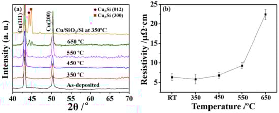
Figure 1.
(a) The phase evolutions for Cu(Re)/SiO2/Si annealed at various temperatures and Cu/SiO2/Si annealed at 350 °C. (b) Electrical results for Cu(Re)/SiO2/Si samples before and after annealing at various temperatures.
To further observe the interface diffusion behavior, typical TEM cross-sectional images of the Cu(Re)/SiO2/Si interconnect structure are displayed in Figure 2. Figure 2a reveals a uniform thickness of ~150 nm for the Cu(Re) layer with a columnar grain and a ~20 nm amorphous SiO2 layer for the as-deposited sample. Flat and free of intermixing, Cu/SiO2 and SiO2/Si interfaces were clearly revealed. The interconnect structure of the samples annealed at 350 and 450 °C remained unchanged compared with that of the as-deposited sample. The columnar structure of the Cu(Re) layer was maintained, and no considerable grain growth was observed during annealing due to the presence of Re. No obvious formation of copper silicide was observed in Figure 2b,c. With a further increase in the annealing temperature to 550 °C, atom diffusion eliminated the column grain structure of the Cu(Re) layer, as depicted in Figure 2d. Moreover, the Cu(Re) layer no longer maintained its columnar structure. As shown in Figure 2e, the Cu layer did not retain its lateral integrity in the sample annealed at 650 °C. As seen in Figure 2e, the ~55 nm Cu(Re) layer was destroyed by atom diffusion. It is worth noting that a self-formed layer existed at the Cu(Re)/SiO2 interface, as indicated in Figure 2e, which was revealed in the following EDX-STEM and XPS analysis.
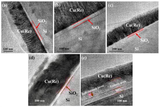
Figure 2.
TEM cross-sectional images of the Cu(Re)/SiO2/Si interconnect structure at various temperatures: (a) as-deposited, (b) 350 °C, (c) 450 °C, (d) 550 °C and (e) 650 °C.
The high-resolution cross-sectional TEM (HRTEM) images of the interfaces for the Cu(Re)/SiO2/Si structure are depicted in Figure 3. Clear interfaces were observed in the as-deposited Cu(Re)/SiO2/Si interconnect structure, as shown in Figure 3a. The Cu layer and the SiO2 layer were polycrystalline and amorphous, respectively. For the samples annealed at 350 and 450 °C, the interfaces remained unchanged compared with those of the as-deposited sample (Figure 3b,c). With the aid of HRTEM, a clear interfacial reaction product, approximately 2 nm in thickness, was found at the Cu(Re)/SiO2 interface after annealing at 550 °C, as indicated in Figure 3d. Moreover, the white line at the Cu(Re)/SiO2 interface implied a slight atomic diffusion. We consider that the white line might be the copper silicide, even though the XRD results reveal the absence of copper silicide. For the sample annealed at 650 °C, the ~55 nm Cu(Re) layer was completely destroyed due to atom diffusion, as depicted in Figure 3e. The discontinuous black line still existed at the Cu(Re)/SiO2 interface. This indicates that the Cu(Re) alloy began to fail as a barrier layer.
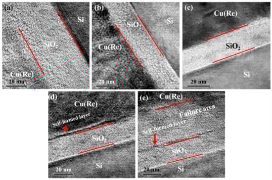
Figure 3.
High-resolution image of the Cu(Re)/SiO2/Si interconnect structure at various temperatures: (a) as-deposited, (b) 350 °C, (c) 450 °C, (d) 550 °C and (e) 650 °C.
Figure 4a,b present the fourteen points, which were perpendicular to the interfaces, selected for the EDX-STEM experiment. The component distribution of the as-deposited sample and Cu(Re)/SiO2/Si sample annealed at 650 °C was assessed using EDX-STEM experiments, as shown in Figure 4c,d. The approximate interfaces of Cu(Re)/SiO2 and SiO2/Si are indicated by black dashed lines in Figure 4c. The component distribution of the O element cannot be measured correctly by the means of the EDX method. Consequently, it is not shown in Figure 4c,d. According to the EDX-STEM depth profiles, as shown in Figure 4c, the as-deposited Cu(Re) film contained about 2.1 at.% Re. The component distribution of the as-deposited sample showed a sharp variation, indicating a distinct interface structure. After annealing, the slopes of the Cu and Si signals in Figure 4d were flatter than those in Figure 4c. This implies that Cu atoms diffused further into the Si substrate in the Cu(Re)/SiO2/Si sample annealed at 650 °C. Figure 4e displays the profile composition of Re for the as-deposited sample and Cu(Re)/SiO2/Si sample annealed at 650 °C. The distribution of Re in the Cu layer in the as-deposited sample maintained a steady value of ~2.1 at.%, and then the value decreased to 0 at.% as it approached the Si substrate. On the contrary, the Re signal was higher in the SiO2 layer in the stack annealed at 650 °C. The above experimental results prove that an obvious enrichment of Re can be detected at the Cu(Re)/SiO2 interface. Thus, the black line as observed in Figure 3d,e was interpreted as the self-formed rhenium-enriched layer. It can be concluded that a minor amount of Re doping plays an indispensable role in the improvement of the barrier properties of pure Cu layers.
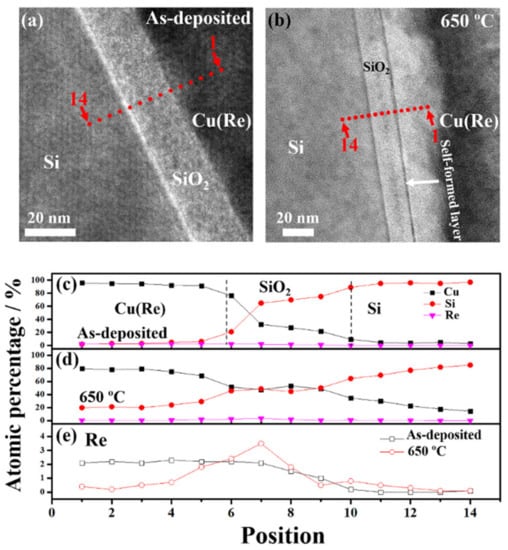
Figure 4.
The positions of STEM-EDX testing of the (a) as-deposited sample and (b) sample annealed at 650 °C. The component distribution of the Cu(Re) film in the (c) as-deposited and (d) 650 °C annealing conditions. (e) The profile composition of Re for the as-deposited sample and Cu(Re)/SiO2/Si sample annealed at 650 °C.
The chemical states of Re at the Cu(Re)/SiO2 interface were analyzed using the XPS method [33,34]. Figure 5 displays the XPS spectra of Re 4f measured at the Cu(Re)/SiO2 interface of the as-deposited film and Cu(Re) film annealed at 650 °C and their fits. For the as-deposited sample in Figure 5a, the peaks at 42.5 and 40.1 eV are characteristic of Re metal, and those at 43.5 and 41.1 eV are characteristic of ReO [35]. This indicates that Re exists at the interface in the chemical form of Re metal and ReO. The fits of the Re 4f photoemission spectra for the sample annealed at 650 °C prove the existence of two additional rhenium oxides in Figure 5b. The doublet at 44.5/42.1 eV was assigned to the Re (IV) oxidation state (ReO2 oxide), and that at higher binding energies 47.7/45.3 eV was assigned to Re (VI) oxidation states (ReO3 oxide) [36]. Specifically, the self-formed layer consisted of Re, ReO2 and ReO3. Generally, ReO3 is known to be very unstable at high temperature and disproportionates to Re 7+ (Re2O7) and Re 4+ (ReO2) upon heating above 400 °C [37,38]. The thermal decomposition is accompanied by the disproportionation reaction [38]
3ReO3→ReO2 + Re2O7
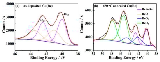
Figure 5.
XPS spectra of Re 4f at the Cu(Re)/SiO2 interface of the (a) as-deposited film and (b) Cu(Re) film annealed at 650 °C.
ReO2 is stable against disproportionation up to 850 °C, while Re2O7 sublimes at a relatively low temperature (reported to be between 225 and 315 °C) [38]. After annealing, only Re metal, ReO2 and ReO3 were observed for the sample annealed at 650 °C. ReO3 should be formed during cooling. Moreover, the Re content of the sample annealed at 650 °C was ~4.3 at.%, which was higher than that of the as-deposited sample (~2.3 at.%). Thus, we consider that the Re alloy diffused to the Cu(Re)/SiO2 interface and reacted with SiO2 to self-form a rhenium-enriched barrier layer during annealing, as observed in the TEM results.
It is well known that the Cu-Re system is essentially immiscible. The solid solubility of Re in Cu is <10−4 at.% [39]. Thus, Re atoms may be driven out from the Cu grains during magnetron sputtering, which would cause Re segregation at the grain boundaries. After annealing, the alloyed Re diffused toward the SiO2/Si interface, which was confirmed by EDX-STEM and XPS testing. Additionally, the formation energy of ReO3 at 400–537 °C was −214.6 KJ/mol, which was less than that of Cu2O at 650 °C (−100.977 KJ/mol) [38,40]. Therefore, Re was more likely to diffuse into the interface and react with SiO2. A self-formed barrier layer was produced which effectively prevented atom interdiffusion.
4. Conclusions
The barrier properties and diffusion behavior of post-annealed Cu(Re) thin films were studied. In summary, a ~2 nm self-formed barrier layer was confirmed by TEM, EDX-STEM and XPS analysis. After doping, Re diffused into the interface of Cu(Re)/SiO2 and reacted with SiO2, which can serve as a barrier layer. The self-formed diffusion layer was found to be composed of Re metal, ReO, ReO2 and ReO3. It can be claimed that excellent thermal stability was observed for the Cu(Re) alloy without a barrier layer after annealing up to 550 °C. The high thermal stability makes the Cu(Re) alloy a promising metallization material for Cu interconnect applications.
Author Contributions
Conceptualization, B.C, Y.Q. and L.W.; methodology, B.C., J.W. (Jun Wang) and Y.Z.; software, H.C.; validation, Y.Z., J.W. (Jun Wang) and F.J.; formal analysis, Z.W. and Y.S.; investigation, B.C., Y.Z. and J.W. (Jun Wang); data curation, Y.Z. and J.W. (Jiheng Wang); writing—original draft preparation, B.C.; writing—review and editing, I.A., Y.Q. and L.W.; supervision, L.J.; fund-ing acquisition, L.W. and L.J. All authors have read and agreed to the published version of the manuscript.
Funding
This work was supported by the Science and Technology Department of Jiangsu Province (BK20130468 and BK 20180984), the National Natural Science Foundation of China (51501074, 82071094, 51905110 and 52005228), the China Postdoctoral Science Foundation (2016M602983), the Jiangsu Overseas Visiting Scholar Program for University Prominent Young & Middle-aged Teachers and Presidents, and the Postdoctoral Science Foundation of Jiangsu (1601047A), Jiangsu Province Medical Key Talents Project (No: ZDRCA2016095).
Institutional Review Board Statement
Not applicable.
Informed Consent Statement
Not applicable.
Data Availability Statement
The data used to support the findings of this study are available from the corresponding author upon request.
Acknowledgments
The authors thank I. Asempah for his valuable help in improving the language of the manuscript.
Conflicts of Interest
The authors declare no conflict of interest.
References
- Wang, F.; Li, D.; Zhang, Z.; Wu, M.; Yan, C. Improvement on interfacial structure and properties of Sn–58Bi/Cu joint using Sn–3.0Ag–0.5Cu solder as barrier. J. Mater. Sci. Mater. Electron. 2017, 28, 19051–19060. [Google Scholar] [CrossRef]
- Wang, L.; Cao, Z.H.; Xu, J.H.; Yu, L.H.; Huang, T.; Meng, X.K. Influence of electric field annealing on atom diffusion in Cu/Ta/Si stacks. Appl. Phys. A-Mater. 2014, 114, 1091–1095. [Google Scholar] [CrossRef]
- Wang, L.; Cao, Z.H.; Syed, J.A.; Hu, K.; She, Q.W.; Meng, X.K. Electric field accelerating interface diffusion in Cu/Ru/TaN/Si stacks during annealing. Electrochem. Solid-State Lett. 2012, 15, H188. [Google Scholar] [CrossRef]
- Wang, L.; Cao, Z.H.; Hu, K.; She, Q.W.; Meng, X.K. Improved diffusion barrier performance of Ru/TaN bilayer by N effusion in TaN underlayer. Mater. Chem. Phys. 2015, 135, 806–809. [Google Scholar] [CrossRef]
- Meng, Y.; Song, Z.X.; Qian, D.; Dai, W.J.; Wang, J.F.; Ma, F.; Li, Y.H.; Xu, K.W. Thermal stability of RuZr alloy thin films as the diffusion barrier in Cu metallization. J. Alloys Compd. 2014, 588, 461–464. [Google Scholar] [CrossRef]
- Chang, S.Y.; Liang, L.P.; Kao, L.C.; Lin, C.F. Electroless- and electroplating of Cu(Re) alloy films for self-forming ultrathin re diffusion barrier. J. Electrochem. Soc. 2015, 162, D96–D101. [Google Scholar] [CrossRef]
- Wang, L.; Asempah, I.; Dong, S.-T.; Yin, P.-P.; Jin, L. Quantitative studies of electric field intensity on atom diffusion of Cu/Ta/Si stacks during annealing. Appl. Surf. Sci. 2017, 399, 215–219. [Google Scholar] [CrossRef]
- Wang, L.; Jin, L.; Yu, L.H.; Dong, S.T.; Chen, J.; Xu, J.H. Evaluation of electric field intensity on atom diffusion of Cu/Ta/Si stacks during annealing. Appl. Phys. A-Mater. 2016, 122, 3. [Google Scholar] [CrossRef]
- Chang, S.-Y.; Li, C.-E.; Chiang, S.-C.; Huang, Y.-C. 4-nm thick multilayer structure of multi-component (AlCrRuTaTiZr)N(x) as robust diffusion barrier for Cu interconnects. J. Alloys Compd. 2012, 515, 4–7. [Google Scholar] [CrossRef]
- Tsai, D.C.; Huang, Y.L.; Lin, S.R.; Jung, D.R.; Chang, S.Y.; Chang, Z.C.; Deng, M.J.; Shieu, F.S. Characteristics of a 10 nm-thick (TiVCr)N multi-component diffusion barrier layer with high diffusion resistance for Cu interconnects. Surf. Coat. Technol. 2011, 205, 5064–5067. [Google Scholar] [CrossRef]
- Liu, B.; Lin, L.W.; Ren, D.; Zhang, Y.P.; Jiao, G.H.; Xu, K.W. Cu(Ge) alloy films with zirconium addition on barrierless Si for excellent property improvement. J. Phys. D Appl. Phys. 2013, 46, 155305. [Google Scholar] [CrossRef]
- Wang, Y.; Tang, B.-H.; Li, F.-Y. The properties of self-formed diffusion barrier layer in Cu(Cr) alloy. Vacuum 2016, 126, 51–54. [Google Scholar] [CrossRef]
- Hsu, K.C.; Perng, D.C.; Wang, Y.C. Robust ultra-thin RuMo alloy film as a seedless Cu diffusion barrier. J. Alloys Compd. 2012, 516, 102–106. [Google Scholar] [CrossRef]
- Wang, Y.; Zhang, M.L.; Cao, F.; Liu, Y.T.; Shao, L. Interficial stability of Cu/Cu(Ru)/Si contact system for barrier-free copper metallization. J. Alloys Compd. 2011, 509, L180–L182. [Google Scholar] [CrossRef]
- Wang, Y.; Yang, X.D.; Song, Z.X.; Liu, Y.T. Property improvement of copper films with zirconium additive for ULSI interconnects. J. Alloys Compd. 2009, 486, 418–422. [Google Scholar] [CrossRef]
- Li, X.N.; Wang, M.; Zhao, L.R.; Bao, C.M.; Chu, J.P.; Dong, C. Thermal stability of barrierless Cu–Ni–Sn films. Appl. Surf. Sci. 2014, 297, 89–94. [Google Scholar] [CrossRef]
- Fang, J.S.; Chen, Y.T. Passivation of copper–hafnium thin films using self-forming hafnium oxide. Surf. Coat. Technol. 2013, 231, 166–170. [Google Scholar] [CrossRef]
- Zhang, X.Y.; Li, X.N.; Nie, L.F.; Chu, J.P.; Wang, Q.; Lin, C.H.; Dong, C. Highly stable carbon-doped Cu films on barrierless Si. Appl. Surf. Sci. 2011, 257, 3636–3640. [Google Scholar] [CrossRef]
- Lozano, J.G.; Lozano-Perez, S.; Bogan, J.; Wang, Y.C.; Brennan, B.; Nellist, P.D.; Hughes, G. Interdiffusion and barrier layer formation in thermally evaporated Mn/Cu heterostructures on SiO2 substrates. Appl. Phys. Lett. 2011, 98, 123112. [Google Scholar] [CrossRef]
- Liu, B.; Song, Z.X.; Li, Y.H.; Xu, K.W. An ultrathin Zr(Ge) alloy film as an exhaustion interlayer combined with Cu(Zr) seed layer for the Cu/porous SiOC:H dielectric integration. Appl. Phys. Lett. 2008, 93, 174108. [Google Scholar] [CrossRef]
- Zheng, Y.H.; Li, X.N.; Cheng, X.T.; Sun, W.; Liu, M.; Liu, Y.B.; Wang, M.; Dong, C. Ni-V(or Cr) Co-addition Cu alloy films with high stability and low resistivity. Mater. Chem. Phys. 2018, 205, 253–260. [Google Scholar] [CrossRef]
- Clearfield, R.; Railsback, J.G.; Pearce, R.C.; Hensley, D.K.; Fowlkes, J.D.; Fuentes-Cabrera, M.; Simpson, M.L.; Rack, P.D.; Melechko, A.V. Reactive solid-state dewetting of Cu–Ni films on silicon. Appl. Phys. Lett. 2010, 97, 253101. [Google Scholar] [CrossRef]
- Chu, J.P.; Lin, C.H. Formation of a reacted layer at the barrierless Cu(WN)∕Si interface. Appl. Phys. Lett. 2005, 87, 211902. [Google Scholar] [CrossRef]
- Wang, Y.; Cao, F.; Zhang, M.L.; Liu, Y.T. Comparative study of Cu-Zr and Cu-Ru alloy films for barrier-free Cu metallization. Thin Solid Films 2011, 519, 3169–3172. [Google Scholar] [CrossRef]
- Lin, P.C.; Chen, H.; Hsieh, H.-C.; Tseng, T.-H.; Lee, H.Y.; Wu, A.T. Co-sputtered Cu(Ti) thin alloy film for formation of Cu diffusion and chip-level bonding. Mater. Chem. Phys. 2018, 211, 17–22. [Google Scholar] [CrossRef]
- Cao, F.; Wang, Y.; Li, F.-Y.; Tang, B.-H. Evaluation of Cu(Ti) and Cu(Zr) alloys in barrier-less Cu metallization. Mater. Chem. Phys. 2018, 217, 412–420. [Google Scholar] [CrossRef]
- Chu, J.; Lin, C.; John, V. Barrier-free Cu metallization with a novel copper seed layer containing various insoluble substances. Vacuum 2008, 83, 668–671. [Google Scholar] [CrossRef]
- Li, X.; Cheng, B.; Asempah, I.; Shi, Q.; Long, A.Q.; Zhu, Y.L.; Wang, Q.; Li, Y.L.; Wang, L.; Jin, L. Effect of Different Ni Contents on Thermal Stability of Cu(Ni) Alloy Film. J. Electron. Mater. 2020, 49, 5674–5680. [Google Scholar] [CrossRef]
- Wang, Y.; Cao, F.; Zhang, M.-L.; Liu, Y.-T. Effects of thermal annealing on Zr-N doped magnetron sputtered copper. Thin Solid Films 2011, 519, 3407–3410. [Google Scholar] [CrossRef]
- Leverant, G.R. Diffusion Barrier for Protective Coatings. U.S. Patent 5,556,713, 17 September 1996. [Google Scholar]
- Nie, L.F.; Li, X.N.; Chu, J.P.; Wang, Q.; Lin, C.H.; Dong, C. High thermal stability and low electrical resistivity carbon-containing Cu film on barrierless Si. Appl. Phys. Lett. 2010, 96, 182105. [Google Scholar] [CrossRef]
- Fei, C.; Gao-hui, W.; Long-tao, J.; Guo-qin, C. Feasibility study on the use of Cu(Co) alloy for barrierless copper metallization. Thin Solid Films 2016, 599, 31–36. [Google Scholar] [CrossRef]
- Qiao, Y.; Wang, X.; Yang, L.; Wang, X.; Chen, J.; Wang, Z.; Zhou, H.; Zou, J.; Wang, F. Effect of aging treatment on microstructure and corrosion behavior of a Fe-18Cr-15Mn-0.66N stainless steel. J. Mater. Sci. Technol. 2022, 107, 197–206. [Google Scholar] [CrossRef]
- Yang, L.; Zhou, Z.; Yang, R.; Wang, J.; Chen, M.; Qiao, Y.; Zhu, S.; Wang, F. Effect of Al and Cr on the oxidation behavior of nanocrystalline coatings at 1050 °C. Corros. Sci. 2022, 200, 110191. [Google Scholar] [CrossRef]
- Morant, C.; Galán, L.; Sanz, J.M. X-ray photoelectron spectroscopic study of the oxidation of polycrystalline rhenium by exposure to O2 and low energy O2+ ions. Anal. Chim. Acta. 1994, 297, 179–186. [Google Scholar] [CrossRef]
- Tysoe, W.T.; Zaera, F.; Somorjai, G.A. An XPS study of the oxidation and reduction of the rhenium-platinum system under atmospheric conditions. Surf. Sci. 1988, 200, 1–14. [Google Scholar] [CrossRef] [Green Version]
- Greiner, M.T.; Rocha, T.C.R.; Johnson, B.; Klyushin, A.; Knop-Gericke, A.; Schlögl, R. The Oxidation of Rhenium and Identification of Rhenium Oxides During Catalytic Partial Oxidation of Ethylene: An In-Situ XPS Study. Z. Für Phys. Chem. 2014, 228, 521–541. [Google Scholar] [CrossRef] [Green Version]
- Shcheglov, P.A.; Drobot, D.V. Heterogeneous equilibria in the rhenium-oxygen system. Russ. J. Phys. Chem. 2006, 80, 1819–1825. [Google Scholar] [CrossRef]
- Shabalin, I.L. Rhenium. In Ultra-High Temperature Materials I; Springer: Manchester, UK, 2014; pp. 317–357. [Google Scholar]
- Holmes, R.D.; Kersting, A.B.; Arculus, R.J. Standard molar Gibbs free energy of formation for Cu2O: High-resolution electrochemical measurements from 900 to 1300 K. J. Chem. Thermodyn. 1989, 21, 351–361. [Google Scholar] [CrossRef] [Green Version]
Publisher’s Note: MDPI stays neutral with regard to jurisdictional claims in published maps and institutional affiliations. |
© 2022 by the authors. Licensee MDPI, Basel, Switzerland. This article is an open access article distributed under the terms and conditions of the Creative Commons Attribution (CC BY) license (https://creativecommons.org/licenses/by/4.0/).