1. Introduction
A favorable combination of the most important physical and mechanical properties of tool ceramics makes it possible to operate ceramic cutting tools at high cutting speeds that are unattainable for tools made of hard alloy. Therefore, ceramic tools can provide a significant increase in machining productivity. In addition, the surface layer quality of parts treated with ceramic tools is noticeably higher. It is worth mentioning that when using ceramic tools, high environmental requirements for machining technologies are ensured, since the cutting is usually performed without toxic cooling lubricants [
1,
2].
Advanced developments in the field of high-quality powders, appearance of new sintering technologies, optimization of their key parameters, and powder compositions provide the production of high-density ceramic blanks with a set of improved properties and allow them to be used for the manufacturing of a wide range of cutting tools, for example, solid ceramic end cutters that have appeared recently on the market [
3,
4]. Improvement in ceramic tools’ shaping processes using diamond tools, the development of surface engineering methods, and bringing the developed technologies to an industrial level have significantly increased their attractiveness for strategically important industries [
5,
6].
A special place among tool ceramics is occupied by materials based on SiAlON, which combines a unique set of physical and mechanical properties (high hardness, strength, and crack resistance), due to which they can be used for cutting difficult-to-machine nickel–chromium alloys, which are indispensable in the manufacturing of aircraft parts on machine tools with computer numerical control CNC [
7,
8]. Ceramics based on SiAlON, which is a mixture of silicon nitride (Si
3N
4) and aluminum oxide (Al
2O
3), has another characteristic feature. This type of ceramic is a dielectric, which imposes certain restrictions on the choice of approaches in the manufacturing cutting tools of this ceramic [
9,
10].
In spite of all these advantages, ceramic cutting tools’ share of industrial use in the total global market for machining tools is low and does not show significant growth. According to expert estimates, the current share of ceramic tools in the world market of bladed tools is 10–11% [
11,
12]. This is a direct consequence of the insufficient operational stability of the ceramic tools. Under the influence of increased thermal and power loads, sudden microdestruction of the cutting part often occurs [
13,
14]. The use of systems for monitoring and diagnosing the state of a cutting tool in real time, effective when cutting with carbide tools, is ineffective when machining with ceramic tools, since a significant part of the failures occurs suddenly. It should be taken into account that when machining nickel–chromium alloys, the level of thermal and power operational loads on the cutting part of a ceramic tool is especially high and the risk of sudden microfracture increases [
15].
The technological approaches to the manufacturing of ceramic tools used in the tool industry do not provide “defect-free” products. After final processing, their surface layer is replete with defects, which are formed in the process of diamond sharpening.
Figure 1 shows the SEM images of a commercially available tool made of SiAlON ceramic after diamond sharpening, where characteristic defects on the working surface and the cutting edge are clearly visible. The surface after diamond grinding has an uneven relief. Shallow scratches are clearly visible, alternating with deep grooves profiled with single diamond grains, tearing of grain particles, and conglomerates of grains under the action of cutting force and other defects, which are described in detail by various research groups [
16,
17]. When, during cutting, the operating loads act on the ceramics surface layer with pronounced defects, it is extremely difficult to predict the destruction mechanism of the tool cutting part [
18,
19].
The circumstances described above largely explain the rather modest effect that is observed when applying wear-resistant coatings TiAlN, CrAlN, TiZrN, TiCN, DLC, etc. on the working surfaces of ceramic tools and their application under conditions close to operational ones [
20,
21]. At the same time, the application of similar nitride and diamond-like coatings to a hard alloy tool due to an increase in microhardness, a decrease in frictional, and adhesive interaction on the contact pads makes it possible to ensure high operational stability and increase wear resistance by an average of three times, even when machining hard-to-machine titanium and nickel alloys [
22,
23].
For ceramic tools, the maximum achieved effect is about 1.6–1.8 times for oxide–carbide ceramics when machining structural and hardened bearing steels. At the same time, the operational stability of the ceramic tool (the spread of cutting time before failure) remains significant [
24,
25]. For processing of nickel–chromium alloys with SiAlON ceramics, there are isolated studies where attempts have been made to increase the wear resistance of contact pads by forming coatings [
26,
27]. In particular, with the participation of the authors of this work, it was possible to increase the wear resistance of ceramic end mills up to 1.5 times due to the pretreatment and deposition of a multilayer (CrAlSi)N/DLC coating.
It is obvious that the impossibility to fully realize the potential of wear-resistant coatings deposited on tool ceramics is mainly due to the defective state of the surface, which occurs after diamond sharpening. High efficiency cannot be expected from a thin coating deposited on a defective layer. Previously, experts in the field of tool ceramics believed that the coating is able to “heal” surface defects by filling them [
28,
29]. Practice shows that a coating with a thickness not exceeding 4 microns (a coating of greater thickness peels off from ceramic substrates) can only partially level out surface defects. It is able to fill small scratches or chipped particles of grains, but does not allow leveling deep grooves and filling voids from torn grains [
30,
31].
The only solution to eliminate or minimize the presence of a defective layer is pretreatment before coating. Precision finishing or polishing could solve this problem and create a favorable basis for the subsequent formation of coatings [
32,
33]. At the same time, it is necessary to take into account the economic factor—replaceable ceramic inserts are high-wear consumables of mass production with a short service life. Therefore, to ensure the profitability of their production, possible additional processing before coating should not increase the cost of the tool manufacturing cycle.
When developing technological principles, it is necessary to proceed from a set of requirements related to ensuring high process productivity when processing a wide range of tool ceramics (including dielectrics), high uniformity of tool working surfaces, and the absence of additional damaging effects on the surface layer of samples, distortion of microgeometry, and a significant deterioration in the roughness of the tool, as well as the possibility of combining the process of removing a defective layer into one finishing technological operation with the process of wear-resistant coatings deposition. For the controlled removal of a thin defective layer formed during abrasive processing from a ceramic tool surface, sputtering by accelerated ions or fast neutral atoms can be used. In the same vacuum chamber, it can be combined with subsequent coating deposition using a magnetron sputtering system, which is often used for deposition of thin coatings on dielectric substrates [
34,
35].
When using magnetron sputtering systems, the coating properties depend on the energy supplied to the atoms condensing on its surface. This energy can be transferred through the substrate heating [
36]. In addition, it can be transported by accelerated ions [
37]. In such cases, a non-equilibrium atomic scale heating of the coating and substrate, which is independent of the substrate temperature, replaces the equilibrium heating. This allows coating deposition on heat-sensitive materials.
The coating properties depend not only on the energy of accelerated ions, but also on the ratio of the flow density of condensing atoms to that of accelerated ions impinging the coating [
38,
39]. Increase in the ion energy up to 5–10 keV can result in sputtering of all deposited atoms. Therefore, for coating modification with high-energy ions, pulsed regimes are used. Due to mixing of the substrate and coating materials by ions [
40], the interface width can reach 5 μm [
41,
42]. This ensures a perfect adhesion of hard coatings with a thickness of 10–50 μm. The pulsed impingement by high-energy ions allows nc-Ti
2N/nc-TiN nanocomposite coatings with microhardness of 5000 HV0.04.
Conductive substrates immersed in plasma can be processed with accelerated ions by means of application of a negative pulsed [
41,
42] or DC [
43,
44] bias voltage. As for the magnetron discharge plasma, it is free of metal micro particles, which are typical of the arc discharge plasma [
45,
46]. However, the magnetron sputtering is characterized by a comparatively low plasma density near the substrate surface [
47] and low ionization degree of sputtered atoms. The ionization degree of sputtered atoms increased to 60–80% when high-power pulsed magnetrons were used [
48,
49]. The plasma density near the negatively biased substrate increased many times when unbalanced magnetrons [
50,
51] were introduced.
Negative bias voltage cannot be applied to dielectric substrates. Any dielectric substrate immersed in plasma is impinged with ions accelerated by a floating potential of 10–30 V. However, when a flat dielectric sample is placed on a flat conductive holder connected to an RF power supply, the voltage accelerating the ions can increase to hundreds of volts [
52]. These ions can sputter the flat dielectric sample quite uniformly. Nevertheless, the expensive and unhealthy RF technique cannot allow a uniform etching of complex-shaped dielectric parts [
53]. To regulate properties of any coatings on dielectric parts, broad beams of accelerated ions [
54,
55] or fast gas atoms [
56,
57,
58] can be used. There are some beam sources of fast gas atoms that accompany the slow metal atoms [
59] on their way from a common emissive grid to the substrate surface.
The charge accumulation in the volume and on the surface of a non-conductive substrate being processed with an ion beam results in strong electric fields deviating the ion trajectories. This leads to inhomogeneous etching of the substrate surface. The etching rate of any material by fast neutral atoms is equal to the rate of etching by their ions with an equal kinetic energy. Therefore, the dielectric parts should be preferably processed with beams of fast neutral atoms.
When fast gas atoms are produced due to charge exchange collisions of accelerated ions with gas molecules on their way from the emissive grid of a beam source to a dielectric substrate, the number of residual ions in the beam decreases exponentially. Neglecting the gas heating in the discharge, we suppose that at
p = 0.1 Pa density of the gas molecules
no = 2.5 × 10
19 m
−3 [
60]. When the energy of argon ions increases from 0.5 up to 6 keV, their charge exchange cross-section σ
c decreases from 3 × 10
−19 to 1.7 × 10
−19 m
2 [
61,
62] and their charge exchange length λ
c = 1/
noσ
c increases from 0.13 to 0.24 m. Hence, any beam produced due to charge exchange collisions includes the residual ions. Fast atoms can appear due to interactions of ions with metal surfaces [
63] and can provide removal of ions from the beam.
The main aim of this research was to increase the wear resistance of round cutting plates manufactured using SiAlON dielectric ceramics by means of wear-resistant coating deposition. To reach this goal, the coatings’ adhesion had to be improved due to removal of a defected surface layer by a beam of fast argon atoms prior to the deposition. Wear-resistant TiAlN coatings deposited after the etching were found to significantly improve the processing stability and increase wear resistance of the cutting plates.
2. Materials and Methods
2.1. Materials
The tool material used in this study was AS500 (TaeguTec, Daegu, Korea) commercial silicon nitride-based ceramic, which has improved chipping resistance and hardness required for cutting difficult-to-machine nickel alloys. The specified tool ceramics has the following physical and mechanical characteristics: density–3.21 g/cm
3, HRA hardness–94.3, flexural strength–850 MPa [
64].
In the experiments, samples of the RNGN type ceramic cutting inserts, round in shape without a hole with a diameter of 19.05 mm and a height of 7.9 mm (
Figure 2a), were used. During the performance tests, a cutting plate was installed in a tool holder and rigidly fastened with a clamp from above (
Figure 2b).
Structural-phase analysis of AS500 ceramics shows that this material is a classical SiAlON microstructure, which is a combination of elongated grains, as well as unequal and equiaxed polyhedral grains (
Figure 3a). X-ray phase analysis on a Bruker D8 Advance (Bruker AXS, Karlsruhe, Germany) diffractometer under conditions of monochromatic Cu Kα radiation made it possible to reveal the following three main phases in a tool ceramic sample: Si
5AlON
7, Si
3N
4, and Al
2O
3 (
Figure 3b).
Operational tests were carried out under laboratory conditions on a universal lathe CU 500 M manufactured by ZMM Sliven (Bulgaria) with a stepless spindle speed control. The experiments were carried out under the following cutting conditions: speed V = 200 m/min, feed S = 0.1 mm/rev, and depth t = 0.5 mm (without coolant).
As a criterion for the wear of the ceramic plate during operation, wear along the back surface was taken, the limit value of which is 0.4 mm. When this value is reached during turning, the tool retains its operable state, and exceeding this value quickly leads to the development of catastrophic wear. The amount of wear of the ceramic plate on the flank was monitored after every two minutes of operation. In order to evaluate the stability of the performance of ceramic plates, each experiment was duplicated eight times. Wear was measured using a SteREO DiscoveryV8 metallographic microscope manufactured by Carl Zeiss Microscopy (Jena, Germany).
A bar made of heat-resistant alloy XH45MBTJuBP (analog of Inconel 718) was used as the material to be machined. According to the data presented by the producer of this material (Industrial Metallurgy, Ltd., Moscow, Russia), it has the following physical and mechanical characteristics: HB hardness—320 units, elastic modulus—210 kN/mm
2, density—8.2 g/cm
3, tensile strength—1080 MPa.
Table 1 provides information on the chemical composition evaluated using our X-ray fluorescence spectrometer Bruker S8 TIGER Series 2 (Bruker AXS, Karlsruhe, Germany).
2.2. Methods for Processing of Cutting Plates
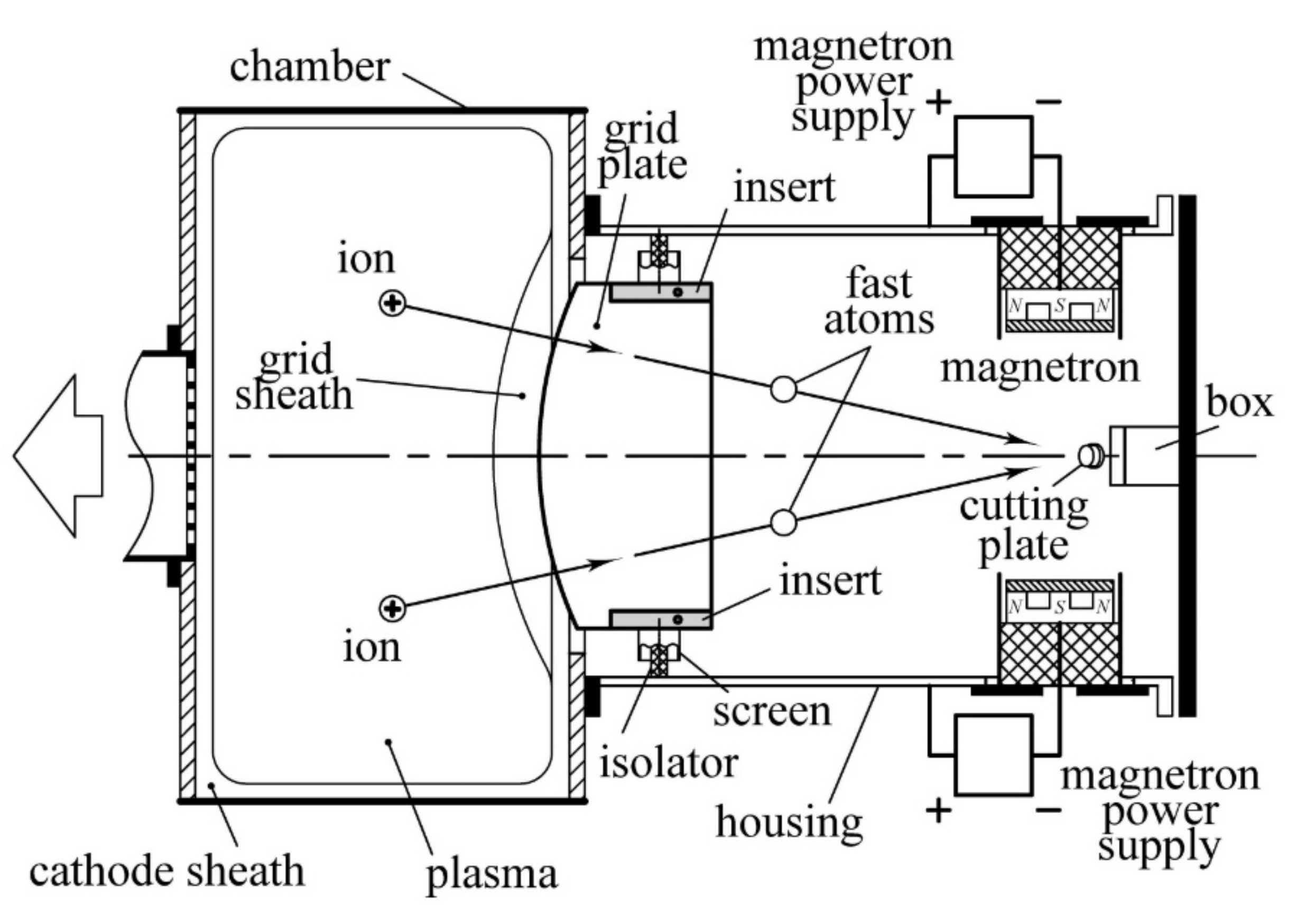
The experimental system used for processing of cutting plates made of SiAlON is presented in
Figure 4. It comprises a 50 cm-diameter and 30 cm-long vacuum chamber evacuated through a flat grid to a pressure of 0.001 Pa by a rotary pump and a turbo-molecular pump (not shown in
Figure 4). The grid prevents the plasma penetration into the pumping system. On the right wall of the chamber is mounted a 30 cm-high, 40 cm-wide, and 50 cm-long rectangular housing with a removable flange. There is a rectangular 22 cm-high and 32 cm-wide opening in the chamber wall between the chamber and the housing. A grid composed of 20 parallel 150 mm-long, 300 mm-wide, and 0.5 mm-thick titanium plates is placed inside the housing. The plates are fastened together using 4.5 mm-thick inserts between and tightening studs. Using four ceramic isolators protected from deposition of metallic films with hollow cylindrical screens, the grid is fastened to the housing walls. Facing the vacuum chamber, sections of plane-parallel plates of the grid are shaped as segments of a 50-cm radius (
Figure 5). Through the opening of the chamber wall, the grid is inserted into the chamber by 2 cm. It is connected through a high-voltage feedthrough mounted on the top of the housing to an accelerating voltage power supply. This power supply allows regulation of the negative bias voltage on the grid from zero to 5 kV.
On the removable flange of the housing is mounted a substrate rotation system (
Figure 4). Seven 18 mm-diameter cutting plates made of SiAlON are fastened thereon in a vertical line. Each plate is placed on its individual holder fastened to one of the eight parallel axes connected to each other with gears. The angle of the axes relative to the flange is 45 degrees. When the first upper plate is rotated clockwise, the second adjacent plate is rotating counterclockwise. Accordingly, the third, fifth, and seventh cutting plates rotate clockwise, and the fourth and sixth plates rotate counterclockwise. The rotating axes with transmission gears are mounted in a closed box protecting them from film deposition.
Two planar magnetrons are mounted on both sidewalls of the housing near the substrate rotation system. The magnetron targets’ width is equal to 100 mm. Their length of 250 mm exceeds the length of the cutting plates array amounting to 150 mm. One of the targets is made of titanium and the other of aluminum. The magnetron targets are distant from the cutting plates at ~100 mm.
There is a quartz window on the top of the housing. It allows remote measurements of the substrate temperature with an infrared pyrometer IMPAC IP 140 manufactured by LumaSense Technologies GmbH (Frankfurt am Main, Germany).
The working gases (argon and nitrogen) are admitted to the housing from a two-channel gas supply system. Through the gaps between the plates of the grid, they pass into the vacuum chamber and are evacuated through the pumping system. The gas pressure in the chamber is measured with a vacuum gauge Baratron and regulated with a control panel. From the same panel, the currents of magnetron power supplies, the gas discharge power supply between the chamber and the anode, and the accelerating voltage power supply between the grid and the chamber are controlled.
At a gas pressure of 0.5 Pa, turning on the discharge power supply leads to gas breakdown between the vacuum chamber and the anode. As a result, the chamber is filled with a homogeneous plasma of glow discharge with voltage of
U ~ 400 V. The chamber plays the role of a hollow cathode with volume of
V = 0.059 m
3 and inner surface area of
S = 0.86 m
2. The cathode surface is separated from the plasma with a sheath of positive space charge. The sheath width
d depends on the voltage
U and the ion current density
j from the plasma to the cathode. According to the Child–Langmuir law [
65]:
where ε
o is electrical constant,
e is the electron charge, and
M is the ion mass. While measuring
M =
AMo in atomic mass units
A = 1.66 × 10
−27 kg:
Taking into account that argon ion mass is equal to
Mo = 40, the mean width of the sheath
d is equal to 5 mm at the ion current density
j = 2.76 A/m
2 and the ion current of
Ii =
jS = 2.76 × 0.86 = 2.37 A. When the ion energy does not exceed 0.5 kV, the coefficient of secondary ion–electron emission is equal to γ ≈ 0.05 [
66] and the ion current is close to the discharge current
I. Hence, at the discharge current
I not exceeding 2 A, the sheath width exceeds the width of the gaps between the grid plates amounting to 4.5 mm.
Electrons accelerated in the cathode sheath pass through the plasma and in the opposite sheath are repelled back to the plasma. They can pass through the plasma up to hundred times and the length of their way from the chamber wall to the anode L = 4V/Sa, where Sa is the anode surface can exceed the width of the chamber by two orders of magnitude. At a constant current, for instance I = 2 A, the discharge voltage U is independent of the gas pressure p until it diminishes to a value po, at which the passage of emitted gas by the chamber electrons Λ needed to spend all their energy eU on gas ionization grows to L. Each of them produces N = eU/W ions, where W is the ionization cost of the gas; argon W = 26 eV. A comparable contribution to the gas ionization produces fast electrons in the cathode sheath of the discharge.
At the anode surface area Sa = 45 cm2, the discharge voltage U between the anode and the chamber does not practically change with argon pressure decreasing to po ~ 0.1 Pa. However, with a further decrease in pressure, it grows to U ~ 1 kV at p = 0.02 Pa, because at Λ > L, electrons spend on ionization only a part of their energy. However, the discharge current is maintained due to the growing contribution of fast electrons from the cathode sheath, whose number increases with the discharge voltage and cathode sheath width.
Application to the grid of accelerating voltage
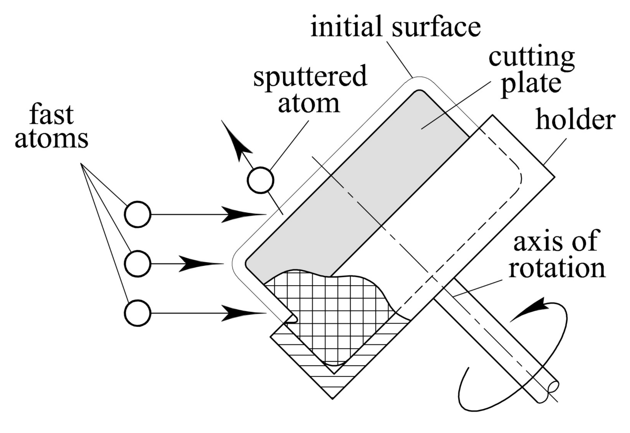
Ua appreciably increases the width of the sheath between the grid and plasma. Ions from the plasma are accelerated in the sheath and enter the gaps between the grid plates. Due to the inhomogeneity of the electric field at the ends of the grid plates, the ions are scattered at small angles. Therefore, they touch the plates and turn into fast atoms. As sections of the grid plates facing towards the vacuum chamber are shaped as segments of a 50 cm-radius circle, trajectories of the fast atoms are directed to the center of this circle (
Figure 5). Therefore, the width of the fast atom beam decreases from 30 cm near the grid sheath to 2.5 cm near the rotating cutting plates. The flux density of fast argon atoms and the rate of cutting plates etching increase in this case by a factor of 30/2.5 = 12.
Taking into account increase in the flux density by 12 times, power density transported by the fast atoms to a cutting plate at the current density
j = 2.76 A/m
2 of ions with energy of 400 eV, which enter the grid with transparency of 0.9, can be assessed as
w = 2.76 × 400 × 0.9 × 12 = 11,923 W/m
2. The surface power density of the plate thermal radiation is determined by its temperature
T:
where σ
S-B = 5.7 × 10
−8 W/(m
2 K
4) is the Stefan–Boltzmann constant, α~0.6 is the plate emissivity, and its temperature
T is measured in kelvin (K). In a state of equilibrium, the power of the thermal radiation
R*
Ssub of the cutting plate, where
Ssub is its surface area, is approximately equal to the power
wSsubη of fast atoms heating the substrate, where η~0.2 is the surface part being impinged by fast atoms. Hence, the substrate temperature is equal to
T = (η
w/ασ
S-B)
1/4 ≈ 514 K ≈ 240 °C, which is enough for heating and etching dielectric substrates before coating deposition.
When accelerating voltage applied to the grid increases to 4 kV, the etching rate grows by an order of magnitude. At the equal angles of incidence to the front and back surfaces of the cutter amounts to 45 degrees, two-hour-long etching of cutting plates can provide removal from the surfaces of defective layers with a thickness up to 10 μm (
Figure 6). As the depth of grooves that occur after diamond grinding of the plates does not exceed 10 μm, the etching can level out the surface defects.
Preliminary tests revealed that (presented in
Figure 5) magnetron at the current of 4 A in the titanium target circuit ensures a TiN coating deposition rate of 2 μm/h on a substrate distant from the target at 100 mm. The use of two magnetrons with titanium and aluminum targets in simultaneous operation can provide deposition on a SiAlON cutting plate of 3 μm-thick TiAlN coating just after removal of the defective layer from its surface.
2.3. Instruments for Characterisation of the Plates
An optical 3D measuring system MicroCAD Premium plus manufactured by GFMesstechnik GmbH (Berlin, Germany) was used to measure the cutting edge radius of the plate.
A stylus profiler Dektak XT manufactured by Bruker Nano, Inc. (Billerica, MA, USA) was used to measure the surface roughness, coating thickness, and thickness of the removed surface layer.
An infrared pyrometer IMPAC IP 140 manufactured by LumaSense Technologies GmbH (Frankfurt am Main, Germany) was used to measure the cutting plate temperature.
Nanovea M1 Hardness and Scratch Tester produced by Nanovea Mechanical Testing (Irvine, CA, USA) was used to measure the coating microhardness and adhesion.
A Calotest instrument produced by CSM Instruments (Peseux, Switzerland) was used to evaluate the abrasion resistance of the plates.
A VEGA-3LMH scanning electron microscope manufactured by TESCAN (Brno, Czech Republic) was used for obtaining images of the plate surface.
A SteREO DiscoveryV8 metallographic microscope manufactured by Carl Zeiss Microscopy (Jena, Germany) was used to measure the cutting plate wear.
3. Results and Discussion
3.1. Etching of The Cutting Plates
In order to evaluate the etching rate of cutting plates by fast argon atoms, five plates were in turn placed on the central rotating holder (
Figure 4) and for one hour processed at gas pressure
p = 0.1 Pa, discharge current
I = 2 A, and various accelerating voltages
Ua. During the etching, the cutting plate temperature was simultaneously measured.
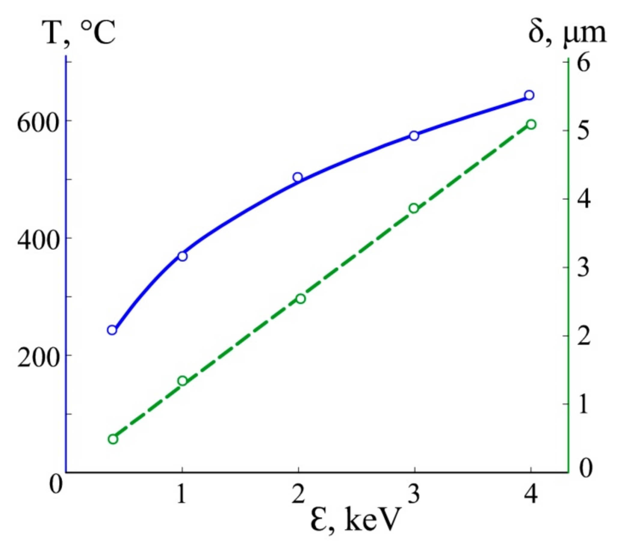
Figure 7 presents the dependencies of the cutting plate temperature
T and thickness δ of the defective layer removed per one hour from the plate surface by fast argon atoms on their energy ε =
e(
U +
Ua).
To evaluate the layer thickness, a profilogram of its cylindrical surface was obtained and height of the step between the parts of the profilogram corresponding to the plate surface screened with the holder and its open surface was measured. The step height is exactly equal to the removed layer thickness.
Figure 7 shows that the sputtering rate is directly proportional to the energy ε of fast atoms and at ε = 4 keV amounts to ~5 μm/h. Temperature of the cutting plate grows from 240 °C at ε = 0.4 keV to 640 °C at ε = 4 keV. It is worth noting that the sputtering coefficient for SiAlON is much lower than that for single-element solids [
67].
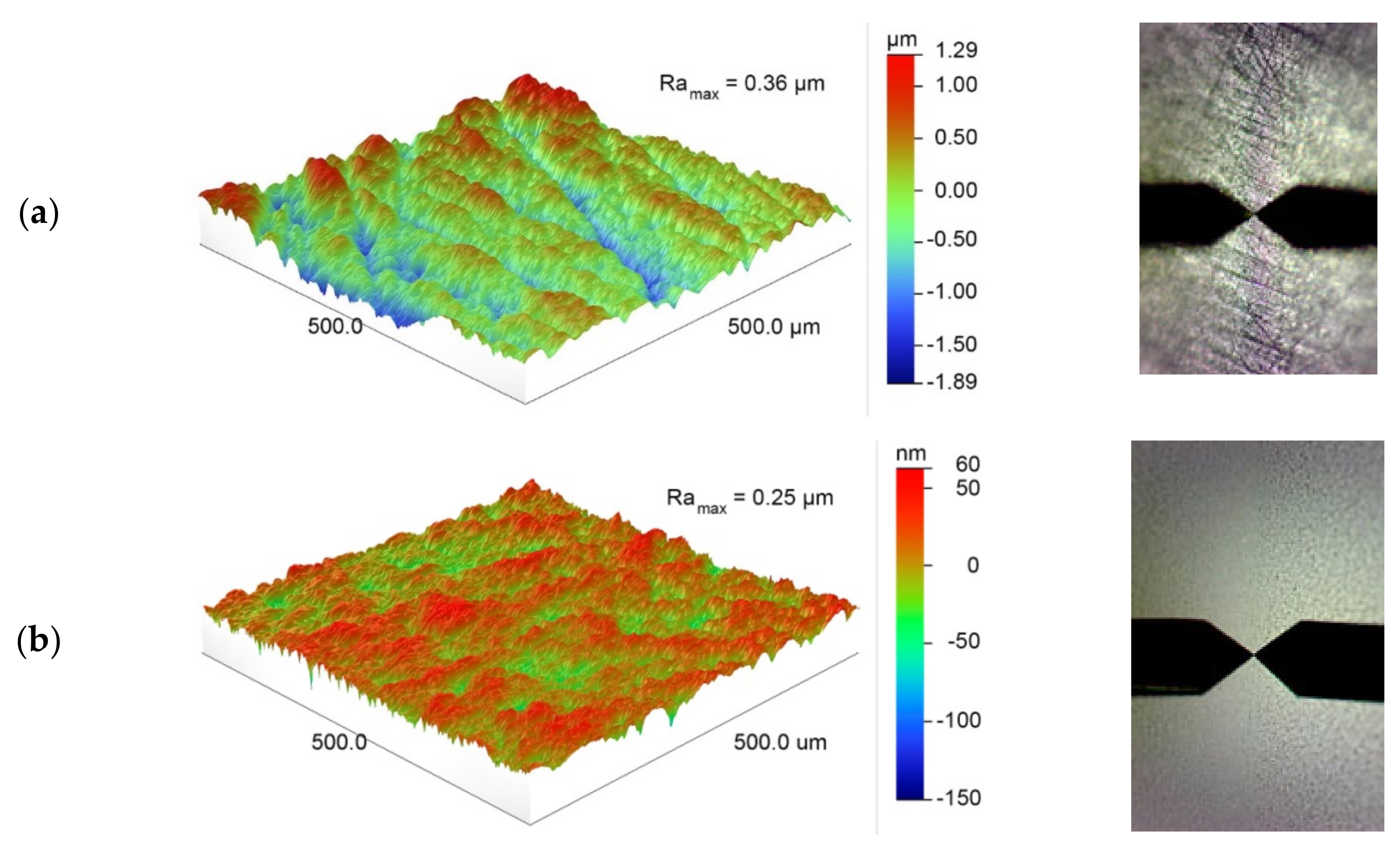
Figure 8 presents SEM images of a cutting plate surface before (a) and after processing with fast argon atoms (b). The initial surface is replete with defects, formed in the process of diamond grinding scratches and microscopic caverns. There were no such defects after a two-hour-long etching of the surface by 4 keV argon atoms under an angle of incidence of 45° and removal of a 10 μm thick surface layer.
Figure 9 presents, using a stylus profiler Dektak XT, profilograms of a cutting plate surface before (a) and after (b) removal of a 10 μm-thick layer from its surface (on the left) and photographs of the plate surface and a stylus with its shadow on the surface (on the right). It can be seen that before processing, the surface is replete with numerous microscopic scratches and the scratches’ depth reaches 3 μm. Etching the rotating cutting plate by fast argon atoms at their angle of incidence to the plate surface of 45 degrees made it possible to appreciably level out the surface defects. After removal of a 10 μm-thick layer from the plate surface, no scratches were seen and the surface roughness decreased to R
a = 0.25 μm.
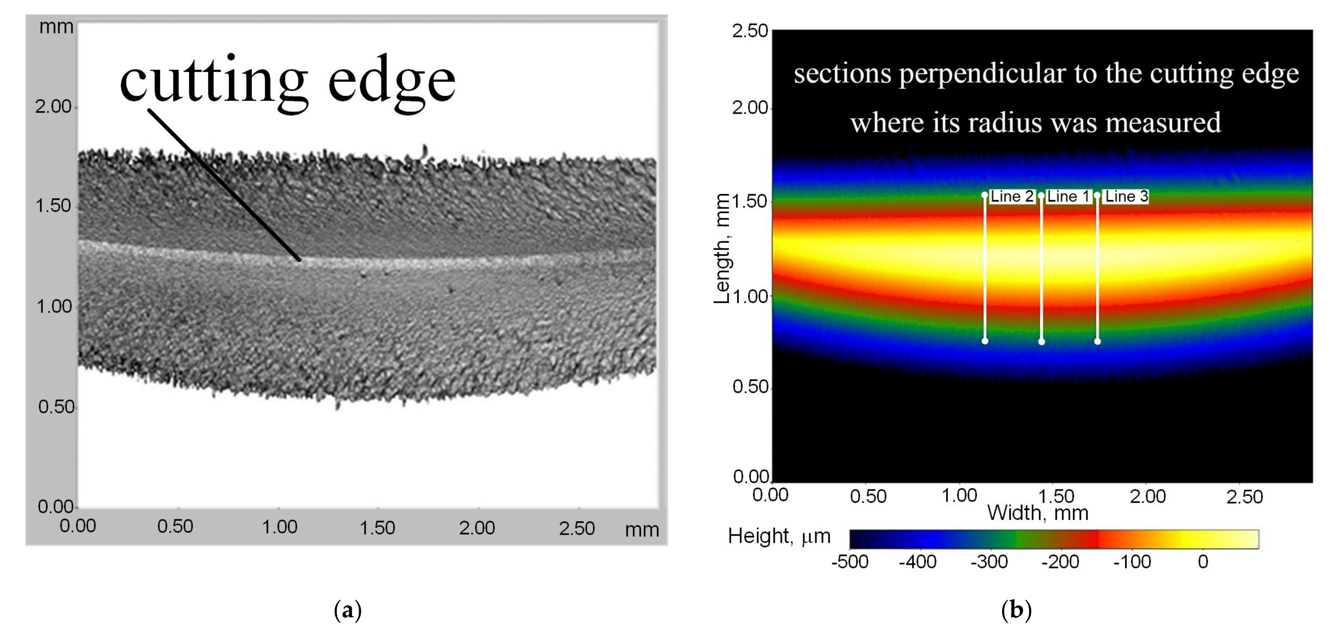
The influence of the fast argon atoms on the cutting edge radius of the plate (
Figure 10) was evaluated by measuring before and after processing using an optical 3D measuring system—MicroCAD Premium plus manufactured by GFMesstechnik GmbH (Germany). The device is a metrological system that uses light band projection profilometry to create three-dimensional models of the scanned surface. These three-dimensional models serve to measure their dimensions. Vertical lines in
Figure 10 indicate three sections distanced from each other at 0.3 mm, where the cutting edge radius was measured.
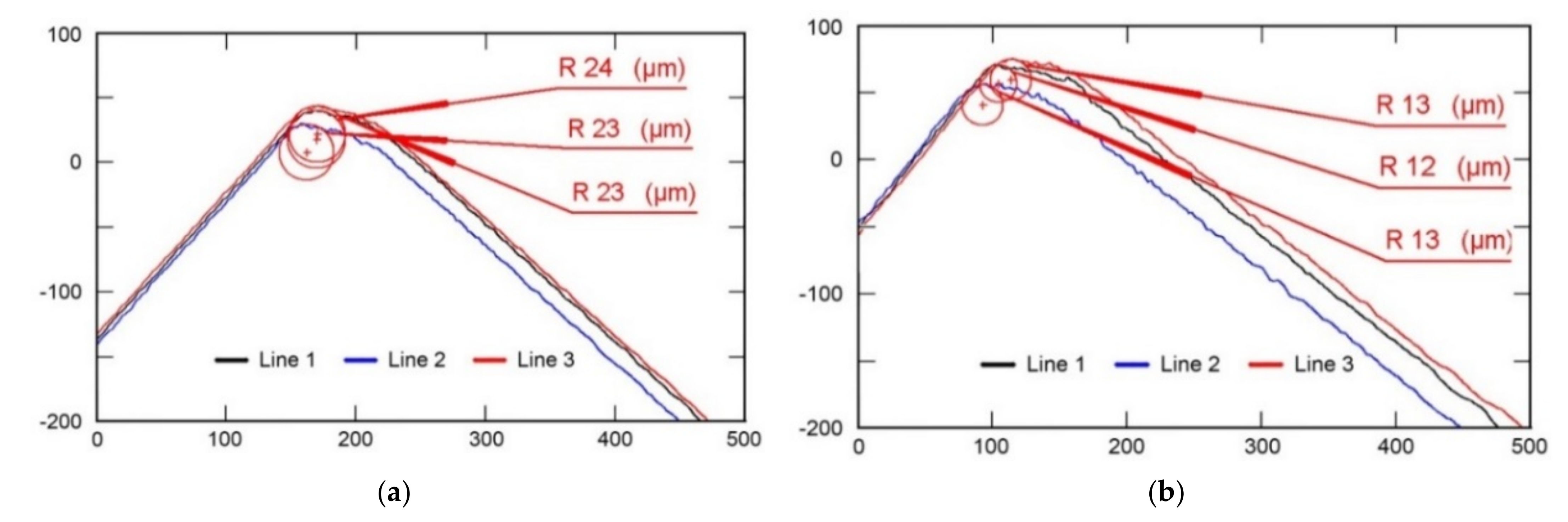
Figure 11a presents a 3D image of the cutting wedge surface and a circle inscribed in the wedge top. The MicroCAD (version Premium plus) system makes it possible to obtain profiles of the surface in any cross-section and to measure the radius of the inscribed circle, which is equal to the cutting edge radius. The value of the radius is found as the arithmetic mean of the values measured for three sections. For the initial cutting plate, it amounts to R = 20.3 μm. After a two-hour-long etching of the cutting plate by 4-keV argon atoms, the cutting edge radius diminished by about two times to R = 9.7 μm.
3.2. Coating Deposition
One of the cutting plates was placed on a central rotating holder (
Figure 4) and processed by fast argon atoms with energy of ε = 1 keV at gas pressure
p = 0.1 Pa and discharge current
I = 2 A. In 10 min, the plate temperature increased to 370 °C, 30% addition of nitrogen was admitted to argon, and two planar magnetrons with titanium and aluminum targets were turned on. During the synthesis on the plate surface of TiAlN coating at currents in the circuits of the magnetron targets of 4 A, it was continuously bombarded by fast argon and nitrogen atoms with energy of 0.4 keV. After a 30 min-long deposition, the cutting plate was withdrawn out of the holder and a profilogram of its cylindrical surface was obtained. The height of the step between the parts of the profilogram corresponding to the plate surface screened with the holder and open surface coated with TiAlN was measured. The coating thickness is equal to the step height of ~3 μm.
Figure 12 presents SEM images of cutting plates surfaces coated before processing with fast argon atoms (a) and after the processing (b).
In the first case, microscopic caverns are seen in spite of the deposited coating. There are no such caverns on the plate coated after removal of the 10 μm-thick surface layer by 4-keV argon atoms.
Cutting edge radii of coated plates were measured in three sections distanced from each other at 0.3 mm. The measurement results are presented in
Figure 13. The value of the cutting edge radius is found as the arithmetic mean of the values measured for three sections. It amounts to 23.3 μm for the plate not etched by fast argon atoms and to 12.7 μm for the plate coated after removal of a 10 μm-thick defective surface layer by fast argon atoms.
3.3. Abrasion Resistance and Wear of Cutting Plates
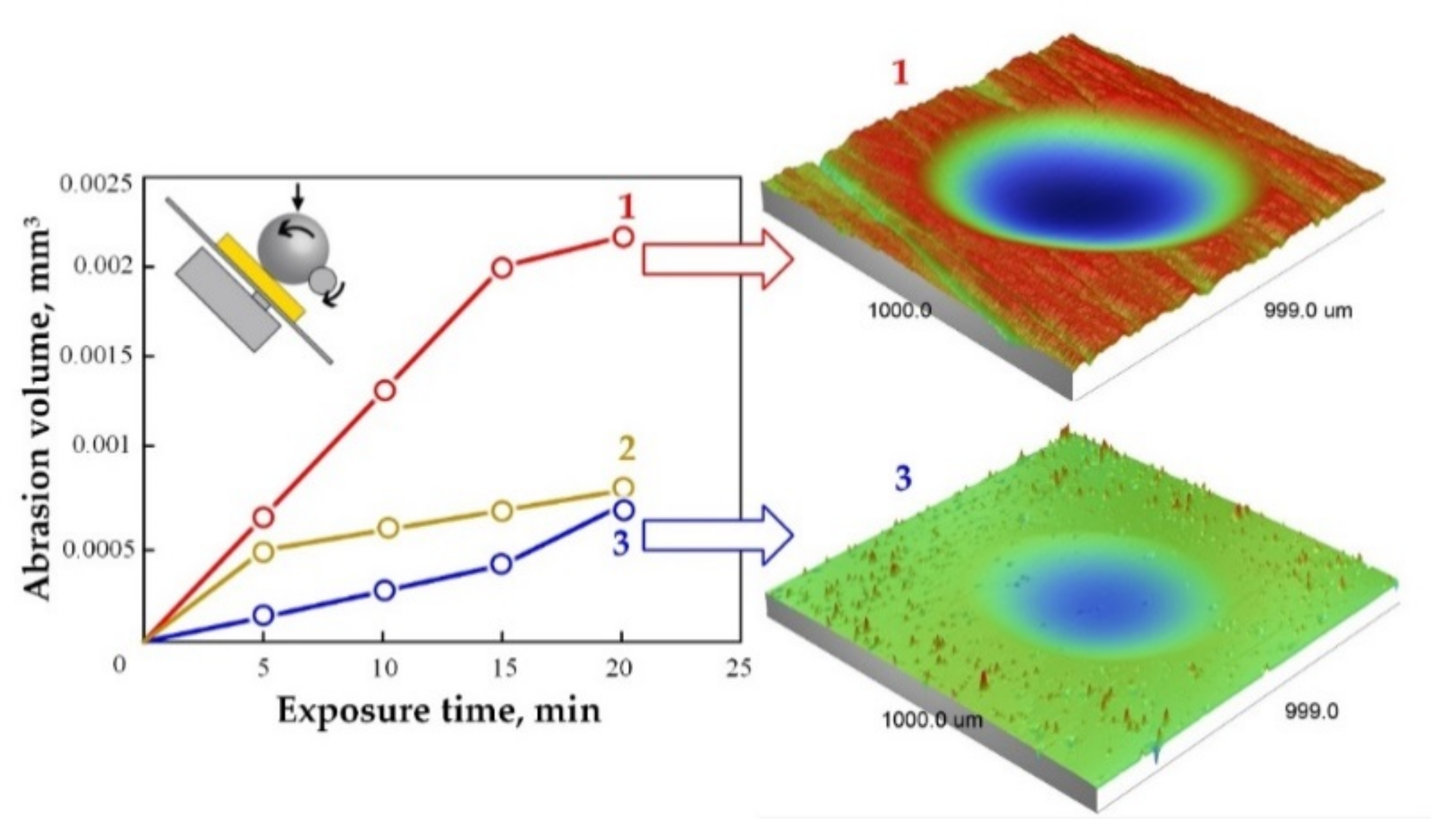
To evaluate the abrasion resistance of the SiAlON cutting plates and their dependence on processing with fast argon atoms and deposition of wear-resistant coatings, a Calotest instrument produced by CSM Instruments (Peseux, Switzerland) was used. A rotating ball was placed on the cutting plate with a load of 0.2 N and an abrasive suspension was fed into the contact zone. Abrasive particles in the contact zone and an applied external force led to local abrasion of the plate surface. As the ball rotates, it produces a spherical wear notch on the plate surface. The diameter
D of the notch is determined using an optical microscope. When the ball radius R appreciably exceeds
D, the volume of worn material is equal to V = π∙d
4/64R.
Figure 14 presents dependencies of the abrasion volume on the test time for a not-processed cutting plate (1), a plate with TiAlN coating (2), and a plate coated with TiAlN after removal of the 10 μm-thick defective layer from its surface (3). This shows that due to the defective layer removal and deposition of wear-resistant coating, the abrasive wear diminished by an order of magnitude.
For characterization of the coating adhesion, a Hardness and Scratch Tester produced by Nanovea Mechanical Testing (Irvine, CA, USA) was used. The coating microhardness was equal to 2100 HV40. The first critical load resulting in appearance of an acoustic emission and first cracks on the coating amounted to Lc1 = 12 N for the plate coated without removal of its surface layer. It amounted to Lc1 = 28 N for the plate coated with TiAlN after removal of a 10 μm-thick defective layer from its surface by argon atoms with energy of 4 keV. The adhesion improvement is the result of surface activation by the fast atoms.
Comparative laboratory operational tests of round SiAlON ceramic plates during the turning of a nickel–chromium alloy (
Figure 15) reveal significant differences, both in the nature of the development of wear curves over time and in the intensity of wear growth along the flank surface for plates that have undergone various types of surface treatment. Ceramic plates without coating (1) and with TiAlN coating (2) exhibit characteristic wear stages “running in–steady wear–catastrophic wear” (for plates with TiAlN, the last stage is less pronounced).
At the running-in stage, during the first two minutes of operation, the size of the wear area on the flank increases markedly, reaching an average value of 0.27 mm for an uncoated tool and 0.18 mm for a tool coated with TiAlN. This can be explained by the imperfection of the surface layer formed during sharpening. It is known from the theory of friction that rougher mating surfaces are more difficult to run in and the coefficient of friction during running in and, accordingly, the wear rate, is much higher than that for better prepared surfaces [
68,
69]. Obviously, when a defective surface layer of a ceramic plate comes into operation and in contact with the workpiece being processed, high thermal and mechanical loads act on it; thus, the initial stage of operation is accompanied by the destruction of existing irregularities and discontinuities.
The end of running-in and the stage of steady-state wear occurs only after stabilization of the conditions of contact interaction between the surfaces and the friction process. For plates with TiAlN, compared to plates without coating, the surface is characterized by a somewhat lower defectiveness, which, together with a higher microhardness of the contact pads, provides a smaller size of the wear pad at the running-in stage. Attention is drawn to the fact that for beam-finished ceramic samples with a TiAlN coating (3), which have a minimum number of defects, no pronounced running-in stage is observed, and the average size of the wear area during the first two minutes of operation is no more than 0.06 mm.
Subsequently, for uncoated plates, a monotonous increase in the wear area on the back surface is observed for about 5–6 min, after which a rather sharp transition to the stage of catastrophic wear follows. Such a relatively short stage of steady wear for sample (1) in comparison with the plates with coatings (2) and (3) should be explained by the so-called “boundary effect”. In the process of cutting, the contact of the tool with the workpiece occurs along the wear chamfer on the back surface, and the intensity of its development in time depends not only on the properties of the tool material directly in the contact area, but also largely on the characteristics of the surface layer along the contact boundaries.
The coating at the contact boundaries can reduce the intensity of wear chamfer development and provide a more monotonous wear pattern without a sharp transition to the catastrophic stage, which is clearly demonstrated by wear curves (2) and (3) shown in
Figure 15. For uncoated plates (1), which have a pronounced defective layer on the surface, after a short time, the contact boundaries cease to restrain the development of the wear chamfer and catastrophic wear occurs. At the end of the performance tests (after 14 min of operation), the wear of the uncoated plates is 1.0 mm, while for coated samples, it is 0.5–0.6 mm.
Presented in
Figure 15, the experimental data clearly illustrate that the coating on the defective surface of ceramic plates (2) does not allow to fully achieve the maximum effect of hard wear-resistant coatings and realize their potential. It is possible to significantly reduce the intensity of the wear chamfer development on the back surface when turning hard-to-machine alloys by coating deposition on a defect-free surface, for example, as in the case of these experiments, after preliminary processing with a beam (3).
As a result of the quantitative evaluation of the cutting time to failure for the three variants of the studied ceramic plates (for a failure criterion of 0.4 mm), it can be concluded that the average life is about 7 min for uncoated plates, 9 min for plates with TiAlN coating, and 12 min for those coated with TiAlN after the beam treatment. However, the most important result of the practical implementation of the proposed approach, which includes finishing with a beam and subsequent coating, is not the increase in tool life noted above, but the increase in the stability of operation of ceramic plates during turning, which is characterized, for example, by a spread (increment) of tool life values.
Table 2 presents the experimental data of the test results for eight plates of each group.
The wear-resistant coatings deposited on hard alloy tools due to an increase in microhardness, and a decrease in frictional and adhesive interaction on the contact pads ensure high operational stability and increase wear resistance by an average of three times, even when machining hard-to-machine titanium and nickel alloys. A rather modest effect is observed when those coatings are deposited on ceramic tools. The reason is the defective state of the surface, which occurs after diamond grinding. The surface of commercially available tools made of SiAlON ceramic after diamond sharpening has an uneven relief. It is replete with clearly visible shallow scratches, alternating with deep grooves profiled with single diamond grains under the action of cutting force and other defects. Adhesion of wear-resistant coatings deposited on such surfaces is very poor and cannot ensure realization of the wear-resistant coating potential.
To solve this problem, it is necessary to remove the defective surface layer prior to the coating deposition. As the depth of the grooves on the cutting plate surface can reach 3–5 μm, the removed layer thickness should exceed 5 μm. As the SiAlON ceramic is a dielectric material, beams of fast neutral atoms should sputter the cutting plates well. The ion beam cannot properly level out a defective dielectric surface owing to charging of the surface prominences, which results in sputtering inhomogeneity.
In addition, the SiAlON ceramic is a hard-to-sputter material. A high-enough thickness of the surface layer to be removed requires an intensive beam of fast argon atoms not containing charged particles. To meet the requirements, a novel method for beam formation has been proposed in the present research. This method is based on the transformation of ions accelerating between a plasma emitter and a grid composed of plane-parallel titanium plates into fast neutral atoms due to interaction of the ions with the plates while passing through the gaps between them. The approach of an ion to the grid plate surface causes the emission of an electron, which neutralizes the charge of the ion, thus transforming the ion into a fast neutral atom with kinetic energy equal to that of the ion.
Sections of the grid plates facing the plasma emitter are shaped as segments of a 50 cm-radius circle. Therefore, trajectories of the fast atoms are directed to the center of this circle (
Figure 5), and the width of the fast atom beam decreases from 30 cm near the plasma emitter to 2.5 cm near the rotating cutting plates. The flux density of fast argon atoms and the rate of etching cutting plates increase in this case by an order of magnitude. Such compression of the beam made it possible to remove from the cutting plate surface a defective layer with a thickness of ~10 μm in two hours. Measurements of the cutting edge radius before and after the beam treatment revealed a decrease in the radius from R ≈ 20 μm to R ≈ 10 μm. This means that removal of a thick surface layer leads to the cutting plate sharpening.
When polishing a flat substrate with ion beam, the ions should impinge the surface of the rotating substrate at an angle of incidence to its surface of ~80 degrees. In these conditions, reduction of surface roughness from R
a = 2 nm to R
a = 0.5 nm is available [
70]. In our case, the surface roughness of the defective layer is much higher and simultaneous sputtering of both cylindrical and flat surfaces of the rotating cutting plate (
Figure 6) at an angle of incidence of 45 degrees noticeably levels out the surface. After the deposition on the beam-treated plate of wear-resistant TiAlN coating with a thickness of ~3 μm, the caverns on its surface are almost invisible (
Figure 12b).
The coating deposition also cannot dispense with the fast atom beam. First, the beam was used for heating the plate by argon atoms with energy of ε = 1 keV up to ~400 °C, which took about 10 min. Then, the fast argon and nitrogen atoms with energy of 0.4 keV assisted the TiAlN coating deposition on the plate without removal of the defective layer from its surface. To deposit the coating after the two-hour-long removal of defective layer by argon atoms with energy of 4 keV, it is only needed to decrease the accelerating voltage from 4 kV to 0.4 kV, admit 30% of nitrogen to argon, and turn on the magnetrons.
The adhesion was noticeably improved when, prior to the coating deposition, the cutting plate was etched for two hours with 4-keV argon atoms at a temperature of ~600 °C and a 10 μm-thick defective layer was removed. The evaluation of the plate’s abrasion resistance, its dependence on processing with fast argon atoms, and deposition of TiAlN coating using a Calotest instrument showed that due to the defective layer removal and wear-resistant coating deposition, the abrasive wear diminished by an order of magnitude (
Figure 14).
Laboratory operational tests of the SiAlON cutting plates during the turning of a nickel–chromium alloy revealed that the average life is about 7 min for uncoated plates, 9 min for plates with TiAlN coating, and 12 min for those coated with TiAlN after removal of the 10 μm-thick defective surface layer (
Figure 15). However, more important than the increase in tool life is the increase in the stability of the ceramic plates’ operation during turning, which is characterized by a spread of tool life values.


 ,
, 


