1. Introduction
In general, detectors convert a physical signal into the more pertinent one. Microbolometers belong to infrared (IR) detectors [
1] which are often used in both civil and defense sectors. IR sensors, e.g., bolometers, thermopiles and pyroelectric sensors are highly sensitive detectors that are, nowadays, easily produced due to developments in manufacturing processes [
2]. In general, microbolometers consist of highly sensitive materials that are able to detect insignificant changes in temperature by drastically changing their electrical resistivity [
3,
4]. They are made of three basic layers; the heat-insulating layer, the thermally sensitive layer, and the thermal absorber layer [
5]. The third layer absorbs the IR radiations, which results in an increase in the temperature. The temperature coefficient of resistance (TCR) describes the change of the resistivity in dependence on temperature [
6]. The overall performance of microbolometers depends on the materials’ suitable physico-chemical properties; thus, silicon, germanium, and transition metal oxides are often used as detectors [
7,
8]. Nevertheless, vanadium pentoxide (V
2O
5) is a promising material often used in gas sensors [
9], storage systems [
10], laser scanners [
11], solar cells [
12], batteries [
13,
14,
15], IR detectors [
16], optical switching devices, and electrochromic devices [
17].
V
2O
5 is the naturally disordered metamaterial having the state of highest oxidation level with high chemical stability. It indicates an orthorhombic crystal structure with a P
mnm space group [
18]. V
2O
5 thin films are n-type semiconducting materials with the band gap energy (E
g) of ~2.5 eV. Nowadays, thin films of V
2O
5 are produced by a variety of techniques on different substrates including sol-gel, e-beam, magnetron sputtering technique, ion beam sputtering, and pulsed laser deposition (PLD) [
19]. V
2O
5 shows phase transformation at a low temperature (~260 °C) from orthorhombic structure to tetrahedral. In this state, V
2O
5 films show high TCR, which is the primary requirement for bolometer applications.
The objective of the proposed work is to synthesize the nanostructured V2O5 thin films via e-beam evaporation and magnetron sputtering for optoelectronic applications, particularly microbolometers (IR sensors), and to study its optical, electrical, and structural characterization. Furthermore, this study reveals the structural properties, surface morphology, thickness, and optoelectronic properties of these V2O5 thin films. It also gives a comparison between the properties of V2O5 thin films, deposited by e-beam evaporation and magnetron sputtering.
2. Experimental
All materials and chemicals used during the experiments were purchased from Sigma Aldrich. The nanostructured thin film of V2O5 is fabricated via magnetron sputtering and e-beam evaporation.
2.1. Synthesis of Palettes
V2O5 palettes were synthesized by using 100 mL of deionized water (Merck, Beijing, China) dissolved in 2.5 g of polyvinyl alcohol (PVA, Merck, Beijing, China). In this composition, PVA was used as a binder. To dissolve PVA in deionized water, the temperature of the solution was maintained at 90 °C by using a hotplate. The solution was continuously stirred for 3 h. A significant amount of PVA gel was added to 1 g of V2O5 powder. The pressure of 600 torr was applied to fabricate 10 mm thick palettes. These palettes were then loaded into an e-beam chamber for deposition purposes.
2.2. Deposition of V2O5 Thin Films via Electron Beam Evaporation
The prepared palettes were used for the deposition of V2O5 films and were placed in the molybdenum crucible. Before deposition, the bare glass substrates were attentively cleaned with the cleaning solutions (ethanol (Merck, Beijing, China), acetone (Merck, Beijing, China), and took a weak solution of ammonia hydroxide (NH4OH, Merck, Beijing, china) with hydrogen peroxide (H2O2, Merck, Beijing, china) for removing the native contamination of organic, metallic, and by-products from the substrate). After each step of cleaning, deionized water was used to wash the substrate.
These cleaned substrates were clamped on the sample holder inside the chamber of the electron beam for deposition. The base pressure was kept at 1 × 10⁻⁵ mbar and the deposition was performed with an evaporation rate of 0.15 nm/s using the Edwards Coating System. For better uniformity and homogeneous films, the substrate temperature was kept at 200 °C, and rotation was maintained at 80 resolution per min (rpm). The distance between the substrate and the source was kept at 35 cm. Before deposition, the vacuum was kept to less than 1 × 10⁻⁵ mbar. A crystal quartz monitor was used to control the thickness of the films during deposition. The total thickness of 150 nm was deposited in this way.
2.3. Deposition of V2O5 Thin Films via RF-Magnetron Sputtering
A source material (target) V2O5 with a 4-inch thickness (99.95% purity, Sigma Aldrich, St. Louis, MO, USA) was used for deposition on the bare glass substrates. The substrates (size 25 mm × 25 mm) were rotated at 5 rpm and the source-to-substrate distance was kept at 5 cm. The substrates temperature was kept at 200 °C. Pre-sputtering was performed for 3 min to pre-clean the target surface without exposing it to the substrate. The parameters (power and pressure) were adjusted during pre-sputtering. The Ar plasma gas was used for deposition purposes. Argon flow was kept at 20 standard cubic centimeters per minute (sccm). The base pressure was kept at 1.9 × 10⁻³ mbar with 200-Watt radio frequency sputtering power. The total thickness of 150 nm was deposited in this way.
2.4. Characterization
Samples were subsequently annealed at 300 and 400 °C for 1 h. X-ray diffractometry (XRD, PANalytical X’Pert Pro with the monochromatic Cu Kα at room temperature, Netherlands) was used to identify the crystal phases of the material. Field Emission Scanning Electron Microscope (FESEM, MIRA3 TESCAN FESEM, Milano, Italy) was used to investigate the morphology of materials. FESEM images of our V2O5 thin films were taken at various magnifications in the secondary and backscattered mode. Energy dispersive X-ray spectroscopy (EDX, Milano, Italy) was performed to determine the elemental composition of the films. Rutherford Back Scattering (RBS,5UDH-2 pelletron, NEC, Irving, TX, USA) is an ion-scattering technique, used to calculate the composition and thickness of thin films. Stoichiometric analysis was conducted via RBS using 5 MeV Pelletron Tendem Accelerator. Optical properties were investigated via UV-visible spectrometry (UV-Vis-NIR Perkin Elmer Lambda 950 Spectrophotometer, Waltham, MA, USA) in the wavelength range from 250 to 2500 nm. The Hall effect measurement is the quality test that is mostly utilized to measure Ecopia Hall Measurement System 5000 was used to measure the electrical properties of these V2O5 thin films.
3. Results and Discussion
V2O5 thin films fabricated by magnetron sputtering and e-beam evaporation technique were found physically stable without any peel-off, delamination, or blister. A simple tape test was performed to confirm the sufficient adhesion of the films to the substrate. As observed, there were no pinholes or cracks.
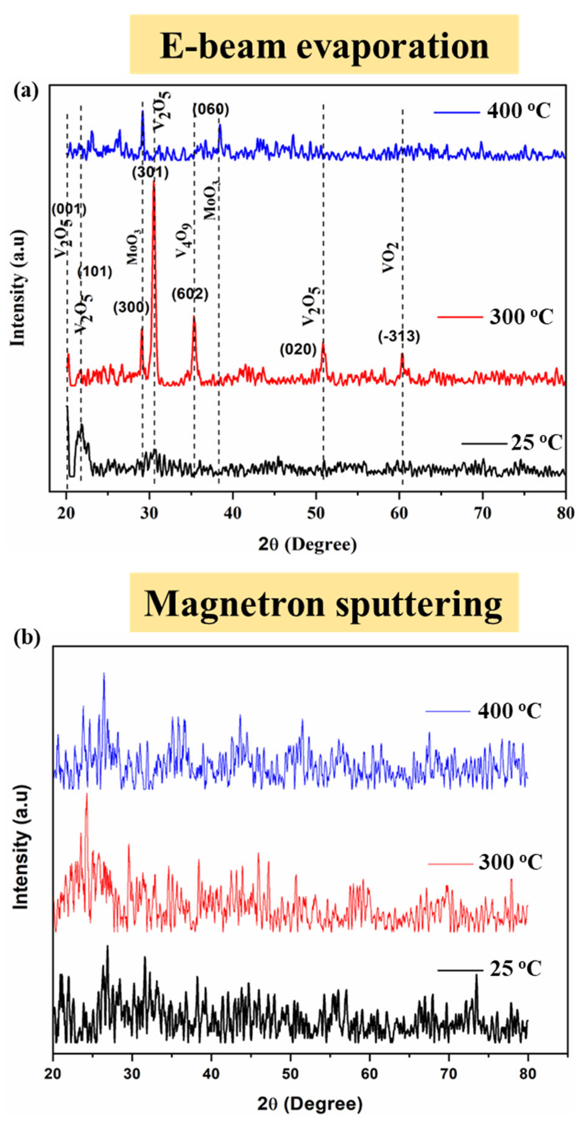
The XRD pattern of V
2O
5 thin films deposited by the e-beam demonstrates the reflection at planes of (001), (101), (020), and (301) following the orthorhombic structure. The peaks are well matched with the JCPD card no (41-1426) for the orthorhombic structure of V
2O
5 with the P
mmn space group, as described by Gandasiri et al. [
20]. Two impurity peaks were observed, which belong to MoO
3 with JCPD card no (21-0569) for MoO
3, in as-deposited and annealed samples. However, the XRD pattern of an as-deposited sample does not contain sharp peaks, and the peak for MoO
3 is not prominent. The peak at the plane of (602) represents the JCPD card no (24-1391) for V
4O
9 as well as (−313) represents the JCPD card no (19-1398) for V
2O
4. There are multiple phases of vanadium oxide present in the samples because, during the e-beam deposition process, the surface melting of the target material causes the breaking of the bonds in V
2O
5 and the dissociation of oxygen from the vanadium oxide, which ultimately disturbs the stoichiometry of the material. Furthermore, the purging of oxygen in the deposition chamber to complete the stoichiometry is another factor of multiple phases in vanadium oxide. Thermodynamically, the stable phases of vanadium oxide are V
2O
5 and VO
2 along with other unstable phases like V
2O
4, V
4O
9, etc., which can be transferred to stable phases over time.
Electron beam evaporated films are non-stoichiometric containing various phases of vanadium oxides (V2O9, VO2) along with MoO2 present in electron beam evaporated samples. Therefore, by increasing the annealing temperature vanadium makes different oxides, which are amorphous in nature, according to their relevant temperature leading to the amorphous surface.
V2O5 thin film possesses an orthorhombic structure with a unit cell volume of 0.092 nm3. The broad diffractions are showing that the crystallite size of V2O5 lies in the nanometer scale range. The crystallographic lattice parameters of V2O5 are a = 1.85 Å, b = 1.85 Å, and c = 6.71 Å with a crystallite size of ~25 nm (determined via the Debye-Scherrer equation).
The XRD pattern of V
2O
5 films deposited by magnetron sputtering is shown in
Figure 1b. As observed, the sputtered films are amorphous before/after annealing. This is due to the high energy of sputtered atoms.
FESEM was performed to evaluate the surface imaging of the fabricated thin films.
Figure 2a–f show the images of as-deposited V
2O
5 thin films deposited by e-beam evaporation and magnetron sputtering at 50 kx magnification. It can be noticed that as-deposited thin films of V
2O
5 deposited via e-beam evaporation or magnetron sputtering consist of small nanoparticles with dense structures. Even at 100 kx magnification, in
Figure 2a, the uniformity and smooth surface of as-deposited V
2O
5 thin films were observed.
After annealing at 300 °C, no significant changes were observed in their morphology
Figure 2b,e, i.e., they show uniform and dense structure. After annealing at 400 °C, the surface morphology significantly changed (
Figure 2c,f). The particles agglomerated to form nanorods in the thin films deposited by e-beam evaporation. In comparison to these thin films, agglomeration can also be observed in magnetron-sputtered thin films. The agglomeration, as depicted by SEM, is basically amorphous, which is consistent with the XRD studies. With the increase in annealing temperature, the film is moving towards crystallinity, but the driving force (temperature) is not sufficient to make it crystalline. The transformation from crystalline phase to amorphous phase is not very common; however, it can take place due to the confusion effect. The constituent atoms simply cannot coordinate themselves into the equilibrium crystalline state before their mobility is stopped. In this way, the random disordered state of the atoms is “locked in”. Actually, magnetron sputtering films are quite flat in comparison with e-beam evaporated films. In our earlier experience, the films deposited by magnetron sputtering shows less roughness in the range of less than 100 nm (the AFM study was not performed in the present case). However, the films as can be depicted by SEM images are quite smooth with less roughness.
SEM images of electron beam evaporated samples show the grains of V
2O
5 as already shown in the XRD pattern with some impurities of other phases such as V
4O
9, VO
2, and V
2O
3. However, due to low contrast, these phases cannot be differentiated [
21]. Magnetron Sputtered films are dense, compact and do not contain any pinhole. Even no peel-off or blister is observed in the films. However, the samples are still amorphous.
EDS was performed to estimate the quantitative and qualitative analysis of our fabricated V
2O
5 thin films either deposited by e-beam evaporation or magnetron sputtering. EDS analysis reflects the presence of vanadium and oxygen in both magnetron-sputtered and electron beam-evaporated samples along with the signals from the substrate as shown in
Figure 3.
Rutherford backscattering spectroscopy (RBS) spectrum of as-deposited e-beam evaporated V2O5 thin film shows the presence of different peaks; the one with the sharp peak demonstrates the V2O5 and the sharp one shows some molybdenum oxide along with the minor peaks that are the sign of substrate elements. The intended thickness of these V2O5 thin films was kept at 150 nm. However, the thickness calculated by RBS was slightly greater than the intended thickness due to the limitations of the crystal quartz monitor and annealing in an open atmosphere. Annealing temperature made the molybdenum peak more prominent and sharper than it was observed in the as-deposited sample. It has also been noticed that elemental concentrations are in good stoichiometric ratios with a very minor concentration of molybdenum.
It can also be concluded that magnetron sputtered thin films are more accurate and uniform with good quality of composition and good control of thickness with no impurity element. Furthermore, the stoichiometry of sputtered films is better than evaporated films as shown in
Figure 4.
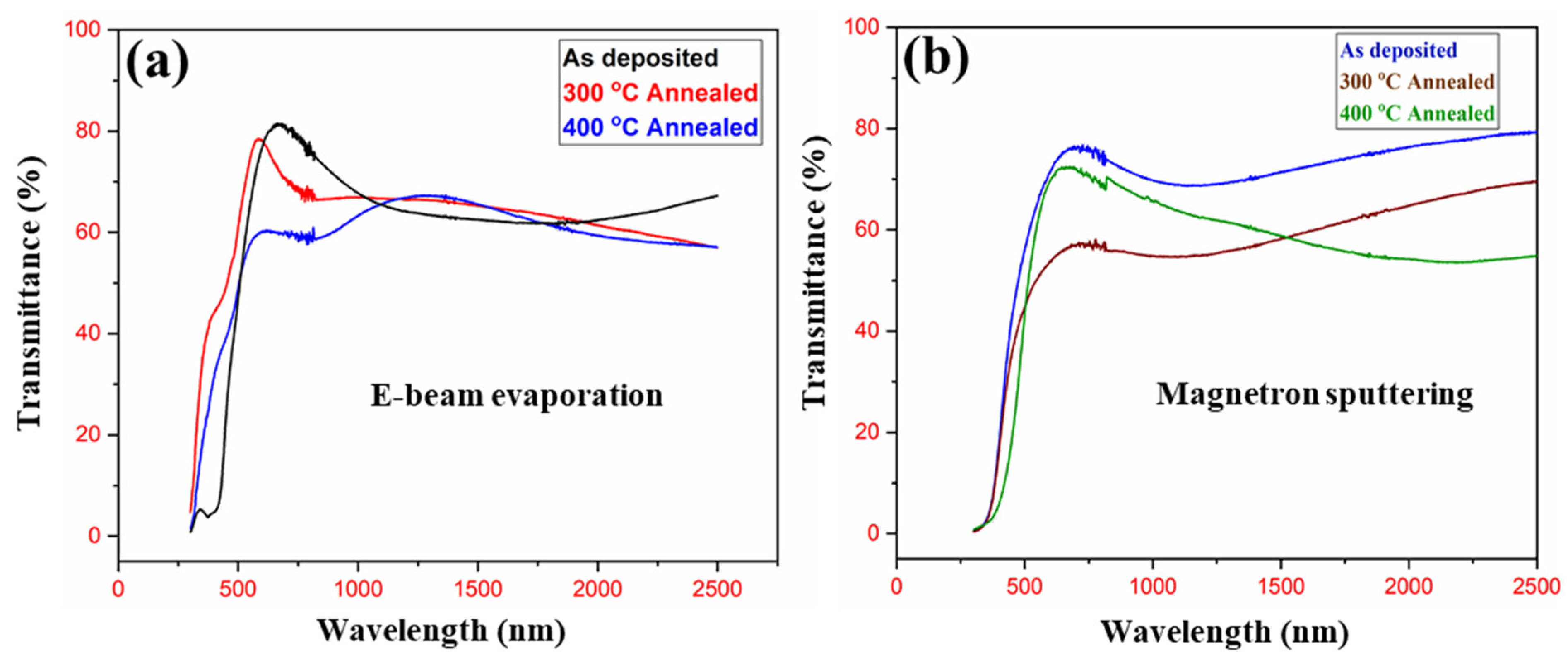
UV-Vis-NIR spectrometer was used to determine the transmittance, reflectance, absorbance, and subsequently, the band gap energy, to compare the optical properties of these thin films.
Figure 5 shows the optical transmittance spectra of the V
2O
5 thin films that lie in the region of 200–2500 nm wavelength. It reveals that transmittance decreases with increasing the annealing temperature due to oxygen defects in both electron beam evaporated and magnetron-sputtered thin films. The interference fringes are also shown in the higher wavelength region, which indicates that neither absorption nor scattering of light occurs beyond the absorption edge. These oxygen defects in both films can contribute to the increase in surface roughness and packing density of these thin films.
The absorption coefficient increases as wavelength decreases. Crystallite size and strain values play an important role in band gap engineering. The band gaps of V
2O
5 thin films deposited by e-beam and magnetron sputtering have been determined using the linear extrapolation of Tauc’s plot. For as-deposited samples, the calculated band gap (
Table 1) values of 2.25 and 2.22 eV for both electron beam evaporated and magnetron sputtered thin films, respectively, were determined which is in agreement with previous reports [
22,
23]. The e-beam deposited V
2O
5 films are showing non-stoichiometry with two band gap structures. The band gap of 2.25 eV belongs to V
2O
5 while the other band gap is related to the synergistic effects of all other phases. Comparably, the magnetron sputtered samples show only a single band gap due to the stoichiometry of the films.
Increasing the annealing temperature from 300 to 400 °C indicates the electron’s excitation across the gap, and the entropy of these electrons, which leads to a decrease in band gap values as shown in
Figure 6. The decrease in band gap is responsible for the structural modifications, an increase in crystalline quality, and a decrease in defect density of V
2O
5 thin films. The band gap values obtained below the semiconductor-to-metal transition temperature are within the reported range of 2.06–2.3 eV illustrating the semi-conductive nature of these thin films [
24]. It can also be seen that the sputtered films are stoichiometric without any impurity phase.
Electrical properties of V
2O
5 thin films, e.g., conductivity, carrier concentration, and mobility were evaluated using Ecopia Hall Measurement System 5000 at room temperature. These electrical properties were determined with the help of Van-der-Pauw approach [
25].
From the results summarized in
Figure 7, the conductivity of the as-deposited e-beam evaporated film was 1.1 × 10
−5 S/m, which is desirable for microbolometer applications [
26,
27]. While for sputtered film, conductivity is shown as 13 S/m with the intrinsically doped carrier concentration which is determined by the Hall measurement technique. The conductivity of V
2O
5 thin films is ~4 × 10
−2 S/m [
22]. The conductivity of sputtered films is more than the bulk value while lower in the case of e-beam. The reduced conductivity is attributed due to the mixed phase and non-stoichiometry of the e-beam films, while a higher conductivity is due to higher mobility and carrier concentration. The reported values of carrier concentration and conductivity are 3.6 × 10
18 [
22] and 4 × 10
−2 S/m [
22], respectively. A desirable microbolometer material has large TCR values with negative TCR at operating temperature [
23]. A conductivity of 1.5 × 10
−5 S/cm is reported for the TCR value of 4.08%/K [
26], which is suitable for microbolometers but increasing the conductivity will lead to negative TCR which becomes more beneficial in case of resistive microbolometers. In the present case, results of electron beam evaporated films show conductivity in the range of 10
−5 S/cm, which is well suited to the literature values, while for magnetron sputtered films, the conductivity is much higher (17 S/cm) in comparison with e-beam evaporated films. Therefore, when it comes to magnetron-sputtered films impurity becomes negligible and films are stoichiometric in nature which increases the conductivity. The higher values of conductivity are, however, more desirable for microbolometers applications. However, in both sputtered and e-beam annealed films, the conductivity increases with increasing the annealing temperature. The increase in conductivity is due to a decrease in defects density, an increase in crystallinity, and more stoichiometry in the films with annealing temperature. Furthermore, the conductivity is strongly dependent on the band gap. Increasing or decreasing the band gap causes conductivity to alter. In the present case, increasing the annealing temperature reduces the band gap (as shown in
Figure 6b), which causes the conductivity to increase [
22]. In the case of e-beam deposited films, the conductivity is low in comparison with sputtered films due to non-stoichiometry and the presence of other phases such as MoO
2, V
2O
9, VO
2 as shown in XRD
Figure 1a. As shown in
Figure 7, the mobility and carrier concentration also increases with annealing temperature, which is the primary reason for the increase in conductivity in annealed films.
Table 2 shows the values of conductivity, mobility, and carrier concentration of V
2O
5 thin films deposited by e-beam evaporation and magnetron sputtering techniques.
4. Conclusions
V2O5 thin films have been prepared by e-beam and magnetron-sputtering techniques onto the soda lime glass substrates. These films were amorphous with magnetron sputtering and crystalline in case of electron beam evaporation.
The obtained coatings were found to be with good uniformity, better adhesion properties, physically stable, and free from the pinhole. A small amount of impurity of molybdenum (Mo) has been observed in electron beam evaporated films.
Rutherford backscattering spectrometry of e-beam as-deposited film revealed a thickness of 177 nm, which was slightly greater than the intended thickness of 150 nm. The increase in thickness has been observed with increasing annealing temperature due to additional oxygen coming from the environment. As-deposited sputtered films show a thickness of 262 nm. The elemental composition shows the presence of vanadium and oxygen measured by EDX and RBS were found to be consistent.
Maximum transmittance of 81% is observed in e-beam as-deposited film while sputtered as-deposited film show a transmittance of 76%. The band gap of as-deposited e-beam and magnetron-sputtered V2O5 thin films are 2.25 and 2.22 eV, respectively. The band gap of the sample annealed at 300 °C is 1.5 for e-beam and 2.19 eV for sputtered films. While for 400 °C, it is 1.41 and 1.81 for e-beam and sputtered films, respectively. The decreasing trend is due to the annealing effect.
Field Emission Scanning Electron Microscope was used to figure out the structural morphology of the V2O5 thin films. It is observed that the surface of as-deposited and 300 °C annealed samples in both e-beam and magnetron sputtered films were compact, dense, and free from pin-holes. However, after annealing 400 °C, the surface morphology is changed in both films and converted into nanorods in e-beam and plate-like structures in the sputtered film.
The Hall measurement test shows that the conductivity of sputtered films is much better than e-beam evaporated thin films. On this basis, it comes to the end that IR sensors can be fabricated using sputtered films, particularly the film annealed at 400 °C.
Magnetron-sputtered thin films provide better adhesion and conductivity, precise control of thickness (as compared to e-beam films), higher mobility, carrier concentration, and are quite uniform. Above all, the magnetron-sputtered V2O5 films are more stoichiometric than e-beam deposited films, which contain impurity phases. However, e-beam films are more cost-effective than sputtered ones, which are relatively expensive. As a whole, sputtered films are better in all aspects than e-beam films.


 ,
, 


