Article

Study of Anodic Film’s Surface and Hardness on A356 Aluminum Alloys, Using Scanning Electron Microscope and In-Situ Nanoindentation

1
Department of Industrial Materials Technology, Production Division, Bay Zoltán Nonprofit Ltd. for Applied Research, Kondorfa utca 1, H-1116 Budapest, Hungary
2
Department of Materials Physics, Eötvös University, Pázmány Péter sétány 1/A, H-1117 Budapest, Hungary
*
Author to whom correspondence should be addressed.
Coatings 2022, 12(10), 1528; https://doi.org/10.3390/coatings12101528
Submission received: 3 August 2022 / Revised: 1 October 2022 / Accepted: 8 October 2022 / Published: 12 October 2022

Abstract

:
The A356 aluminum alloy is a very commonly used alloy in the automotive industry, for parts such as pistons, cylinder heads, and connecting rods, for which the mechanical properties can be effectively increased by anodizing. In this work, oxide layers were formed in oxalic acid solution with defined parameters on A356 aluminum alloy and then studied by using a novel combination of the scanning electron microscope (SEM) and in-situ nanoindentation. The purpose of this research is to understand the relationship between the substrate and the oxide layer by examining its microstructure and nanohardness. Based on the experimental results showing special composite microstructure and corresponding high hardness, this alloy seems to be a good alternative for replacing steel brake disks in an environmentally conscious manner.

1. Introduction

Pure aluminum has excellent corrosion resistance due to the spontaneous formation of a passive aluminum oxide layer on its surface, but it is rarely used on an industrial scale because of its limited mechanical properties. The applied alloying elements can increase the mechanical properties; however, the corrosion resistance of the alloy could decrease [1].
The A356 aluminum alloy is a common Si-containing Al-alloy, which can be characterized by low cost, ease of handling, good combination of strength and ductility, as well as excellent resistance to atmospheric corrosion. The application of Al2O3-reinforced aluminum alloy matrix composites in the automotive and aircraft industries is gradually increasing for pistons, cylinder heads, and connecting rods [2]. In the case of pure Al-Si alloy, if the Si concentration is lower than 12.6 wt.%, both Al dendrites and eutectic phase may be present in the microstructure [3]. Depending on the concentration of Si, Al-Si alloys can be classified into hypoeutectic alloy (Si < 12.6 wt.%), eutectic alloy (12.6 wt.% Si), and hypereutectic alloy (Si > 12.6 wt.%). Si content of Al-Si alloys is responsible for shrinkage and thus improving Al castability [3,4]. The Al-Si alloy may contain other elements such as Mg, Cu, and Fe, for which the eutectic phase may be more complex, containing other intermetallic particles. It is well-known that the addition of a small amount of Mg to Al-Si alloys increases the strength and hardness [5]. In order to get a better corrosion resistance of Al alloys, anodizing is one cost-effective surface treatment to generate a special oxide layer on the surface. Anodizing is an electrochemical process that promotes the growth of aluminum oxide, according to the chemical Equation [1]:
2 A l + 3 H 2 O A l 2 O 3 + 3 H 2
where the part to be anodized is used as an anode in an electrolyte (usually an acidic solution). The process increases the thickness and modifies the structure of the natural oxide layer [6]. The anodizing process forms a nanostructured oxide film, which grows from the base metal as an integral part of the metal and, when properly applied, imparts to the base sample a hard, corrosion- and abrasion-resistant coating with excellent wear properties. Different applications require different morphologies of the oxide layers, which can be varied with the anodizing conditions. When using boric and tartaric acid electrolytes, if the oxide is not soluble, the oxide layer could be thin and nonporous. However, if the anodic oxide is partly soluble in the electrolyte, (for example in oxalic acid) porous oxides are formed. This property allows the coloring of the oxide using organic dyes, pigment impregnation, or electrolytic deposition of various metals into the pores of the coating [7,8].
For wide mechanical properties, nanoporous anodic aluminum oxide (AAO) has become one of the most popular materials with a large potential to develop emerging applications in numerous areas, including biosensors, desalination, high-risk pollutants detection, capacitors, solar cell devices, photonic crystals, template-assisted fabrication of nanostructures, and so on [8].
The thickness of the coating is mostly influenced by the electrical charge passed through the metal/solution interface, temperature, and chemical composition of the electrolyte [9]. The thickness, hardness, and wear resistance of the anode oxide layer on aluminum samples must be of good quality for industrial purposes [10].
In order to obtain the optimal anodized layer, the conditions for the formation of the layer must be known. According to the literature, low temperature and high anodic current density may result in a thick layer [11], but the hardness of the layer may be reduced. The phenomenon can be characterized by an uneven growth of the oxide layer, the result of unbalanced formation and dissolution of the barrier layer at some points [8,12,13,14], which also modifies the color of the layer from grey to black. Furthermore, coating thickness has also a strong influence on the roughness and adhesion of the anodic aluminum oxide [15]. Together with the formation of the oxide layer, the hardness of the anodic film is usually higher than that of the substrate [16].
Contrary to the previous, the thickness of the layer formed at a higher temperature is smaller, therefore a relatively low temperature was chosen for the experiments [17]. Studies available on anodizing of aluminum in oxalic acid solutions show that at temperatures lower than room temperature the growth rate of the oxide is considerably lower than that observed at room temperature [18,19].
A commonly used electrolyte for anodizing is oxalic acid, which is more expensive than sulfuric acid, but it can form thicker and harder layers. Sulka et al. [20] fabricated nanopore arrays by two-step self-organized anodization of aluminum carried out in 0.3 M oxalic acid at room temperature. Stępniowski et al. [21] presented a process, which is a simple and elegant solution for low-cost high-efficiency preparation of nanopores having a diameter lower than 30 nm. They have also used oxalic acid of 0.3 M but at higher temperatures of 35–50 °C.
This work is mainly focusing on the investigation of the microstructure and mechanical properties of anodized, recycled A356 aluminum samples by using the novel combination of the scanning electron microscope and in-situ nanoindentation methods.

2. Materials and Methods

The chemical composition of the untreated sample (A356 Al-alloy) is Al-7Si-0.29Mg in wt.%. Samples to be anodized were rectangular in shape. Figure 1 shows the untreated sample.
Figure 2 shows the schematics of an anodizing cell, where the pre-treated aluminum workpiece is used as the anode connecting to the positive terminal of a DC power supply, and the aluminum cathode is connected to the negative terminal of the supply. The cathode was rectangle-shaped, and the distance of 6 cm between the anode and cathode is the same. In the anodizing process, the main parameters are the composition and concentration of the acid, the temperature, current density, voltage, and the time of the process. The efficiency of the anodization has been increased by controlling the temperature of the electrolyte and stirring it (200 rpm). The constant temperature, which was chosen as 10 °C based on the preliminary experiments, was ensured with the help of a thermostat and continuously monitored with a thermometer.

2.1. Pre-Treatments

In order to remove the natural oxide layer, the samples were ground with 80–2500 grit SiC paper and then polished with Ø7 µm aluminum–oxide paste. The pre-treated samples were then placed in a room temperature 20 g/L phosphate bath for 50 min to remove impurities and then washed with distilled water and alcohol. The output of the sample preparation was checked by measuring the surface roughness, which was determined by using Mitutoyo SJ-201 equipment. The measured roughness (Ra) was under 0.3 µm.

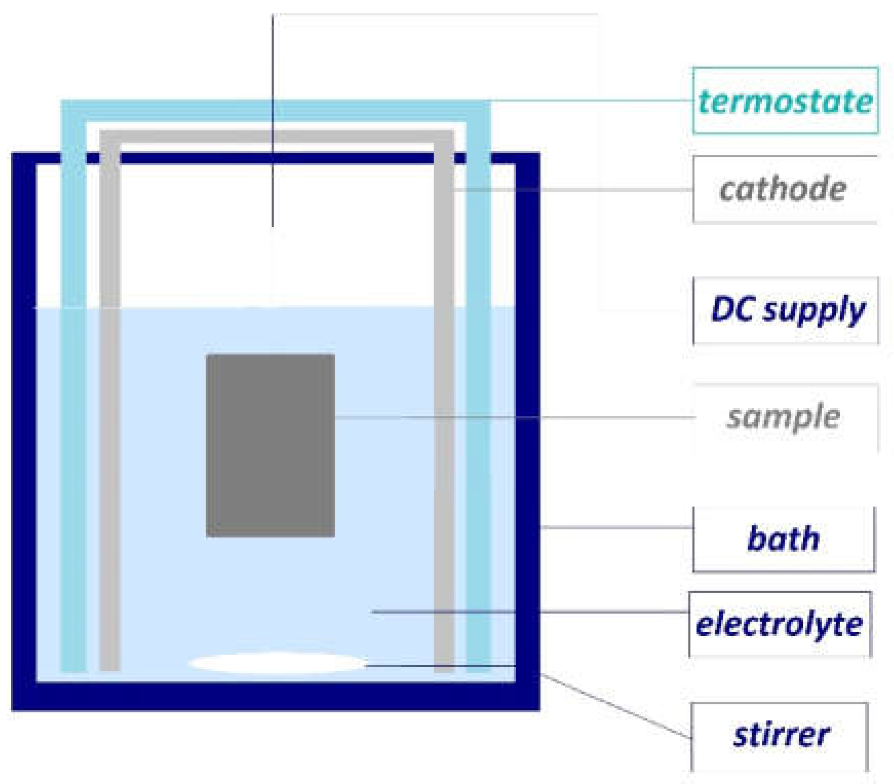
2.2. Anodizing Process

The previous experiments, based on the German anodizing standard [22], provide an oxalic acid that is indispensable in industrial practice–for anodizing. It is well known that in a solution having a given concentration (7–8 wt.%), the increasing rate of the oxide layer is depending on the applied current and time. Therefore, in the first step, some preliminary measurements were performed to see the basic correlations of the surface roughness and layer thickness vs. anodization settings. Based on the preliminary results, considering the acceptable conditions for the feasibility of the experiments and the economic considerations, different samples were anodized in the range of time up to 4 h at current densities from 1 to 6 A/dm2. Following the anodizing process, the samples were rinsed with distilled water and ethanol.

2.3. Surface-Microstructure and Thickness Measurements

Microstructures of the base alloy and the anodized layers were studied by optical microscopy (Keyence VHX-2000) and scanning electron microscopy (SEM), using a TESCAN VEGA electron microscope operating at 5–15 kV and an FEI Quanta 3D FEG machine working at 10–30 kV.
The thickness of the oxide layers is measured in cross-section, by using an optical microscope.

2.4. Microhardness and In-Situ Nanohardness Measurements

One of the important conditions for the use of aluminum in the automotive industry is adequate hardness. So far, hardness measurements have always been made on the anodized surface, which poses several problems. Due to the thinness of the layer, it can be measured only with low force, resulting in small patterns. Since the anodized surface should not be polished, the measurement involves only a high degree of uncertainty. In this work, in addition to standard microhardness measurements, in-situ nanohardness investigations were also carried out.
Microhardness tests were carried out using an UMIS indentation device with a Berkovich indenter and applying a maximum load of 500 mN. In-situ nanohardness measurements were performed using a recently developed mobile nanoindenter [23,24] that can be integrated into an SEM machine. A schematic diagram of the device is shown in Figure 3.
Since this tool can be built into SEM, the indentation can be tracked so that nanohardness measurements can be carried out along the thin cross-section of the oxide layer. In situ nanoindentation tests were carried out in high vacuum mode inside the SEM chamber to allow in situ monitoring of the deformation process. The precision of the indentation depth and the load was ∼1 nm and ∼1 μN, respectively. A more detailed description of the device can be found elsewhere [23].

3. Results and Discussion

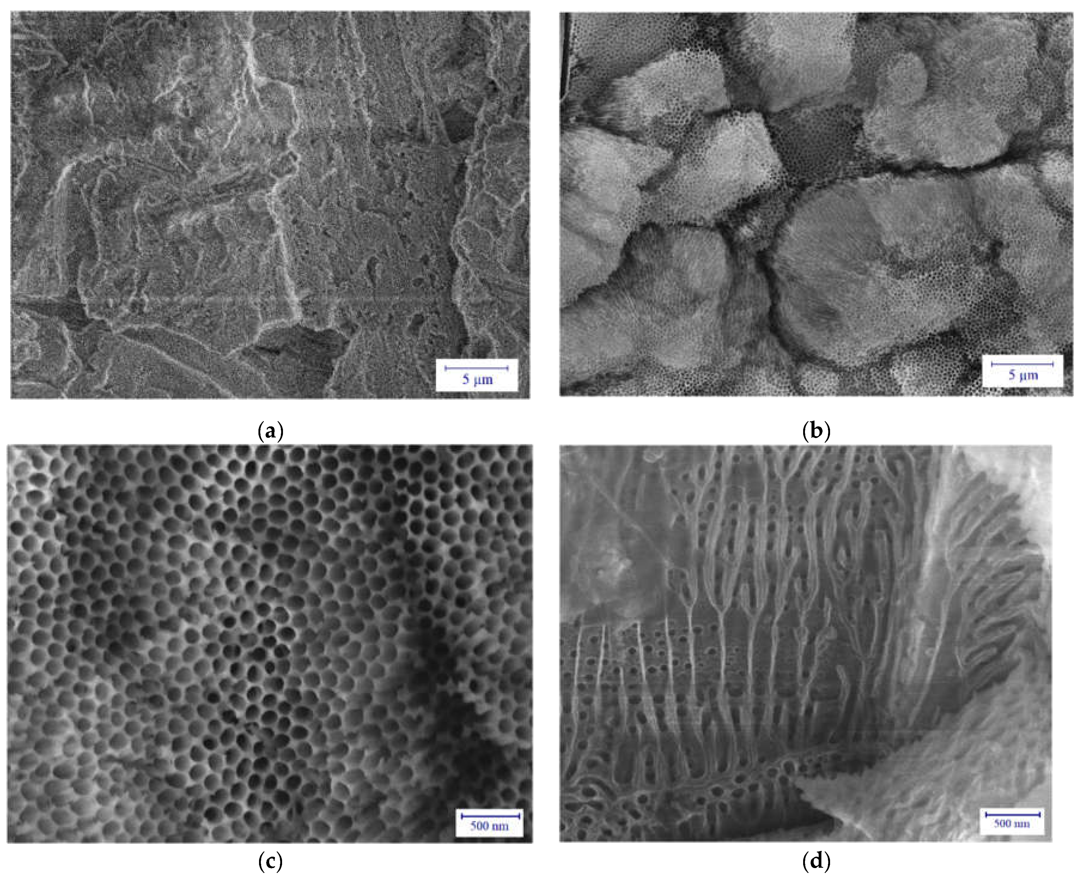
3.1. Microstructure of the Anodized Layers

Figure 4 shows the typically grey color surface of the anodized samples (Figure 4a,b) and the cross-section of an anodized (Figure 4c) containing both the layer and substrate. Using a scanning electron microscope, it can be revealed that the structure of the anodized surface is strongly dependent on the anodizing conditions, mainly on the applied current density, j.
Figure 5 shows the SEM images on two typical microstructures of the anodized surfaces. The application of low current density j = 1 A/dm2 resulted in a relatively compact surface (see Figure 5a). However, when using a higher current density j = 6 A/dm2, an entirely different surface can be observed in the microscopic scale (Figure 5b). In this case, a porous microstructure–similarly to the beehive structure–is formed. The porous image is better seen in Figure 5c, at higher magnification and well observed–as small channels, also in the cross-section of the anodized layer shown in Figure 5d. In terms of porosity, the anodized layer can be considered a composite structure, which may have several advantageous mechanical properties. It should be also noted that the thickness of the anodized layer is strongly dependent on the magnitude of the applied current density. For the anodizing time of 1 h, the thickness of the layer formed at j = 1 A/dm2, shown in Figure 5a is about 40 μm, while that of the layer formed at j = 6 A/dm2, shown in Figure 5b is much higher, about 120 μm.
It is well known that during anodization, the oxide layers are formed by the chemical transformation of the outer layer of the substrate. Thus, the combination of the different physical properties, the chemical composition, and the production technology history of the surface metal layer has an important controlling effect on the properties of the formed layer. Depending on the anodizing conditions, smaller, larger pores may also appear but are not typical [8]. The present experimental results have shown that the application of high anodizing current density will lead to the formation of a well-developed porous layer.
The structure of the formed porous layers can be explained based on the study of Csokan [25] and the Keller–Hunter–Robinson model [8,26]. The oxide film is dielectric in nature, and the current only passes through it until the metal ions leaving the parent metal can diffuse in the oxide-electrolyte boundary phase due to the force field between the electrodes. If an electrolyte capable of dissolving the oxide formed is used, the oxide will loosen at the faults that always occur and pores will form in the layer due to the dissolution caused by Joule heat and electric field. Aluminum oxide is regenerated at the bottom of the pores and may dissolve continuously, but partially. These processes proceed until the substrate is covered with a cover layer of porous but uniform distribution and thickness depending on the treatment time. Therefore, the precondition for the formation and thickening of the anodic oxide layer is the formation of pores, maintaining the continuity of current conduction. Based on this mechanism, we can understand the relationship between the applied current density, the thickness of the resulting layer, and its porous system. Using a high current density, it is likely that the intensity of the dissolution is also higher, leading to the formation of larger channels (pores). Due to this, the anodizing process can take longer, and eventually, a thicker layer can form on the surface of the sample.
Considering again the effect of the current density, Figure 6 shows the change in sample voltage as a function of time (U-t curves) at two different current densities. It can be clearly seen that after the initial rapidly increasing region, there is a significant difference between the two U-t curves obtained for the two current densities. It is well established that with the formation of the oxide layer, the resistance of the sample increases, and therefore the voltage also increases in time at a constant current density (current), regardless of the magnitude of the current density. After a fast, almost linearly increasing region, the voltage continues to increase very slowly but continuously at a low current density, j = 2 A/dm2 (see the blue curve in Figure 6). However, in the case of higher (j = 6 A/dm2) current density, the voltage reaches a maximum value and then slowly but began to decrease. Here, we emphasize that the shape of the voltage-time curve is closely dependent on the mechanism of anodization. To maintain the anodizing process, the formation of pores is required due to the insulating effect of the oxide layer. Applying a low current density (current), only small pores (channels) are formed, which can sustain the anodizing process, but in the meantime, the resistance and thus the voltage continues to increase. At higher current densities (currents), a stronger dissolution can occur, leading to the appearance of larger pores (channels), reducing the resistance and thus the voltage. Presumably, the formation of pores began after the rapid linear region. Similar tendencies observed at low and current densities (or low and high voltages) have been reported before [27,28,29].
Figure 7 shows some further results about the effect of the applied current density and the anodizing time on the thickness of the anodized layers. It can be seen that while anodizing at a constant current density, the thickness, d of the anodized layer seems to be linearly changing with anodizing time, t (see Figure 7a). However, when anodizing for the same time of 1 h (see Figure 7b), the thickness, d of the anodized layer is not changing linearly with the current density, j. It can be supposed that for a certain anodizing time, the change in the layer thickness is strongly determined by the formation of the mentioned pores. At not-so-high current densities, where the dissolution due to Joule heat and an electric field may not be strong enough so the pores did not develop enough to increase the anodizing intensity. Therefore, at lower current densities, the layer thickness formed for a certain time does not appear to depend on the current density. Higher current densities can result in the formation of sufficiently large pores, which can already increase the intensity of the anodization, and thus the thickness of the layer can increase with increasing current density in this region, as shown in Figure 7b. In addition, it is obvious that due to the insulating effect of the anodized layer, the layer will not grow at a certain thickness.

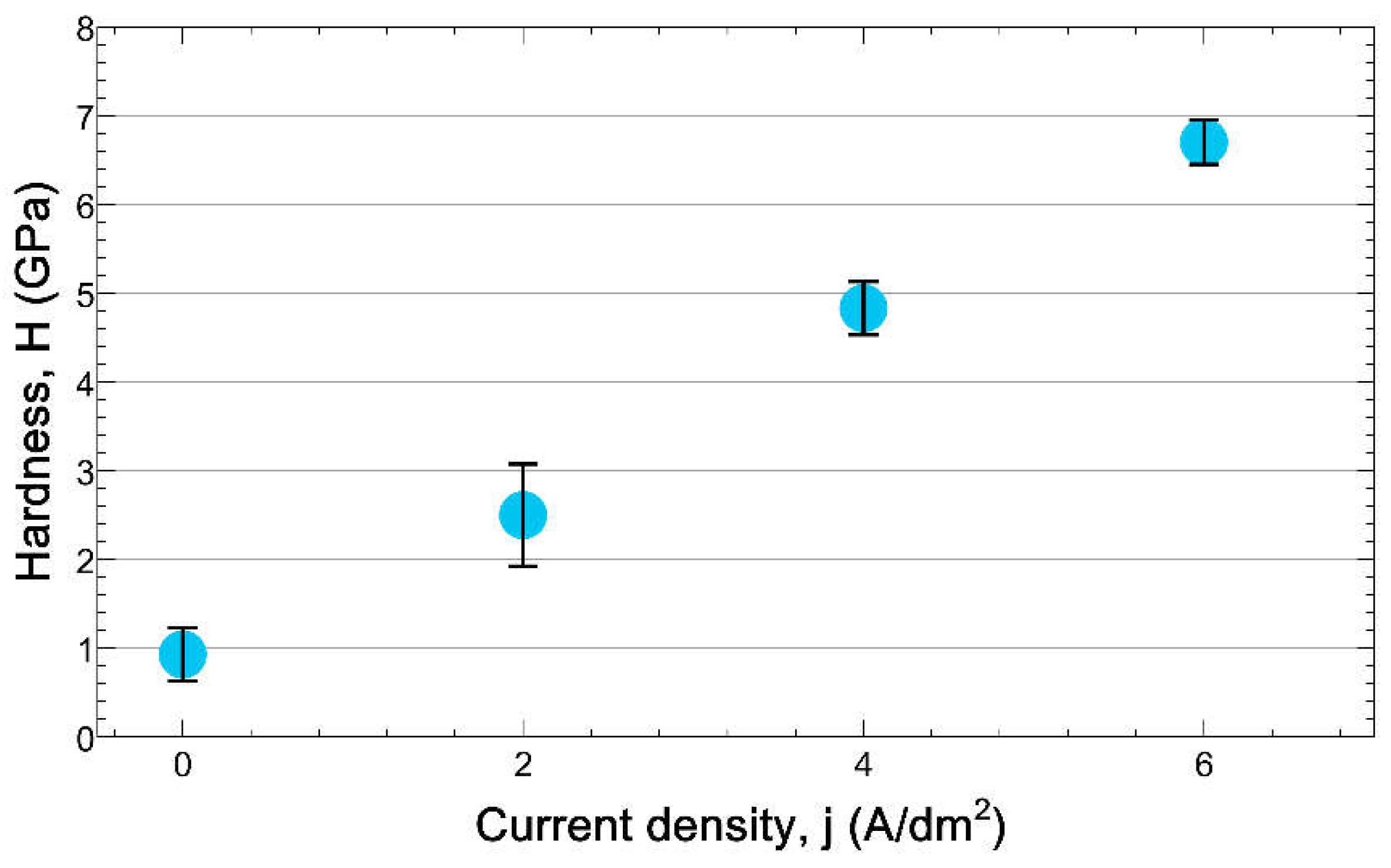
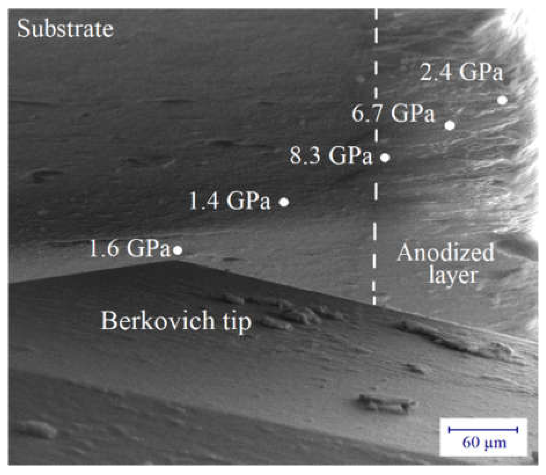
3.2. Microhardness and In Situ Nanohardness Measurements

Together with the observation of the microstructure, the mechanical properties of the anodized layers have also been studied by measuring the hardness both on the surface and on the cross-section of the layers. As it has been mentioned before, since the anodized surface should not be polished, the measurement involves only a high degree of uncertainty. However, the results of microhardness measurements taken on the surface unambiguously show a significant increase in hardness due to the anodizing. While the hardness of the substrate is about 0.6 ± 0.1 GPa, the value obtained on the anodized surfaces is at least four times higher, changing within 2.8 ± 0.8 GPa. It should be noted that the hardness value (0.6 ± 0.1 GPa) of the substrate, obtained in the present work is almost the same as that reported in [30,31].
Our motivation in this work is to understand better the effect of the microstructure of the anodized layers on their mechanical properties. For this purpose, the nano-hardness measurements were carried out on the cross-section of the layers, using the in-situ nanoindenter tool described in point 2.4. To the best of our knowledge, neither hardness measurements on the cross-section of the anodized layer have been reported up to now in the literature with such resolution. Thanks to the development of techniques, the applied load, and displacement, as well as the measuring position, can be easily detected and determined with high accuracy. Figure 8 shows three typical depth-load (h-F) indentation curves taken on the cross-section of the substrate and anodized layer of the two samples having microstructures shown in Figure 5. Considering the tendency of these curves, it can be qualitatively seen that the microstructure of the sample anodized at 2 A/dm2 (characterized by the green curve in Figure 8) is softer than that anodized at 6 A/dm2 (red curve).
Quantitatively, the hardness value, H of samples anodized at different current densities was determined by using the well-known Oliver-Pharr method [32,33] and shown in Figure 9. Experimental results obtained on the cross-section, on the one hand, show the significant hardness increase in the layer relative to that of the substrate (at j = 0 in Figure 9), and on the other hand, also the hardness increase in the function of increasing of the applied current density. Comparing the data shown in Figure 7b and Figure 9, it could also be noted that the hardness of layers is increasing with the increasing layer thickness.
The combination of SEM and indentation allows us to systematically examine the hardness at several points along the thickness of the layer at a given sample, as shown in Figure 10.
It should be mentioned that because of the small thickness, only a small maximum load of about 4 mN was applied in these nanoindentation measurements. As a consequence of the well-known size effect [34,35,36], the nanohardness values are, in general, higher than the corresponding microhardness ones. In every case, the relative change of the hardness of the layer to that of the substrate indicates clearly the strengthening of the anodized layers. As the basic mechanism is not well-known, further investigations are needed to clarify the significant change in the hardness along the anodized layer. Considering the process of the layer formation showing the formation and the dissolution of solid oxide at the substrate, and then the porous structure outwards, presumably, higher porosity (lower material density) can result in lower hardness on the outside of the layer.
Another advantage of the combination of the two measurement methods is the immediate examination of the microstructure under the indentation pattern. Figure 11 shows the patterns corresponding to the indentation curves of the sample anodized at 6 A/dm2 presented in Figure 8 (see the blue and red curves). The larger (see Figure 11a) one is characterizing the substrate and the smaller (in Figure 11b), barely visible indentation pattern was obtained near the middle of the layer. The contour of this Berkovich pattern is shown in the image on the right (Figure 11c). It can be seen that according to the higher hardness, the size of the pattern observed on the layer is much smaller than that on the substrate. Furthermore, it is very interesting to see the fibrous microstructure under and around the small pattern in the layer. These fibers are the pore channels shown in Figure 5. We are convinced that the anodized oxide layer with porous channels, acting as a composite material, are greatly improving the surface hardness, and then the mechanical properties of the anodized samples.

4. Conclusions

Microstructure and mechanical properties of the anodic layer formed on the surface of A356 aluminum alloy were studied by SEM, microhardness- and in-situ nanohardness tests. The main results can be summarized as the following:
  • It was shown that the microstructure of the surface layer of anodized A356 Al alloy can be significantly determined by the magnitude of the applied current density. The application of properly high anodizing current density will lead to the formation of a well-developed porous layer, which can be regarded as a composite structure film.
  • It has been demonstrated that the anodic film effectively strengthens the surface of the Al-based substrate. The hardness of the anodized samples may be six times higher than that of the initial material.
  • The present results, on the one hand, highlight the usefulness of the combination of the SEM and in-situ nanoindentation methods and, on the other hand, suggest that the anodized oxide layer with porous channels, acting as a composite material, not only greatly increases the surface hardness, but may also improve the abrasion resistance of the material. The obtained results are important not only in the basic research but also in the economical application of recyclable Al alloys.

Author Contributions

A.M. and Á.V.: Conceptualization, Writing-Original draft preparation. A.M., Á.V. and D.U.: Investigation, Data curation. N.Q.C.: Formal analysis. Á.V. and N.Q.C.: Writing–review and editing, Supervision. All authors have read and agreed to the published version of the manuscript.

Funding

The research of Bay Zoltán Ltd. was implemented within the framework of the KIC-RADIUS project and Project no. TKP2020-NKA-18 with the support provided by the Ministry of Innovation and Technology of Hungary from the National Research, Development and Innovation Fund, financed under the 2020-4.1.1-TKP2020 funding scheme. The research of NQC was financed by the Hungarian-Russian bilateral Research program (TÉT) No. 2021-1.2.5-TÉT-IPARI-RU-2021-00001.

Data Availability Statement

The data that support the findings of this study are all own results of the authors, not available anywhere.

Acknowledgments

The authors express special thanks to Mark Windisch and to István Groma for their assistance in SEM and nanoindentation investigations, respectively.

Conflicts of Interest

The authors declare that they have no conflict of interest.

References

  1. Zhu, B. On the Influence of Si on Anodising and Mechanical Properties of Cast Aluminium Alloys. Ph.D. Thesis, Jönköping University, Jönköping, Sweden, 2017. [Google Scholar]
  2. Sajjadi, S.A.; Ezatpour, H.R.; Parizi, M.T. Comparison of microstructure and mechanical properties of A356 aluminum alloy/Al2O3 composites fabricated by stir and compo-casting processes. Mater. Des. 2012, 34, 106–111. [Google Scholar] [CrossRef]
  3. Morimoto, K.; Takamiya, H.; Awano, Y.; Nakamura, M. Effects of Si content and gas dissolution on shrinkage morphology of hypoeutectic al-si alloys. J. Jpn. Inst. Light Met. 1988, 38, 216–221. [Google Scholar] [CrossRef] [Green Version]
  4. Eisuke, N.; Koichi, A.; Tatsuya, F.; Sadato, H. Some basic research for thin-wall casting technology. J. Mater. Process. Technol. 1997, 63, 779–783. [Google Scholar] [CrossRef]
  5. Curle, U.A.; Möller, H.; Govender, G. R-HPDC in South Africa. In Solid State Phenomena; Trans Tech Publications Ltd.: Wollerau, Switzerland, 2013; Volume 192, pp. 3–15. [Google Scholar]
  6. Whelan, M.; Barton, K.; Cassidy, J.; Colreavy, J.; Duffy, B. Corrosion inhibitors for anodised aluminium. Surf. Coat. Technol. 2013, 227, 75–83. [Google Scholar] [CrossRef]
  7. Roshani, M.; Rouhaghdam, A.S.; Aliofkhazraei, M.; Astaraee, A.H. Optimization of mechanical properties for pulsed anodizing of aluminum. Surf. Coat. Technol. 2017, 310, 17–24. [Google Scholar] [CrossRef]
  8. Liu, S.; Tian, J.; Zhang, W. Fabrication and application of nanoporous anodic aluminum oxide: A review. Nanotechnology 2021, 32, 222001. [Google Scholar] [CrossRef] [PubMed]
  9. Grubbs, C.A. Anodizing of aluminum. Metal Finish. 1999, 97, 476–493. [Google Scholar] [CrossRef]
  10. Kwolek, P. Hard anodic coatings on aluminum alloys. Adv. Manuf. Sci. Technol. 2017, 41, 35–46. [Google Scholar]
  11. Sheasby, P.G.; Pinner, R.; Wernick, S. The Surface Treatment and Finishing of Aluminium and Its Alloys; ASM International: Materials Park, OH, USA, 2001; Volume 1, p. 231. [Google Scholar]
  12. Bensalah, W.; Feki, M.; Wery, M.; Ayedi, H.F. Thick and dense anodic oxide layers formed on aluminum in sulphuric acid bath. J. Mater. Sci. Technol. 2010, 26, 113–118. [Google Scholar] [CrossRef]
  13. Bensalah, W.; Elleuch, K.; Feki, M.; Wery, M.; Ayedi, H.F. Optimization of anodic layer properties on aluminium in mixed oxalic/sulphuric acid bath using statistical experimental methods. Surf. Coat. Technol. 2007, 201, 7855–7864. [Google Scholar] [CrossRef]
  14. Yokoyama, K. Anodic oxidation of aluminum utilizing current recovery effect. J. Met. Finish. Soc. Jpn. 1977, 28, 314–318. [Google Scholar] [CrossRef]
  15. Aerts, T.; Dimogerontakis, T.; De Graeve, I.; Fransaer, J.; Terryn, H. Influence of the anodizing temperature on the porosity and the mechanical properties of the porous anodic oxide film. Surf. Coat. Technol. 2007, 201, 7310–7317. [Google Scholar] [CrossRef]
  16. Gabe, D.R. Hard Anodizing—What do we mean by hard? Metal Finish. 2002, 100, 52–58. [Google Scholar] [CrossRef]
  17. Diggle, J.W.; Downie, T.C.; Goulding, C.W. Anodic oxide films on aluminum. Chem. Rev. 1969, 69, 365–405. [Google Scholar] [CrossRef]
  18. Choudhary, R.K.; Mishra, P.; Kain, V.; Singh, K.; Kumar, S.; Chakravartty, J.K. Scratch behavior of aluminum anodized in oxalic acid: Effect of anodizing potential. Surf. Coat. Technol. 2015, 283, 135–147. [Google Scholar] [CrossRef]
  19. Voon, C.H.; Derman, M.N.; Hashim, U.; Ahmad, K.R.; Foo, K.L. Effect of temperature of oxalic acid on the fabrication of porous anodic alumina from Al-Mn alloys. J. Nanomater. 2013, 40, 40. [Google Scholar] [CrossRef]
  20. Sulka, G.D. Highly ordered anodic porous alumina formation by self-organized anodizing. In Nanostructured Materials in Electrochemistry; Wiley-VCH: Weinheim, Germany, 2008; pp. 1–116. [Google Scholar]
  21. Stępniowski, W.J.; Bojar, Z. Synthesis of anodic aluminum oxide (AAO) at relatively high temperatures. Study of the influence of anodization conditions on the alumina structural features. Surf. Coat. Technol. 2011, 206, 265–272. [Google Scholar] [CrossRef]
  22. Machu, W. Die Verfahren zur Durchführung der elektrolytischen Oxydation des Aluminiums und seiner Legierungen. In Nichtmetallische Anorganische Überzüge; Springer: Vienna, Austria, 1952; pp. 16–24. [Google Scholar]
  23. Ispánovity, P.D.; Ugi, D.; Péterffy, G.; Knapek, M.; Kalácska, S.; Tüzes, D.; Groma, I. Dislocation avalanches are like earthquakes on the micron scale. Nat. Commun. 2022, 13, 1–10. [Google Scholar] [CrossRef] [PubMed]
  24. Kalácska, S.; Dankházi, Z.; Zilahi, G.; Maeder, X.; Michler, J.; Ispánovity, P.D.; Groma, I. Investigation of geometrically necessary dislocation structures in compressed Cu micropillars by 3-dimensional HR-EBSD. Mater. Sci. Eng. A 2020, 770, 138499. [Google Scholar] [CrossRef] [Green Version]
  25. Csokan, P. Some observations on the growth mechanism of hard anodic oxide coatings on aluminium. Trans. IMF 1964, 41, 51–56. [Google Scholar] [CrossRef]
  26. Keller, F.; Hunter, M.S.; Robinson, D.L. Structural features of oxide coatings on aluminum. J. Electrochem. Soc. 1953, 100, 411. [Google Scholar] [CrossRef]
  27. Sulka, G.D.; Stępniowski, W.J. Structural features of self-organized nanopore arrays formed by anodization of aluminum in oxalic acid at relatively high temperatures. Electrochim. Acta 2009, 54, 3683–3691. [Google Scholar] [CrossRef]
  28. Shimizu, K.; Kobayashi, K.; Thompson, G.E.; Wood, G.C. Development of porous anodic films on aluminium. Philos. Mag. A 1992, 66, 643–652. [Google Scholar] [CrossRef]
  29. Choi, Y.C.; Hyeon, J.Y.; Bu, S.D. Correlation between Self-Organized Pore Formation Behaviors and Current-Time Characteristics in Porous Anodic Alumina: Quantitative Analysis of Voltage Dependence of Pore Morphological Changes. J. Korean Phys. Soc. 2010, 56, 113–119. [Google Scholar]
  30. Gecu, R.; Karaaslan, A. Relationship between nanoindentation and wear properties of stainless steel-reinforced aluminium matrix composite. Tribol. Lett. 2017, 65, 164. [Google Scholar] [CrossRef]
  31. Vencl, A.; Bobic, I.; Arostegui, S.; Bobic, B.; Marinković, A.; Babić, M. Structural, mechanical and tribological properties of A356 aluminium alloy reinforced with Al2O3, SiC and SiC + graphite particles. J. Alloys Compd. 2010, 506, 631–639. [Google Scholar] [CrossRef]
  32. Pharr, G.M.; Oliver, W.C.; Brotzen, F.R. On the generality of the relationship among contact stiffness, contact area, and elastic modulus during indentation. J. Mater. Res. 1992, 7, 613–617. [Google Scholar] [CrossRef]
  33. Oliver, W.C.; Pharr, G.M. An improved technique for determining hardness and elastic modulus using load and displacement sensing indentation experiments. J. Mater. Res. 1992, 7, 1564–1583. [Google Scholar] [CrossRef]
  34. Hector, L.G.; Schmid, S.R. Simulation of asperity plowing in an atomic force microscope Part 1: Experimental and theoretical methods. Wear 1998, 215, 247–256. [Google Scholar] [CrossRef]
  35. Schmid, S.R.; Hector, L.G. Simulation of asperity plowing in an atomic force microscope. Part II: Plowing of aluminum alloys. Wear 1998, 215, 257–266. [Google Scholar] [CrossRef]
  36. Chinh, N.Q.; Gubicza, J.; Kovács, Z.; Lendvai, J. Depth-sensing indentation tests in studying plastic instabilities. J. Mater. Res. 2004, 19, 31–45. [Google Scholar] [CrossRef]
Figure 1. The untreated sample.
Coatings 12 01528 g001
Figure 2. The schematics of anodizing equipment.
Coatings 12 01528 g002
Figure 3. 3D image of in situ nanoindenter.
Coatings 12 01528 g003
Figure 4. Appearance of an anodized sample at j = 1 A/dm2 and 1 h, as (a) visible, (b) under an optical microscope, and (c) optical microscope image on the cross-section showing both the layer and substrate.
Coatings 12 01528 g004
Figure 5. SEM images on the microstructure of the anodized layers, showing (a) a compact surface after anodizing at j = 1 A/dm2 at 1 h, (b,c) beehive-like structure formed at j = 6 A/dm2 for 1 h in different magnifications and (d) the corresponding pipe-structure in the cross-section of the anodized layer shown in (b,c).
Coatings 12 01528 g005
Figure 6. Anodic potential of samples as a function of time at low and high current densities.
Coatings 12 01528 g006
Figure 7. The thickness of layers anodized (a) for different times at j = 2 A/dm2 and (b) at different current densities for 1 h.
Coatings 12 01528 g007
Figure 8. Indentation curves obtained on the cross-section of an anodized sample anodized at different current densities for 1 h.
Coatings 12 01528 g008
Figure 9. The hardness, H obtained on the cross-section of samples anodized at different current densities for 1 h.
Coatings 12 01528 g009
Figure 10. Hardness values on the substrate and along the thickness of an anodized layer (j = 6 A/dm2, t = 1 h), obtained by using the combination of SEM and nanoindentation.
Coatings 12 01528 g010
Figure 11. Indentation patterns on (a) the substrate and (b,c) at the middle of the anodized layer, obtained by using the combination of SEM and nanoindentation.
Coatings 12 01528 g011
Publisher’s Note: MDPI stays neutral with regard to jurisdictional claims in published maps and institutional affiliations.

