Article

Mechanism of Chemical Bath Deposition of CdS Thin Films: Influence of Sulphur Precursor Concentration on Microstructural and Optoelectronic Characterizations

by
Asmaa Soheil Najm
1,2,*,
Hasanain Salah Naeem
3,
Duaa Abdul Rida Musa Alwarid
4,
Abdulwahab Aljuhani
5,
Siti Aishah Hasbullah
6,
Hiba Ali Hasan
7,
Kamaruzzaman Sopian
8,
Badariah Bais
1,
Heidar J. Al-Iessa
9,
Hasan Sh. Majdi
4,
Abbas J. Sultan
2 and
Hazim Moria
10
1
Department of Electrical, Electronics and System, FKAB, Universiti Kebangsaan Malaysia (UKM), Bangi 43600, Malaysia
2
Department of Chemical Engineering, University of Technology, Baghdad 10066, Iraq
3
Faculty of Pharmacy, University of Al Muthanna, Samawah 66001, Iraq
4
Department of Chemical Engineering and Petroleum Industries, Al-Mustaqbal University College, Babylon 51001, Iraq
5
Department of Chemical Engineering Technology, Yanbu Industrial College, Yanbu Al-Sinaiyah City 41912, Saudi Arabia
6
School of Chemical Sciences and Food Technology, Faculty of Science and Technology, Universiti Kebangsaan Malaysia (UKM), Bangi 43600, Malaysia
7
Department of Pharmacognosy and Medicinal Plants, College of Pharmacy, Mustansiriyah University, Baghdad 10053, Iraq
8
Solar Energy Research Institute (SERI), Universiti Kebangsaan Malaysia (UKM), Bangi 43600, Malaysia
9
Oil Exploration Laboratories, Baghdad 10053, Iraq
10
Department of Mechanical Engineering Technology, Yanbu Industrial College, Yanbu Al-Sinaiyah City 41912, Saudi Arabia
*
Author to whom correspondence should be addressed.
Coatings 2022, 12(10), 1400; https://doi.org/10.3390/coatings12101400
Submission received: 5 July 2022 / Revised: 9 September 2022 / Accepted: 13 September 2022 / Published: 26 September 2022
(This article belongs to the Special Issue Coatings and Interfaces II)

Abstract

:
In this study, we aimed to improve our understanding of the response mechanisms associated with the formation of CdS thin films. CdS thin film remains the most valuable option for many researchers, since it has shown to be an effective buffer material for film-based polycrystalline solar cells (CdTe, CIGSe, CZTS). We performed experimental and numerical simulations to investigate the effect of different thiourea concentrations on the characteristics of the CdS buffer layer. The experimental results reveal that an increase in thiourea concentrations had a direct effect on the optical results, with bandgap values ranging from (2.32 to 2.43) eV. XRD analysis confirmed that all deposited films were polycrystalline, except for [1/0.75], where there is no CdS formation. Electrical studies indicated that CdS with a molar ratio of [Cd]/[S] of 1 had the maximum carrier concentration (3.21 × 1014 cm−3) and lowest resistivity (1843.9 Ω·cm). Based on the proposed mechanism, three kinds of mechanisms are involved in the formation of CdS layers. Among them, the ion-by-ion mechanism has a significant effect on the formation of CdS films. Besides, modelling studies reveal that the optic-electrical properties of the buffer layer play a crucial role in influencing the performance of a CIGS solar cell.

1. Introduction

Semiconductor thin films play an important role as a buffer layer and as absorbent in photovoltaic devices owing to the ability to control the electrical conductivity of the films [1]. The common criteria for the optimal buffer layer is often defined as having a wider energy bandgap, a smooth surface, and a free pinhole film with a thickness of between 50 and 100 nm [2,3,4]. Cadmium sulphide thin films (CdS) are still extensively employed as an n-type buffer layer, even though other possible and emerging materials are currently being improved and evaluated as a prospect buffer layer [5,6]. Its benefits involve significant optical transmission, bandgap tunability, considerably low-cost synthesis options, and compact crystallographic cell structures owing to its direct bandgap (2.42 eV) and high absorption coefficient of 104 cm−1 [7,8,9]. It is no wonder that CdS thin film has many uses, from optoelectronics to solar cells to LEDs to photonics devices to transistors, and beyond [10].
CdS thin films were synthesized using a variation of techniques, for instance; electrodeposition (ED) [11], physical vapour deposition (PVD) [12], spray pyrolysis [13], successive ionic layer adsorption and reaction [14], chemical precipitation [15], and chemical bath deposition (CBD) [16]. Altogether they are effective, but have some restrictions; others need high temperatures like Chemical Vapor Deposition Method, or use toxic agents such as sol gel method, and low reproducibility like sputtering. Of such techniques, CBD is the simplest, low cost, and is a low temperature deposition technique [17]. In addition, CdS films grown by CBD method demonstrate photoconductivity and coverage properties [18].
The rate of reaction affects the structure and electrical features of the thin film formation. In general, the CBD process depends on chemical reactions occurring at the interface between the solution and the substrate. The exact mechanisms and the appropriate methodology are still topics of discussion [19,20,21,22]. Previous study have suggested an ion-by-ion growth process from activation energy studies and have hypothesized that homogeneous precipitation is a chemical determining step in film improvement [23]. While Kaur et al. [24] proposed that initial adherence to the substrate surface occurs by cluster-by-cluster deposition of CdS particles in bulk solutions, subsequent adhesion of cluster-by-cluster precipitation of CdS particles from solution occurs under some conditions. The aim of studying CBD-CdS mechanisms is to identify the formation process of CdS thin films that is suitable to fabricate chemically deposited photovoltaic (PV) materials. More specifically, the specific mechanism of surface reaction was proposed in this work, which was based on the formation and absorption of intermediates on the substrate surface, as well as the assumption of their decomposition. This mechanism is assumed to be the preliminary step in the formation of CdS thin films.
Several studies have been performed to optimize factors such as temperature, deposition time, pH, and concentrations of different reagents during the CBD process to produce high-quality CdS thin films [25]. To prepare CdS thin films along this way with efficient optical and electrical characterization, it is important to monitor the molar ratio of [Cd]/[S] throughout the synthesis process due to the photoconductivity of the deposited CdS films variations with (Cd/S). However, only a limited study with differences in the [Cd]/[S] ratio has been reported so far. Jadhav et. al noticed that the photoconductivity of chemically deposited CdS films is highest when Cd/S ratio is 1:0.2. [26]. Xiao and team members synthesized CdS nanocrystals in a single step and evaluated the effect of the Cd/S molar ratio on the photoluminescence of CdS samples. They observed that with the rise in the Cd/S molar ratio, the emission intensity of the surface defect states improved significantly and achieved the highest value, while the (Cd/S) molar ratio was 2.0 [27]. Yuan et al. considered the influence of this ratio on the particle size and photocatalytic characteristics. They found that the excess sulphur in CdS samples resulted in larger particle size [28]. According to Pandya et al., decreasing the (Cd/S) to 0.8 led to an increase in crystallite size in the CdS thin films. Beyond this point, however, a further decrease in the molar ratio resulted in smaller crystallites sizes [9]. Kakhaki et al. (2022) observed that the value of photosensivity in samples grown using the CBD approach is significantly dependent on the thickness of the film, the quantum confinement effect, and the quantity of sulphur vacancy [29].
The aim of the research is to investigate the impacts of utilizing various sulphur salt concentrations on CdS thin films prepared via the CBD process in order to study its effect in terms of optical, structural, morphological, and electrical properties. The targeted values of the desired properties of the CdS thin films demonstrate that, by adjusting the thiourea concentrations, it is possible to provide a stable arrangement that promotes the formation of hexagonal phase, in addition to direct optical results close to the bulk bandgap. Thus, due to the fundamental relation between the optical and physical characteristics of the films, this interaction has a greater effect on the morphology of the films and the electrical characterizations of semiconductors. The expected CdS thin film growth mechanisms through the CBD process were also elucidated. As the control of the reaction mechanism is important, the change in the concentration of thiourea led to a change in most of the reaction properties and mechanisms responsible for the formation of the final product. Moreover, to compare the performance of the different salt concentrations, numerical modelling has been simulated to explore the impact of the [Cd]/[S] as a buffer layer on the PCE of CIGS film solar cells.

2. Methodology

2.1. Experimental

CdS thin film was prepared according to our previous work [30] by using ultrasonically cleaned and degreased soda lime glass substrates of size 25 mm × 25 mm. The key precursors for CdS are aqueous solutions from Cadmium Sulphate (CdSO4, Aldrich, purity 98%) and Thiourea, (SC(NH2)2 Merck, ≥98%), Table 1.
Firstly, we placed ~350 mL of DIW water in the clean growth beaker. Then, 20 mL of NH4OH solution was added to the growth beaker. A magnetic stirrer was placed inside the growth beaker and the stirring speed was set to 360 rpm, and heated until it reached 80 °C. The substrates were introduced to the bath once its temperature stabilized. Secondly, in a separate beaker that contained CdSO4 powder, 20 mL NH4OH solution was added and placed in the ultrasonic bath for 10 min. Thirdly, in another separate beaker, 10 mL DI water was added to the thiourea powder and also put in the ultrasonic bath for 10 min. At the end of the sonication process, the contents of the Cd salt beaker were first added to the growth beaker. After 3 min, the thiourea solution was then added to the chemical bath. The final solution volume was 400 mL (350 mL DIW + 20 mL NH4OH mixed with CdSO4 + 10 mL DIW mixed with thiourea + 20 mL NH4OH added to growth beaker). The pH was set to be 9. Afterwards, the reaction time was set to be 30 min. In the following step, thiourea concentrations varied by: 0.001, 0.0015, 0.002, 0.01, and 0.05 M, to adjust the molar ratio of sulphur source (SC(NH2)2 to the cadmium source (CdSO4). The molar ratios of [Cd/S] were used for [1/0.5], [1/0.75], [1/1], [1/5], and [1/25] respectively. For the first concentration we adjusted at 0.001 M, there was no reaction, therefore [Cd/S] at [1/0.5] was neglected. Figure 1 shows the CBD process.

2.2. Simulation

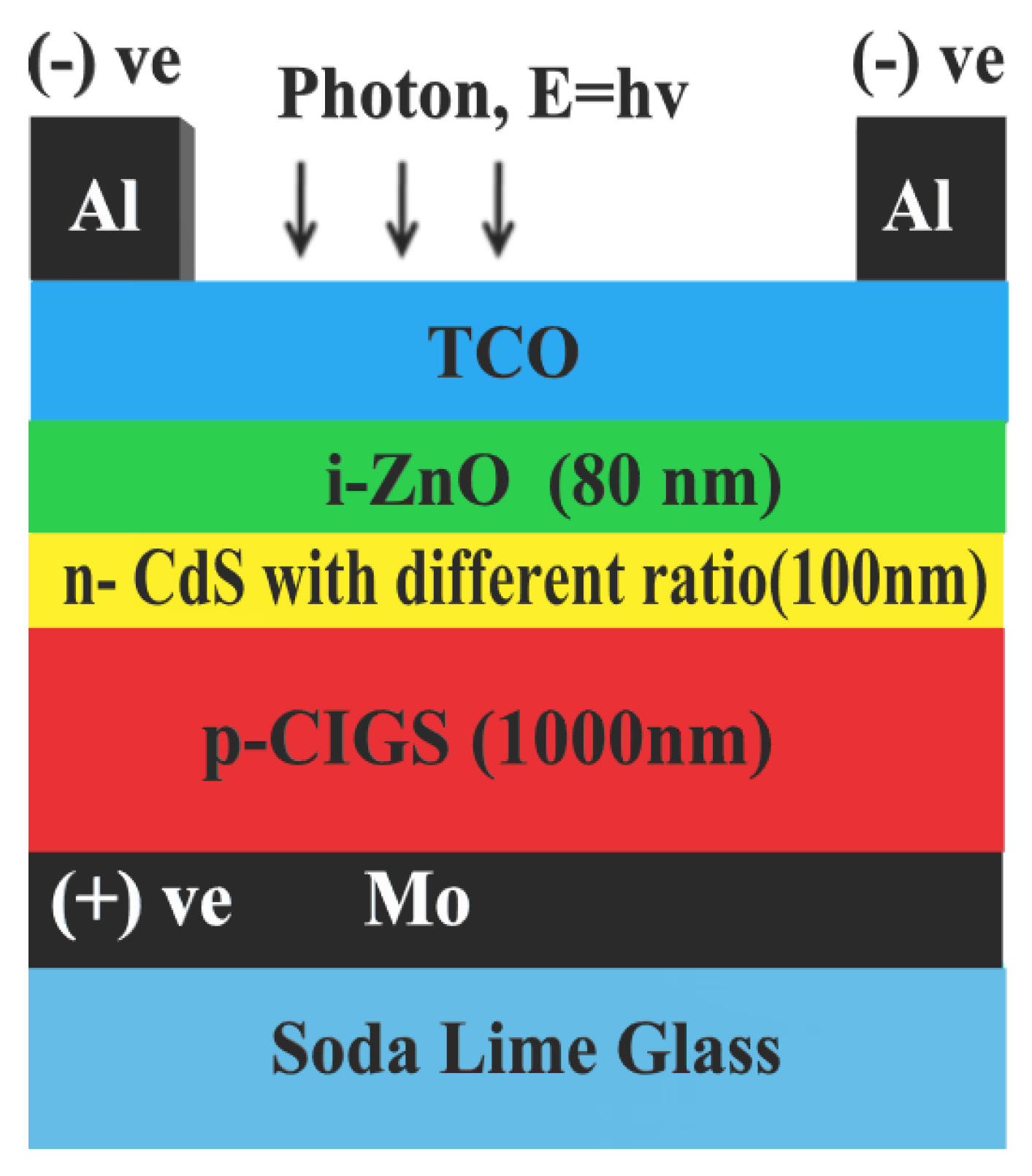
In order to better understand the behaviour of solar cells, numerical modelling can be used to better understand how to modify fabrication parameters in order to maximize cell performance. Researchers from the University of Gent, led by Marc Burgelman, developed and maintained the SCAPS-1D program, which was used in this numerical simulation study [31]. This software was used to simulate the effect of varying [Cd]/[S] ratios on the overall performance of thin film photovoltaic devices. Figure 2 depicts the general device structure used in this work and afterwards simulated in SCAPS.
Material property for each layer and the appropriate theories background are included below in order to provide a reasonable explanation for the choice of material and hetero-interface electrical characteristics, as indicated in Table 2 and Table 3.
Indeed, SLG substrate effects on heterojunction band energy arrangement were not taken into consideration in the simulation because of limitations in the software. Table 2 summarizes the defect characteristics for all relevant layers. The thickness of buffer layer was maintained at 100 nm, and the temperature was set as 300 K in all scenarios. On top of this transparent conducting oxide layer was a metal electrode for the front contact, which was put on an 80-nm thick layer of n-ZnO (TCO). The series resistance parameter was calculated using resistivity values obtained from the hall effect. AM1.5G-1 Sun was used as an illumination bias since it has an integrated power density of 1000 W/m2. Interfacial recombination was not included in this work because of the focus on optical and electrical characterisation of the buffer layer, as well as the buffer layer’s appropriateness for CIGS.

2.3. Characterization

Optical properties of the samples were achieved using a Perkin-Elmer Lambda 950 UV/VIS/NIR spectrometer (Manufacturer PerkinElmer, Inc., Buckinghamshire, UK). The respective bandgap was computed from the obtained absorbance spectrum [35]. The structural properties were tested at room temperature via BRUKER aXS-D8 Advance diffractometer with Cu-Kα radiation wavelengths, λ, of 1.5408 Å. XRD patterns in the 2ϴ range from 10° to 80° were obtained with a step size of 0.02°. A Hitachi SU1510 Scanning Electron Microscope (SEM) was employ for visualizing the surface morphology and the cross section of the samples (Manufacturer Hitachi High Technologies America, Inc., Schaumburg, IL, USA). Finally, the electrical properties were measured using a 0.57 T magnetic field and 45 nA probe current using HMS ECOPIA 3000 Hall Effect measuring device (Bridge Technology, Boise, ID, USA).

3. Results and Discussion

3.1. XRD Studies

In order to determine the crystal structure of CdS thin films, XRD patterns were employed. The samples were scanned from 2θ angle of 10° to 80°. Both cubic and hexagonal phases are the main forms of CdS phases control the electrical characterizations. As a result, it can be deduced that the predominance of one phase (i.e., hexagonal or cubic) over the other forms a distinction in electrical characteristics [36]. In addition, it is difficult to define the specific identity of the CdS film crystal structure, if the film is only hexagonal or essentially cubic or a mixture, since all of them have similar XRD diffraction peak angles [37,38].
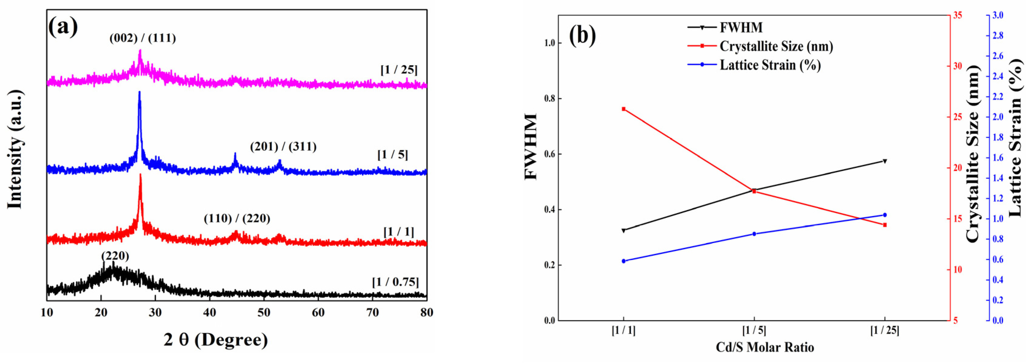
Figure 3a shows that the X-ray diffraction spectra for (Cd/S) values of [1/1], [1/5], and [1/25] show peaks at 2θ = 27.2°, 44.6°, 52.8°, that were matched to (111), (220), and (311) plane of cubic structure (JCPDS-89-0440) or (002), (110), and (201) plane of hexagonal structure (JCPDS No. 01-077-2306). Throughout the situation of a thin-film solar cell, the hexagonal phase of the buffer layer is recommended over the cubic phase due to its stability, wider bandgap, and lower mismatch of the lattice parameters [39].
At [1/0.75] ratio, apart from the dominant peak shift, an evident widening pattern and drop in intensity of the prominent peak is observable. The diffractogram indicated that some of the Sulphur and Cd did not react and appear as peaks at 2θ = 22.2°. The peak at 2θ = 22.2° was matched to Orthorhombic Sulphur (JCPDS-03-065-1436) with a preferred orientation along the (220) plane. This deterioration of CdS crystallinity appeared due to two reasons. Firstly, the decreased sulphur content in the precursor solution, and secondlym the surface adsorption of the intermediate complexes [Cd(NH3)4]2+ and Cd(OH)2 which formed in the solution. Conversely, with analysis of the samples prepared from [1/25] ratio, a large amount of sulphur ions was released into the chemical bath and resulted in their adsorption on the surface of CdS and among film layers, resulting in the film thickness being enough to generate a detectable XRD signal. The crystallite size for both [1/1] and [1/5] samples is bigger under the same growth conditions because of the regular deposition of CdS (Kindly check mechanism part).
The average crystallite sizes of different [Cd]/[S] ratios were estimated from the predominant (002/111) diffraction peak via Debye–Scherrer equation [40]
D = 0.94 λ B cos θ
D is the mean crystallite size, λ = 1.5408 Å is the x-ray wavelength, θ is the Bragg diffraction angle, and B is the full width at half maximum (FWHM) of the diffraction peak, respectively. d-spacing can be evaluated for all samples from the position of the highest peak at 27.2°, regarding the Bragg equation;
n λ = 2 d sin θ
Whereas, n is the diffraction order, λ is the incident wavelength of X-ray, θ is the diffraction angle, and d is the distance between the planes parallel to the axis of incident beam. The calculated crystallite sizes with the d-spacing are given in Table 4.
Table 4 shows that all samples have crystallite sizes (14.4–25.8 nm), suggesting that the polycrystalline CdS films are synthesised from nano-crystal particles. Lattice strain was determined by computing Equation (3) [41];
ε = B 4 tan θ
Figure 3b is the variation concerning FWHM, strain, and crystallite size corresponding to different [Cd/S] ratios. Lower strain value implies higher crystallinity [42]. As the concentration of S2- is increased, the strain decreases in the [1/1] sample but increases slightly in the [1/5] and [1/25] samples. This is due to the passive recrystallization process in the polycrystalline thin films, as well as the movement of interstitial Cd atoms from within the crystallites to the grain boundaries, which dissipates and results in the strain increasing slightly [43]. The same trend can be observed in FWHM. Alternatively, the opposite pattern is seen in the crystallite size.

3.2. Optical Properties

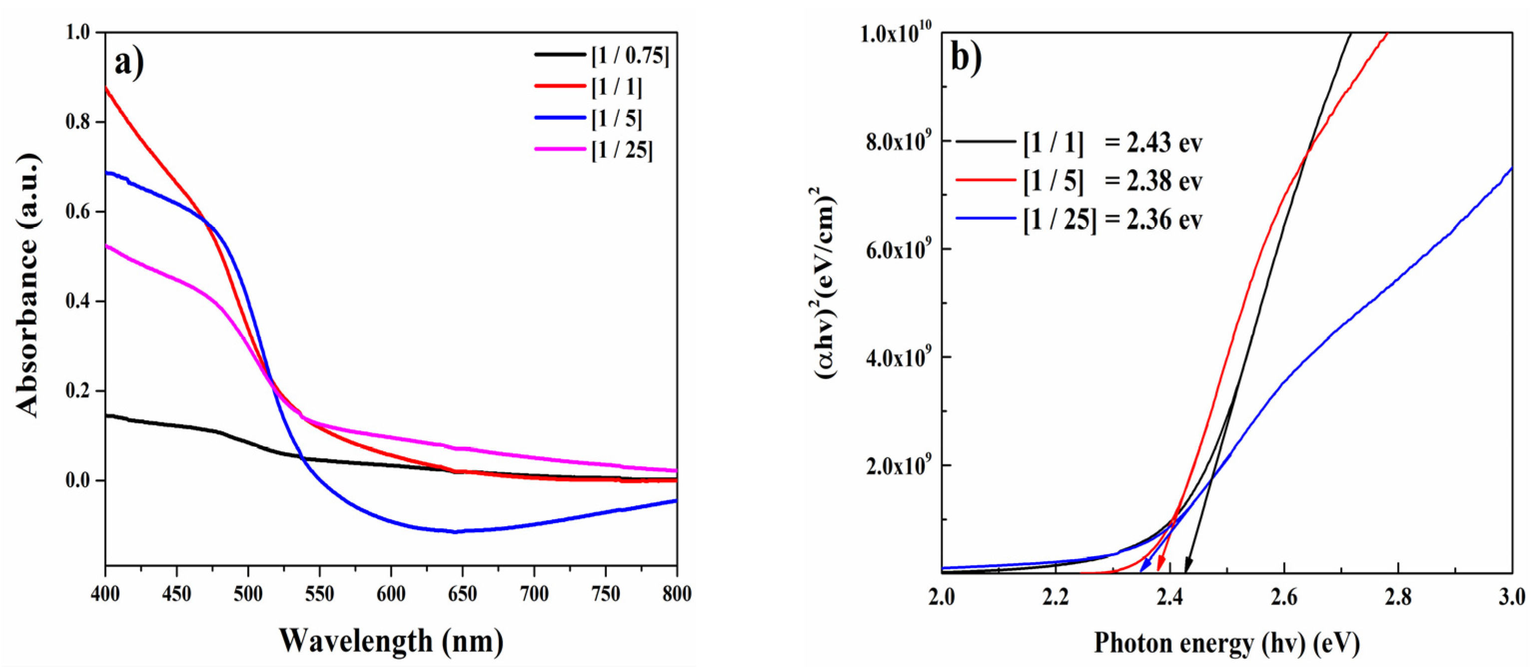
In order to confirm the maximum sunlight is able to influence the absorber layer in solar cells, it is crucial to use thin films with sufficient transparency as the buffer layer. Figure 4a.
The variance of the absorption edge slope suggests that film absorbency improves with increasing in the concentration of S2−, and to some extent, the effect is reversed. Accordingly, sample [1/1] was found to have the highest absorption spectra at 530 nm, which is desirable for buffer layer application. The absorbance (along the vertical axis) is simply a measurement of the quantity of light absorbed. The higher the value, the higher the absorption of a certain wavelength. The active layer collects incident light to form photocarriers, which are significantly impacted by the buffer layer. Because the window layer’s refractive index impacts its reflectivity, its optical band gap and optical absorption coefficient determine its light transmission. The buffer layer with an appropriate index of refraction and high light transmission will reduce light reflection and self-absorption and enhance the amount of light flowing through the buffer layer for the solar cells to absorb. Thus, the increase in the optical path of incident light and the light absorption capacity led to an increase in the carrier concentration yields to higher carrier collection at the front contact and thus a higher JSC in order to enhance the PCE. The reduction in the density of the grain boundary can be attributed to lower optical scatter [44,45].
By using the Tauc plot displayed in Figure 4b, CdS optical bandgap was determined. The dispersion relationship along the semiconductor bandgap absorption edge is used to obtain optical bandgap values [46]. The optical bandgap (Eopt) and optical absorption coefficient (α) are related in the transition direct semiconductor, as follows:
α h v = B ( h v E g ) 1 2    
As α is the coefficient of absorption, hv is the photon energy, Eg is the direct bandgap energy, B is a Boltzmann constant, and 0.5 is a constant used for direct bandgap semiconducting material. Extrapolation of the linear part of the Tauc plots to the horizontal axis intercept indicated that the bandgaps are between 2.32 to 2.43 eV. This range is considered suitable for buffer layer materials in PV applications [47]. The optical bandgap of sample [1/1] is slightly higher than other samples and can be consider as the optimum one. It is possible that, as through the deposition phase where the CdS matrix is formed, additional S vacancies found in sample [1/5] and [1/25] affect a shift in film stoichiometry, based on the change in the defect density induced by the stoichiometry. Those defects can also be responsible for the decrease of the bandgap energy value [9,48]. In this principle, the bandgap energy variations of the crystalline value are expressed.
The optical absorption spectrum of semiconductor materials plays a significant role in supplying fundamental knowledge on its optical properties [49]. The key parameter is the bandgap of the material, which assists in investigate the basic absorption, electron–hole pairs, and light energy generation [50]. The absorption spectra are classified into three primary regions: absorption edge area, strong absorption region (identify the optical energy gap), and weak absorption zone with an exponential dependence on photon energy, known as the Urbach tail [51]. Urbach tail is greater in low crystalline, disorderly, and amorphous substances since they have localized states which extended in the bandgap [52]. The spectral dependency of absorption coefficient (α) and photon energy ( h v ) is identified as the empirical rule for Urbach in the low photon energy range as follows:
α = α ° exp ( h v / E U )          
where α ° is a constant and EU represents the band tail, that is dependent upon temperature [53]. By applying logarithm to both sides of the equation, a straight line equation can be obtained as follows.
ln α = ln α ° + ( h v E U )            
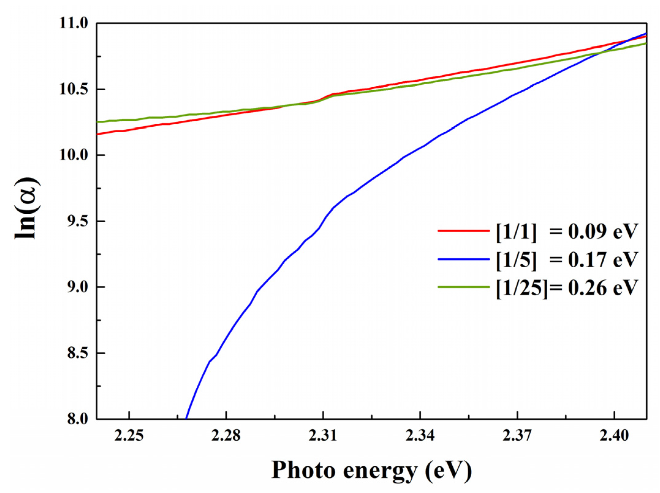
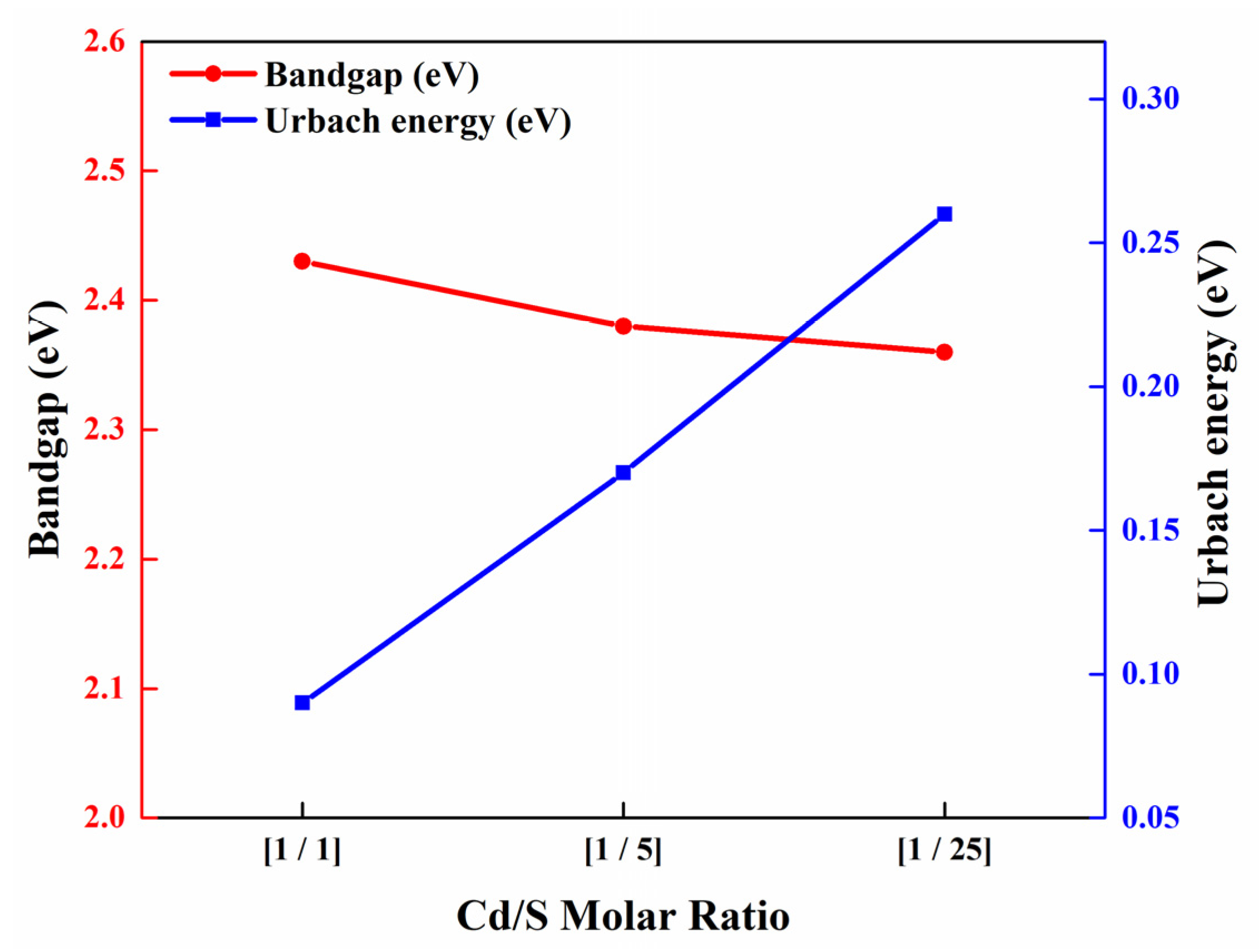
Hence, the Urbach energy (EU) of CdS thin films is able to be determined by plotting in ( α ) against the incident photon energy ( h v ), as displayed in Figure 4b, and computing the slope of the straight line, Figure 5.
Urbach energy of CdS thin films declines slightly from 0.26 eV to 0.09 eV as the molar ratio decreases, showing the typical inverse dependence with energy bandgap. Although sample [1/25] showed higher Urbach energy than sample [1/5], that is possibly due to the excess of sulphur.
Figure 6 shows that the lowest value of Urbach energy is associated to both ratio [1/5], and [1/1], which is suggestive of better crystallinity of the samples and low defects, which is also agreed by lower strain value results. This finding provides useful information to the scientific community—that it is important to control the molar ratio of [Cd]/[S] through the CBD process which is intended for photovoltaic applications.

3.3. Surface Morphology

Scanning electron microscopy (SEM) is an effective technique for examining sample surface morphology [54], Figure 7.
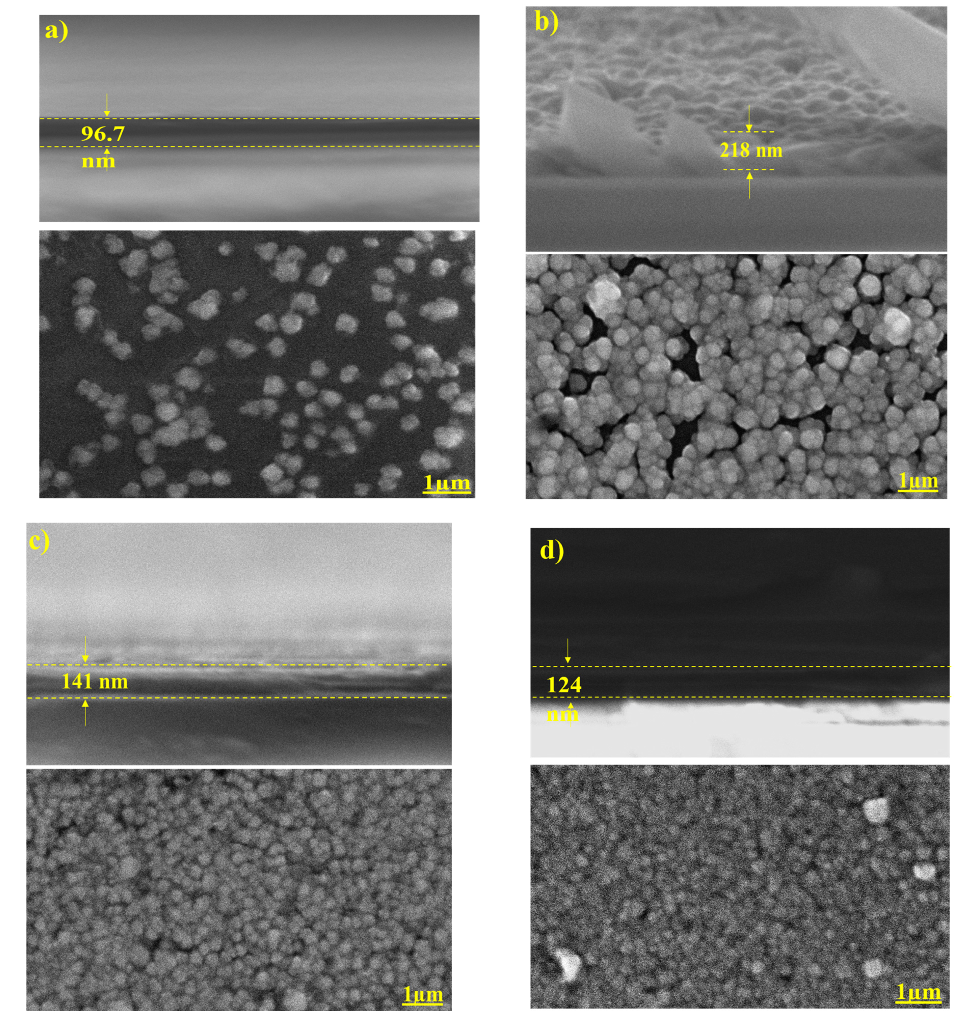
The morphology of the films could have a direct influence on the samples’ electrical and optical characteristics [55]. These micrographs illustrate that the resulting film has high coverage and less pinholes or cracks. As thiourea concentration is altered from 0.0015 M to 0.05 M, the grain size increased, and it can be seen from Figure 7 of the sample. At low S2− concentration, i.e., in the [1/0.75] sample, there is no cluster forming, and the deposited surface is smoother and more uniform compared with other samples due to the sulphur deficiency. Coupling this finding with the achieved XRD result, it can be concluded that no significant CdS deposition has happened compared with other samples, because of the quantity of CdS does not enough to detect by XRD, suggesting that film growth has started with the adsorption of small CdS particles on the substrate [56]. Additionally, the cross-section image for sample [1/0.75] in Figure 7a shows film thickness of 96.7 nm, which comes from unreacted cadmium and sulphur. Additionally, the rate of ion adsorption is related to the molar concentration of the precursor, and it is therefore difficult for ions with low molar concentrations to be adequately absorbed by the substrate in significant amounts [57].
Films are filled with spherical grains, the scale of which reduces, and their density rises significantly as [Cd]/[S] rises. In [1/1] sample, the fine particles collect and represent the full surface substrate continuously contributing to an inhomogeneous layer (Figure 7b). This may be due to the simultaneous occurrence of both the ion-by-ion mechanism and the cluster-by-cluster mechanism on the surface of the substrate [9]. Small clusters are agglomerate into larger particles discreetly scattered through the films due to increase in the ion-by-ion mechanism over cluster-by-cluster mechanism, as shown in Figure 7c for [1/5] ratio. This agrees with Zhao et al., who investigated the formation of CdS thin films by CBD and discovered that for S/Cd molar ratios of [5/1] and [9/1], grain size increases with dense film and no defined grain boundaries [47]. At [1/25] sample, higher charging negative has been occurred due to binding of sulphur ions in large quantities within the solution, which leads to insulation of the clusters, then accordingly increased electrostatic repulsion. This repulsion led to decreased particles size as well as arranged on the substrate surface in a regular manner with the great excess of sulphur ions [58].
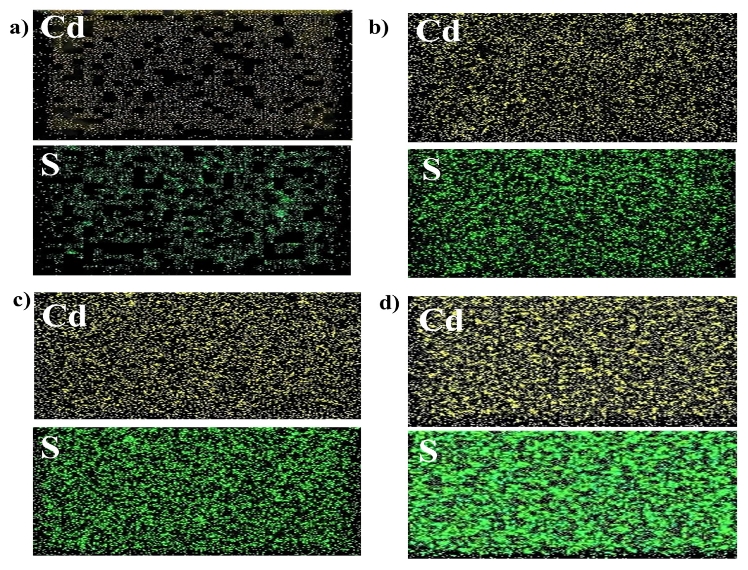
In material characterization, it is important to determine how the element is distributed laterally. This is achieved by using EDX mapping, which showed that the elemental distribution enhances with increasing the quantity of sulphur, Figure 8.
Moreover, the EDX spectrum confirms that the Cd and S atoms are presented in all the samples. Additionally, Figure 9 showed that the atomic percentage of sulphur in the whole thin films rises once further thiourea is incorporated into the bath. Simultaneously, [Cd/S] ratio gradually diminishes with increasing molar ratio up to [1/25].
It may thus be deduced that the percentage of sulphur in CdS rises and the total formation of clusters of CdS on the surface of glass rises with the increasing sulphur precursor.

3.4. Electrical Measurements

Due to the essential relationship between the optical and physical properties of the films, the impact of this interaction on the electrical characterizations of semiconductors is investigated in this section. The key electrical properties of interest for semiconductor materials are resistivity, mobility, and carrier concentration, which has been obtained using Hall Effect measurement and presented in Table 5 [59].
[1/1] sample showed the highest value of carrier concentration and lower resistivity. It is possible that, in this case, both Cd2+ and S2− in CdS lattice structure decreases the number of sites where grain boundary dispersion occurs. This is supported by both the lattice strain and the Urbach energy, as both of them are smaller than other samples. Cruz and colleagues revealed that reducing the [Cd]/[S] ratio significantly reduced the resistivity of the films, whilst more increments in the molar ratio led to increase the resistivity of the thin films [60]. The findings for both ratios at [1/5] and [1/25] are also in agreement with these findings. This might be related to insufficient incorporation of Cd and S into the lattice, most likely owing to the precursors’ low solubility in the growth solution. Based upon the analysis of the electrical properties of the samples in this current work, [1/1] samples have good electrical properties, so it will be more favourable for buffer layer solar cells compared to other ratios.

3.5. Mechanism

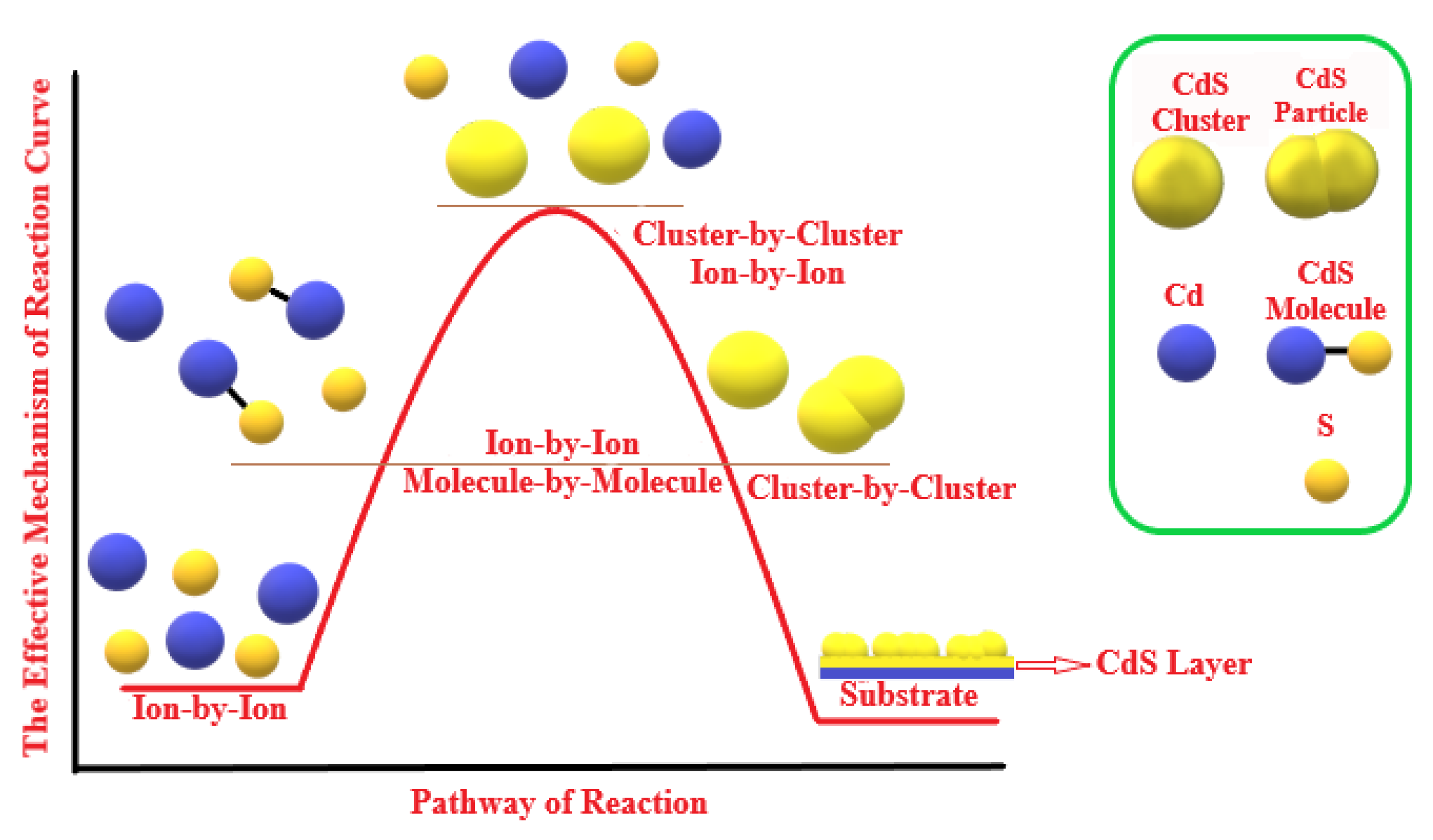
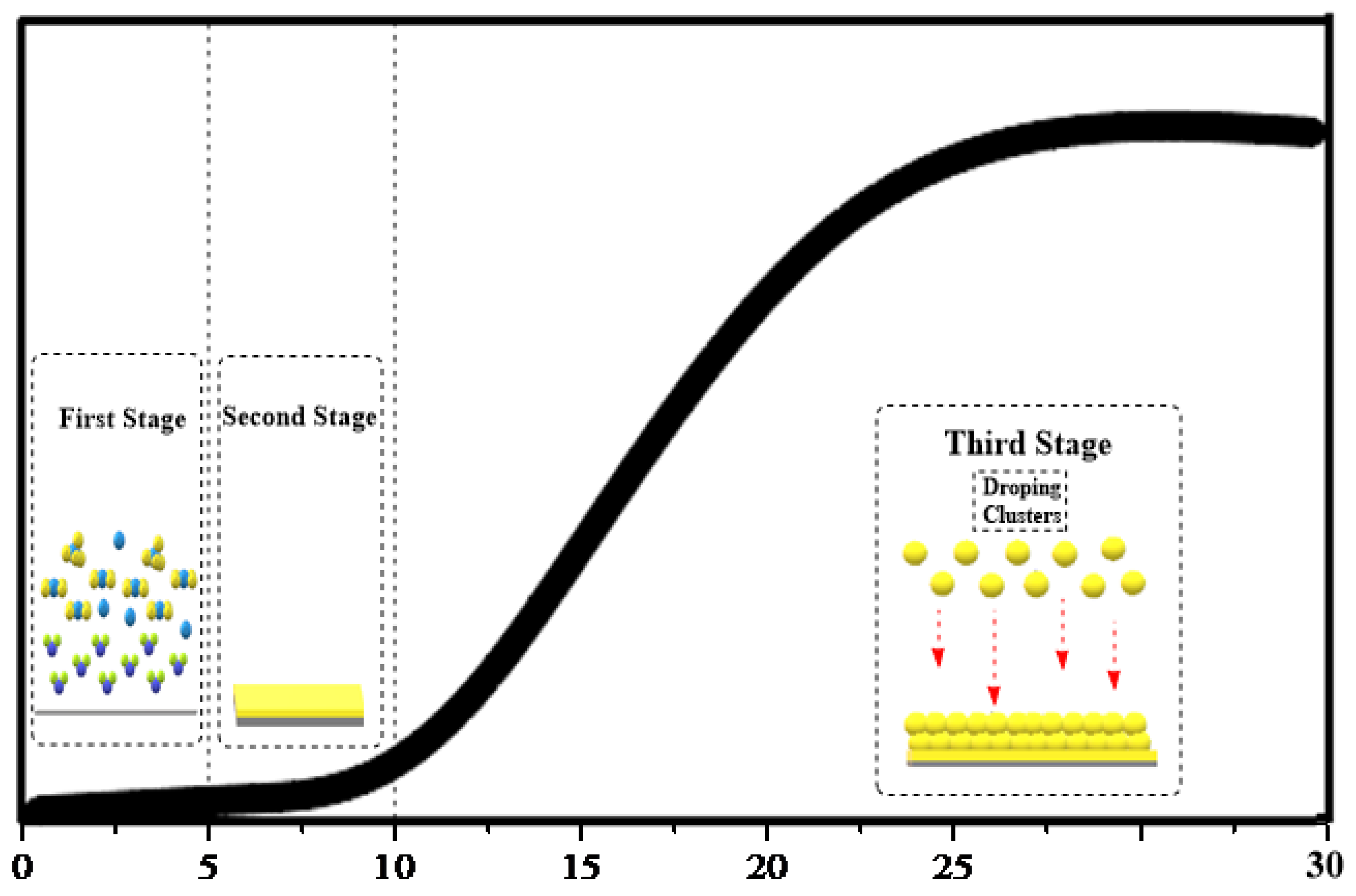
Chemical deposition of CdS films requires careful consideration of the growth mechanisms. Despite large number of publications of CdS films deposited by CBD, only limited studies connect the parameters of growth and consequent film characteristics to the CBD growth mechanisms. These previous literatures suggested mechanisms for CdS growth such as ion-by-ion, molecule-by-molecule, and cluster-by-cluster mechanisms [61,62,63,64]. These three mechanisms were frequently proposed by researchers who have worked on CBD method to prepare CdS films. Moreover, they have identified the intermediate compounds formed during the reaction as well as the end products. In order to detect whether these mechanisms cause CdS growth at random or predictable order, we proposed them occurring sequentially and simultaneously, as shown in the hypothetical curve of Figure 10.
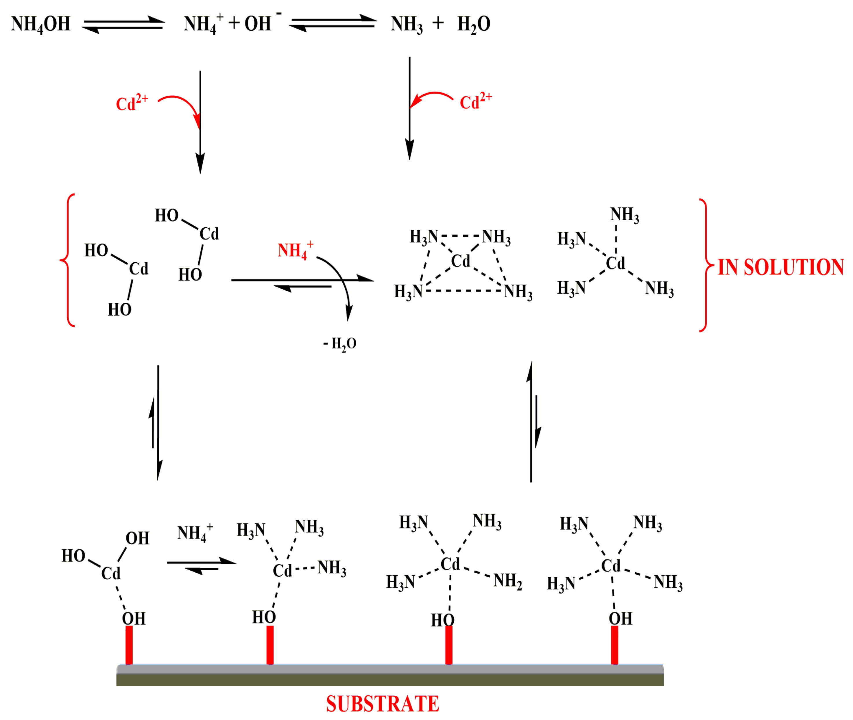
The mechanism begins with the formation of cadmium intermediate complexes and ends with stable intermediate complexes. Initially, the aqueous solution of ammonia with DI water was inside a beaker. Then, cadmium salt was added to the solution with stirring. In that moment, ammonia molecules were dissociating and released to attack the Cd2+ cations and formed both tetrahedral and square planar of tetraamine cadmium (II) ion [Cd(NH3)4]2+ as an intermediate. Meanwhile, another unstable intermediate complex (Cd(OH)2) has been formed, which is in equilibrium state with tetraamine cadmium (II) ion [Cd(NH3)4]2+ and quickly decomposed into [Cd(NH3)4]2+ complex again. The substrate surface has been affected by the adsorption of these two intermediates by the hydroxyl group of the substrate surface, which was attached to these two intermediates as depicted in Figure 11.
When thiourea solution was added to the reaction mixture, it was decomposed to release S2− sulphur ions. The number of anions was moderately and homogeneously distributed in the reaction solution and approached to the substrate surface to form hydrogen bonding with the hydroxyl groups S2−----H-O. At this stage, the ion-by-ion mechanism was started directly with the dissociation of the thiourea. Sulphur anions attack cadmium cations to form CdS molecules which distributed in the solution and precipitated on the substrate surface. The particles were arranged and separated from each other in a way that reduced the electrostatic repulsion and the steric effects among molecules. This arrangement is capable of enhancing the crystallinity and the cubic phase. Moreover, it is responsible for the formation of the first layer on the substrate surface and controls the path of the reaction [65,66,67]. After specific time, the CdS molecules and [Cd(NH3)4]2+ intermediate complexes began to collide with each other and molecule-by-molecule mechanism was started at this point to form cluster nuclei. In this case, the ion-by-ion mechanism was continued but at a smaller rate than in the starting of the reaction, i.e., the two mechanisms worked together with ion-by-ion and molecule-by-molecule mechanisms. Furthermore, most of the cations and anions were consumed by molecule-by-molecule mechanisms at the peak of the curve, as shown in Figure 10.
The possibility of ions colliding with each other becomes lower and the molecule-by-molecule mechanism becomes hard to occur due to the particles’ tendency to combine with each other to form cluster nuclei rather than molecules and third growth mechanism start. During this mechanism, CdS clusters were deposited on top of the first compact CdS film accompanied by slight ion-by-ion mechanism (due to lack of ions in the reaction vessel) until the end of the reaction. These sequences have been inferred from both of the experimental results as well as previous studies [68,69,70]. The duration of each growth stage depends on the chemical path parameters, which are: pH of solution, reagents concentration, growth times, and path temperature [71,72,73]. Therefore, changing growth parameters in CBD process gives very beneficial information to control the properties of deposited films. In this work, one of these parameters is the concentration of sulphur ion. Other factors, such as the concentration of cadmium ions, the pH of the reaction solution, and the reaction temperature, have been modified. The practical results showed that changing the sulphur ion concentration modified the CdS growth mechanism, which had an impact on the distribution of both cadmium and sulphur ions in the CdS crystal lattice, its form, and its arrangement on the substrate surface.
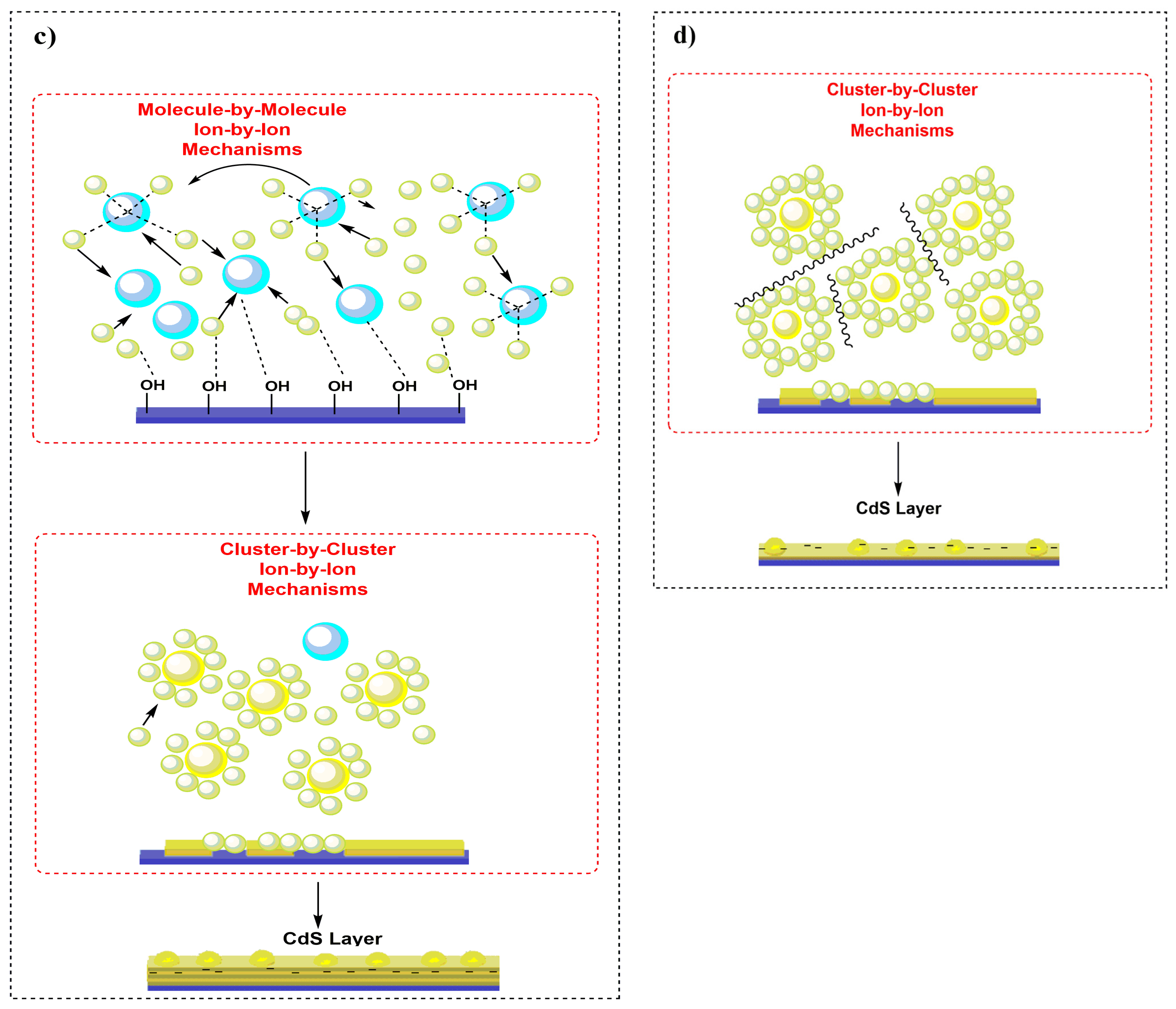
In the case of low concentration of thiourea [1/0.75], there is no sufficient quantity of sulphur ion to form CdS. At this concentration, the ion-by-ion action takes a short time due to the rapid penetration of sulphur ions, resulting in no CdS molecules being formed in the solution, Figure 12a. This is agreed with XRD results, Figure 3a. The diffractogram indicated that some of the Sulphur and Cd did not react and appeared as peaks at 2θ = 22.2°. The peak at 2θ = 22.2° was matched to Orthorhombic Sulphur (JCPDS-03-065-1436) with a preferred orientation along the (220) plane. This deterioration of CdS crystallinity appeared due to two reasons. Firstly, the decreased sulphur content in the precursor solution, and secondly, the surface adsorption of the intermediate complexes [Cd(NH3)4]2+ and Cd(OH)2 which formed in the solution.
When the concentration of sulphur ions was increased to equal the amount of cadmium ions [1/1], the ion-by-ion and cluster-by-cluster mechanisms were predominant, while the molecule-by-molecule mechanism was very fast, Figure 12b. This is owing to a random collision of particles and clusters on substrate surface which in turn leads to decrease the effect of the ion-by-ion mechanism on the surface. On the contrary, cluster-by-cluster mechanism is largely responsible to form the CdS surface which is approximately equals to the ions’ concentration by having a surface filled with cadmium and sulphur atoms [74]. If we matching this fact with Urbach energy, the lowest value is attribution to [1/1], as it is known to be higher in value in the samples with low crystalline, disorderly, and amorphous substances, since they have localized states which extended in the bandgap [52]. In addition to that, XRD results revealed that the concentration of sulphur ions in the solution affects the composition of the CdS film. Peak width (FWHM) calculations for concentrations [1/1] were the smallest possible: 0.325°. Thus, CdS film with [1/1] ratio had less amorphous phase than other concentrations.
In case of [1/5] concentration, the possibility of molecule-by-molecule mechanism increases, and the clusters are formed in large quantities due to increase the possibility of anions to collide with cadmium ions in the solution. It is worth noting that the surface of the substrate is completely layered as this was proved by the XRD results, which showed higher intensity pattern due to significant surrounding of sulphur ions around intermediate complexes [Cd(NH3)4]2+ and regular deposition of CdS. According to the proposed mechanism in Figure 12c, the amount of released sulphur ions leads to form small clusters and these clusters were shielded by Cd2+ ions. Thus, isolated CdS clusters by electrostatic repulsion will form small particles. This ion-by-ion mechanism will fill spaces on the surface of the substrate with excess sulphur ions, causing the CdS surface to be negatively charged which leads to create an unstable surface. In order to obtain a more stable surface, the molecule-by-molecule mechanism is preferable. This arrangement will encourage the formation of hexagonal phase, particularly when the molecule-by-molecule mechanism has been predominant. This matches with XRD results as it is able to be realized, and there is a slight shift in the dominant peak for [1/5] ratio, indicating a hexagonal phase.
Indeed, with increasing the thiourea concentration to high concentration [1/25], the deposited CdS on the substrate will change as well. When sulphur concentration is significantly increased, the randomness of the reaction is increased as well. This results in a large accumulation of negative charge on the surface of the CdS film that led to increase in the repulsion between the CdS particles that were deposited on the surface of the film and prevented formation of more particles. The XRD results agree with the SEM surface shapes and cross-sections of the three CdS films. The cross-sectional SEM images for each case revealed that the thickness of the CdS film decreased as the concentration of sulphur ions increased. It is attributed to the fact that the grain will be deposited on the substrate surrounded by a large number of sulphur ions, its contact will be weak because the binding forces to it are weak, and it will be easy to remove it only by washing with deionized water. As a result, the thickness of [1/1] was 218 nm, and the resulting layers were caused by equal concentrations of cadmium and sulphur ions, allowing the three mechanisms (ion-by-ion, molecule-by-molecule, and cluster-by-cluster mechanisms) to work gradually and consistently. The film thicknesses in the [1/5] and [1/25] cases were 141 nm and 124 nm, respectively.
The deposition rate increases with increasing bath temperature and deposition time, indicating a significant relationship between temperature and time with the growth rate [75]. When the sulphur ion concentrations changed, the temperatures and time used to grow the CdS films remained constant in all four cases. As Ashok et al. (2020) showed, at lower temperatures, the liberation of cadmium and sulphur ions will be less when using 65 °C and dominated by the ion-by-ion reaction mechanism, whereas the liberation of sulphur and cadmium ions will be higher at 80 °C [76].
As the deposition time increases, Figure 13 depicts the typical CBD growth curve. Using the quartz crystal microbalance (QCM) curve, Voss et al. (2004) identified three regimes of CdS layers film with increasing deposition time from 1 min to 30 min [77]. At the first, which is an induction regime, reaction rates are slow and deposits are not clearly visible. The onset of nucleation occurs during this period, which is characterized by rapid reaction times. The ions begin to be liberated from the initial structure of the reactants as the reaction begins, accompanied by a number of collisions of the ions liberated from the free cadmium and sulphur ions, forming the ion-by-ion mechanism. This stage is short stage in comparison to the third stage, which are (0–5) min. The molecular heterogeneous surface reactions-based compact layer growth regime is the second. During the initial stages of growth, the process exhibits a linear variation, and any small deviation from this pattern can be attributed to a period of coalescence. This stage creates the first layers of the CdS film, which are smooth, homogeneous, and free of pores. Because this stage is the initiator of the sedimentation process, the deposition time begins for 5 min after the reaction time. The second regime lasts approximately 5 to 10 min [76,78]. The growth regime for the porous layer is the third. Growth of a porous layer can be observed as the reaction time gradually increases, resulting in a noticeable increase in growth rate. Due to the formation of homogeneous particles that settle and adhere to the substrate, this layer has a porous appearance. The third stage has a time rate of (10–30) min, and it forms a cluster-by-cluster mechanism on the surface of the substrate [65].
One of the most important factors influencing CdS preparation and precipitation is pH. Previous research in this area was extensive. A decrease in the pH of the reaction system causes an increase in the concentration of free cadmium ions within the solution [79]. The CdS preparation reaction system’s basic media is critical for the formation of intermediate complexes required for the formation of the CdS film. The pH range most suitable for preparing these CdS films was 9 to 11, giving a majority for the cubic geometry of the crystal structure. An increase in pH above 12 reduces the crystallinity of the CdS film and results in an amorphous CdS film [80]. Cadmium intermediates formed prior to combining with sulphur ions are critical in preparing a homogeneous CdS film with higher crystallinity. Cd(OH)2, (square planar and tetrahedral) of [Cd(NH3)]42+, [Cd(OH)2SC(NH2)2]ads, and [(NH3)3Cd--]2+--OH-Site are an important intermediate compound formed during the preparation of CdS film when using NH4OH for setting the pH system of the reaction.
The absorbance and optical properties of the formed CdS films are calculated using the deposition mechanism of the interacting ions and the clusters formed inside the solution, as well as the clusters that grow on the substrate’s surface. In comparison to cases [1/5] and [1/25], case [1/1] has the highest absorbance. It has also been observed that the absorption edge moves down in energy as the film thickens and increases. The evolution of this change is associated with the fact that grain size grows in tandem with film thickness [81]. This increase in sulphur concentration is accompanied by a decrease in the bandgap, in addition to defects in the crystal lattice. That has led to the fact that the difference in the electrical properties of the formed films is explained by the optical properties and the CdS deposition mechanism. Excess sulphur ions at the surface and within the crystal lattice (which causes defects within the crystal lattice) will increase the electronic density, which is followed by high resistance (at case [1/5] and [1/25]). At [1/1], the carrier concentration has been increased owing to an enhance in the electron density, due to improvements in the electron–hole inside the crystal lattice.

3.6. The Influence of [Cd/S] Ratio on Cell Performance

To further demonstrate the viability of CdS thin film formation as a buffer layer, in this work we performed a numerical simulation to confirm experimental findings and to monitor the performance of enhanced CdS thin films on selected samples. To confirm the experimental finding, we employed the well-established CIGS (Mo/CIGS/CdS/ZnO) solar cell structure and the (Cd/S) experimental results for [1/1], [1/5], and [1/25] as a, b, and c, respectively. We ignore [1/0.75] due to low CdS deposited on the substrate, which also has been very clear in terms of XRD and optical properties.
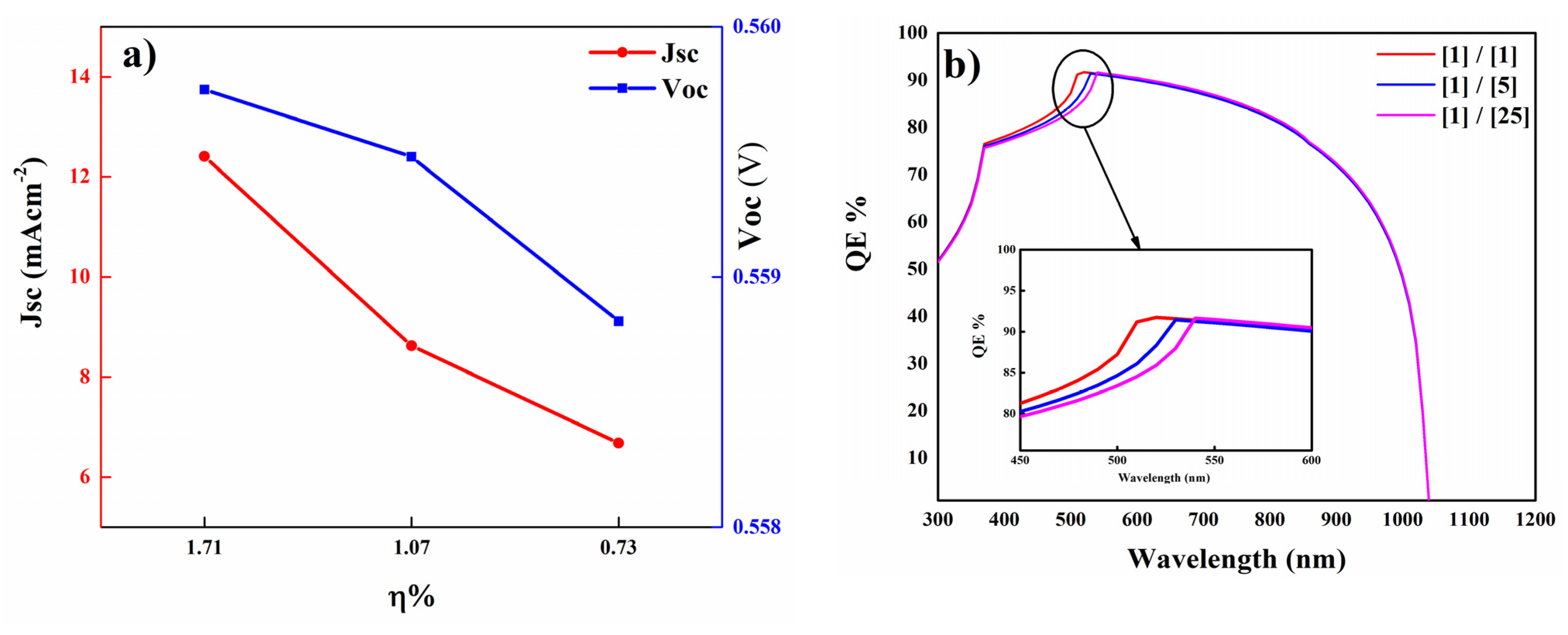
Furthermore, as seen in Table 6, the simulation findings indicate that the performance of CdS achieved at samples b and c is not optimal for solar cell applications, as the simulation indicates that there is a decrease in JSC and VOC with increasing sulphur content. A high conduction band offset (CBO) barrier can be overcome owing to the positive synergistic effects of a typical bandgap. Figure 14a shows that for all ratios examined, CdS at [1/1] had the best photovoltaic performance parameters. Moreover, the fill factor follows the open circuit voltage trend. Additionally, we noticed an increase in efficiency for CdS thin films with a 1/1 ratio, reaching 1.71%. While the CdS buffer layer-based solar cells have a high ratio, their efficiency is reduced to reach 0.73%.
However, sample a, with a response of around 91%, has the highest carrier collecting efficiency, showing less photocurrent interface recombination, Figure 14b. It is because these buffer layers are efficient at capturing photons. Thus, both experimental findings are valid and may be used to practically fabricate CIGS solar cells. Due to the fact that experimental results indicate that CdS with a 1/1 ratio has improved film characteristics, this research recommends using CdS with this ratio as a buffer layer for photovoltaic applications.

4. Conclusions

The influence of the sulphur precursor concentration on the optical, structural, morphological, and electrical properties of a CdS thin film has been examined. The expected CdS thin film growth mechanisms thru CBD process were also elucidated. Control of the reaction mechanism is important, as the change in the concentration of thiourea led to a change in most of the reaction properties and mechanisms responsible for the formation of the final product. XRD analysis of the CdS films showed a strong peak corresponding to (002) and (111) planes with both hexagonal and cubic structures, except at [1/0.75] ratio. There are no distinct peaks for CdS due to an insufficient amount of sulphur in CdS lattice to complete the formation. Optical analysis revealed that the (Cd: S) ratio affects the transparency of the film. Surface morphology showed that grains were randomly orientated on the surface, while it became more compact with increasing the sulphur concentration. Furthermore, the electrical data demonstrated that sample with [Cd]/[S] = 1 ratio exhibited the highest carrier concentration (3.21 × 1014 cm−3) and lowest resistivity (1843.9 Ω-cm). Finally, a numerical simulation involving the films’ optoelectronic properties was used to obtain the optimal conditions for the formation of CdS films. According to the modelling findings, the optimal concentration for fabricating the CdS buffer layer in CIGS solar cells is [1/1].

Author Contributions

Conceptualization, A.S.N.; methodology, A.S.N. and H.S.N.; software, D.A.R.M.A.; validation, A.S.N. and A.J.S.; formal analysis, H.M.; investigation, A.J.S.; resources, H.S.M.; data curation, S.A.H.; writing—original draft preparation, A.S.N.; writing—review and editing, H.A.H. and H.J.A.-I.; visualization, B.B.; supervision, K.S. and B.B.; project administration, K.S.; funding acquisition, A.A. All authors have read and agreed to the published version of the manuscript.

Funding

This research received no external funding.

Institutional Review Board Statement

Not applicable.

Informed Consent Statement

Not applicable.

Data Availability Statement

The study did not report any data.

Acknowledgments

The authors would like acknowledge the Universiti Kebangsaan Malaysia (UKM). The authors also would like to acknowledge both University of Technology-Iraq and Al-Mustaqbal University College, Babylon–Iraq.

Conflicts of Interest

The authors declare no conflict of interest.

References

  1. Sabbir, E.; Chelvanathan, P.; Ahmad, S.; Bais, B.; Kiong, S.; Sopian, K. Fabrication of Cu2SnS3 thin film solar cells by sulphurization of sequentially sputtered Sn/CuSn metallic stacked precursors. Sol. Energy 2019, 177, 262–273. [Google Scholar]
  2. Lv, B.; Yan, B.; Cai, P.; Li, Y.; Gao, F.; Ye, Z.; Lu, Z.; Sui, C.; Huang, P. Improving the structural and optical properties of CdS films grown by Chemical Bath Deposition with adding H2O2. Mater. Lett. 2018, 225, 42–45. [Google Scholar] [CrossRef]
  3. Willars-Rodríguez, F.J.; Chávez-Urbiola, I.R.; Hernández-Landaverde, M.A.; Vorobiev, P.; Ramírez-Bon, R.; Vorobiev, Y.V. Effects of tin-doping on cadmium sulfide (CdS:Sn) thin-films grown by light-assisted chemical bath deposition process for solar photovoltaic cell. Thin Solid Film. 2018, 653, 341–349. [Google Scholar] [CrossRef]
  4. Lu, Z.; Jin, R.; Liu, Y.; Guo, L.; Liu, X.; Liu, J.; Cheng, K.; Du, Z. Optimization of chemical bath deposited cadmium sulfide buffer layer for high-efficient CIGS thin film solar cells. Mater. Lett. 2017, 204, 53–56. [Google Scholar] [CrossRef]
  5. Swathi, S.; Yuvakkumar, R.; Ravi, G.; Babu, E.S.; Velauthapillai, D.; Syed, A.; Dawoud, T.M.S. Silver-doped cadmium sulfide for electrochemical water oxidation. Appl. Nanosci. 2020, 10, 4351–4358. [Google Scholar] [CrossRef]
  6. Mehmood, I.; Huang, J.; Khan, S.A.; Shah, A.H.; Khan, Q.U.; Kiani, M.; Zhou, D.; Li, G. Investigation of silver doped CdS co-sensitized TiO2/CISe/Ag–CdS heterostructure for improved optoelectronic properties. Opt. Mater. 2020, 111, 110645. [Google Scholar] [CrossRef]
  7. Zia, R.; Riaz, M.; Anjum, S. Study the effect of thiourea concentration on optical and structural properties of CdS-nanocrystalline thin films prepared by CBD technique. Optik 2016, 127, 5407–5412. [Google Scholar] [CrossRef]
  8. Beggas, A.; Benhaoua, B.; Attaf, A.; Aida, M.S. Growth study of CdS thin films deposited by chemical bath. Optik 2016, 127, 8423–8430. [Google Scholar] [CrossRef]
  9. Samir, P.; Raval, K. Investigation of structural, morphological and optical properties of cadmium sulphide (CdS) thin films at different Cd/S concentration deposited by chemical technique. J. Mater. Sci. Mater. Electron. 2017, 28, 18031–18039. [Google Scholar]
  10. Kwon, J.; Ahn, J.; Yang, H. Chemical bath deposition of CdS channel layer for fabrication of low temperature-processed thin-film-transistors. Curr. Appl. Phys. 2013, 13, 84–89. [Google Scholar] [CrossRef]
  11. Aliyu, M.; Diso, D.G.; Musa, A.O.; Abubakar, A.I. Effect of growth voltage on electrodeposited CdS thin films. Bayero J. Pure Appl. Sci. 2022, 13, 539–545. [Google Scholar]
  12. Shanmugapriya, S.; Sakthivel, B.; Nandhabalaji, S. ZnSe/CdS Thin Films Prepared with Physical Vapour Deposition Technique. ADALYA J. 2020, 9, 635–640. [Google Scholar]
  13. Shaikh, S.S.; Shkir, M.; Masumdar, E.U. Facile fabrication and characterization of modified spray deposited cadmium sulphide thin films. Phys. B Condens. Matter 2019, 571, 64–70. [Google Scholar] [CrossRef]
  14. Holi, A.M.; Al-Zahrani, A.A.; Najm, A.S.; Chelvanathan, P.; Amin, N. PbS/CdS/ZnO Nanowire Arrays: Synthesis, Structural, Optical, Electrical, and Photoelectrochemical Properties. Chem. Phys. Lett. 2020, 750, 137486. [Google Scholar] [CrossRef]
  15. Najm, A.S.; Chowdhury, M.S.; Munna, F.T.; Chelvanathan, P.; Selvanathan, V.; Aminuzzaman, M.; Techato, K.; Amin, N.; Akhtaruzzaman, M.D. Impact of cadmium salt concentration on cds nanoparticles synthesized by chemical precipitation method. Chalcogenide Lett. 2020, 17, 537–547. [Google Scholar]
  16. Najm, A.S.; Chelvanathan, P.; Tiong, S.K.; Ferdaous, M.T. Numerical insights into the influence of electrical properties of n-CdS buffer layer on the performance of SLG/Mo/p-absorber/n-CdS/n-ZnO/Ag configured thin film photovoltaic devices. Coating 2021, 11, 52. [Google Scholar] [CrossRef]
  17. Yılmaz, S.; Ünverdi, A.; Tomakin, M.; Polat, I.; Bacaksız, E. Surface modification of CBD-grown CdS thin films for hybrid solar cell applications. Optik 2019, 185, 256–263. [Google Scholar] [CrossRef]
  18. Nieto-Zepeda, K.E.; Guillén-Cervantes, A.; Rodríguez-Rosales, K.; Santos-Cruz, J.; Santos-Cruz, D. Effect of the sulfur and fluorine concentration on physical properties of CdS films grown by chemical bath deposition. Results Phys. 2017, 7, 1971–1975. [Google Scholar] [CrossRef]
  19. Kamble, A.; Sinha, B.; Agawane, G.; Vanalakar, S.; Kim, I.; Kim, J.Y.; Kale, S.S.; Patil, P.; Kim, J.H. Sulfur ion concentration dependent morphological evolution of CdS thin films and its subsequent effect on photo-electrochemical performance. Phys. Chem. Chem. Phys. 2016, 18, 28024–28032. [Google Scholar] [CrossRef]
  20. Chen, F.; Jie, W.; Cai, X. Effects of supersaturation on CdS film growth from dilute solutions on glass substrate in chemical bath deposition process. Thin Solid Film. 2008, 516, 2823–2828. [Google Scholar] [CrossRef]
  21. Azmi, N.; Chelvanathan, P.; Yusoff, Y.; Shahahmadi, S.A.; Tiong, S.K.; Sopian, K.; Amin, N. A comprehensive study on the effects of alternative sulphur precursor on the material properties of chemical bath deposited CdS thin films. Ceram. Int. 2020, 46, 18716–18724. [Google Scholar] [CrossRef]
  22. Munna, F.; Chelvanathan, P.; Sobayel, K.; Nurhafiza, K.; Sarkar, D.; Nour, M.; Sindi, H.; Rawa, M.; Sopian, K.; Amin, N.; et al. Effect of zinc doping on the optoelectronic properties of cadmium sulphide (CdS) thin films deposited by chemical bath deposition by utilising an alternative sulphur precursor. Optik 2020, 218, 165197. [Google Scholar] [CrossRef]
  23. Hsu, W.-T.; Chiang, C.-C.; Yeh, T.-K.; Lan, C.-W.; Tsai, S.-Y. CdS Thin Film Prepared by Shallow Chemical Bath Deposition for Low Cost CIGS Thin Film Solar Cell. In Proceedings of the 2011 37th IEEE Photovoltaic Specialists Conference, Seattle, WA, USA, 19–24 June 2011; pp. 2723–2726. [Google Scholar]
  24. Kaur, I.; Pandya, D.K.; Chopra, K.L.; Soc, J.E. Growth Kinetics and Polymorphism of Chemically Deposited CdS Films Growth Kinetics and Polymorphism of Chemically Deposited CdS Films. J. Electrochem. Soc. 1980, 127, 943–948. [Google Scholar] [CrossRef]
  25. Sengupta, S.; Aggarwal, R.; Raula, M. A review on chemical bath deposition of metal chalcogenide thin films for heterojunction solar cells. J. Mater. Res. 2022, 1–12. [Google Scholar] [CrossRef]
  26. Jadhav, U.S.; Kale, S.S.; Lokhande, C.D. Effect of Cd: S ratio on the photoconducting properties of chemically deposited CdS films. Mater. Chem. Phys. 2001, 69, 125–132. [Google Scholar] [CrossRef]
  27. Xiao, Q.; Xiao, C. Surface-defect-states photoluminescence in CdS nanocrystals prepared by one-step aqueous synthesis method. Appl. Surf. Sci. 2009, 255, 7111–7114. [Google Scholar] [CrossRef]
  28. Yuan, X.; Li, M.; Ruan, H.; Yang, Y.; Liu, Y.; Zhang, L. CdS nanoparticles with high photocatalytic property synthesized by a new liquid—Liquid method. J. Mater. Sci. Mater. Electron. 2016, 27, 6030–6034. [Google Scholar] [CrossRef]
  29. Kakhaki, Z.M.; Youzbashi, A.A.; Sangpour, P.; Naderi, N.; Orooji, Y. Influence of Cd salt concentration on the photoconductivity of CdS thin films prepared by chemical bath technique. Mater. Sci. Semicond. Process. 2022, 148, 106773. [Google Scholar] [CrossRef]
  30. Najm, A.S.; Naeem, H.S.; Alabboodi, K.O.; Hasbullah, S.A. New systematic study approach of green synthesis CdS thin film via Salvia dye. Sci. Rep. 2022, 12, 12521. [Google Scholar] [CrossRef]
  31. Burgelman, M.; Nollet, P.; Degrave, S. Modelling polycrystalline semiconductor solar cells. Thin Solid Film. 2000, 362, 527–532. [Google Scholar] [CrossRef]
  32. Jaymin, R.; Tapas, K.C.; Chetan, P.; Kinjal, P.; Keyur, P.; Gopal, B.; Priya, S. PbS-ZnO solar cell: A numerical simulation. J. Nano-Electron. Phys. 2017, 9, 03041. [Google Scholar]
  33. Chelvanathan, P.; Istiaque, M.; Amin, N. Performance analysis of copper–indium–gallium–diselenide (CIGS) solar cells with various buffer layers by SCAPS. Curr. Appl. Phys. J. 2010, 10, 387–391. [Google Scholar] [CrossRef]
  34. Akter, F.; Mohammad, J.; Rashid, J. Simulation study to find suitable dopants of CdS buffer layer for CZTS solar cell. J. Theor. Appl. Phys. 2020, 14, 75–84. [Google Scholar]
  35. Najm, A.S.; Moria, H.; Ludin, N.A. Areca catechu as photovoltaic sensitizer for dye-sensitized solar cell (DSSC). Biointerface Res. Appl. Chem. 2020, 10, 5636–5639. [Google Scholar]
  36. Nakanishi, T.; Ito, K. Properties of chemical bath deposited CdS thin films. Sol. Energy Mater. Sol. Cells 1994, 35, 171–178. [Google Scholar] [CrossRef]
  37. Alexander, J.N.; Higashiya, S.; Caskey, D.; Efstathiadis, H. Deposition and characterization of cadmium sulfide (CdS) by chemical bath deposition using an alternative chemistry cadmium precursor. Sol. Energy Mater. Sol. Cells 2014, 125, 47–53. [Google Scholar] [CrossRef]
  38. Graf, A.; Maticiuc, N.; Spalatu, N.; Mikli, V.; Mere, A.; Gavrilov, A.; Hiie, J. Electrical characterization of annealed chemical-bath-deposited CdS fi lms and their application in superstrate con fi guration CdTe/CdS solar cells. Thin Solid Film. 2014, 582, 351–355. [Google Scholar] [CrossRef]
  39. Subba, K.; Pilkington, R.D.; Hill, A.E.; Tomlinson, R.D.; Bhatnagar, A.K. Structural and optical investigations on CdS thin films grown by chemical bath technique. Mater. Chem. Phys. 2001, 68, 22–30. [Google Scholar] [CrossRef]
  40. Ahmed, N.M.; Sulaiman, N.H.; Abdullah, M.F.; Najm, A.S.; Afzal, N.; Altowyan, A.S.; Rafique, M. Improvement in structural, optical and electrical properties of ito film through aln and HfO2 buffer layers. Surf. Rev. Lett. 2021, 28, 2150094. [Google Scholar] [CrossRef]
  41. Munna, F.; Selvanathan, V.; Sobayel, K.; Muhammad, G.; Asim, N.; Amin, N.; Sopian, K.; Akhtaruzzaman, M. Diluted chemical bath deposition of CdZnS as prospective buffer layer in CIGS solar cell. Ceram. Int. 2020, 47, 11003–11009. [Google Scholar] [CrossRef]
  42. Mohammadi, B.; Yousefi, A.A.; Bellah, S.M. Effect of tensile strain rate and elongation on crystalline structure and piezoelectric properties of PVDF thin films. Polym. Test. 2007, 26, 42–50. [Google Scholar] [CrossRef]
  43. Pandya, S.G. Preparation and Characterization of Cadmium Sulphide Nanocrystalline Thin Film Grown by Chemical Method. Int. J. Recent Sci. Res. 2016, 7, 14887–14890. Available online: http://www.recentscientific.com (accessed on 1 January 2020).
  44. Öztas, M.; Bedir, M.; Öztürk, Z.; Korkmaz, D.; Sur, S. Structural and Optical Properties of Nanocrystal In2O3 Films by Thermal Oxidation of In2S3 Films. Chin. Phys. Lett. 2006, 23, 1610. [Google Scholar] [CrossRef]
  45. Najm, A.S.; Mohamad, A.B.; Ludin, N.A. The extraction and absorption study of natural dye from Areca catechu for dye sensitized solar cell application. Am. Inst. Phys. 2017, 1838, 020019. [Google Scholar]
  46. Zanatta, A.R. Revisiting the optical bandgap of semiconductors and the proposal of a unified methodology to its determination. Sci. Rep. 2019, 9, 11225. [Google Scholar] [CrossRef] [PubMed]
  47. Zhao, X.H.; Wei, A.X.; Zhao, Y.; Liu, J. Structural and optical properties of CdS thin films prepared by chemical bath deposition at different ammonia concentration and S/Cd molar ratios. J. Mater. Sci. Mater. Electron. 2013, 24, 457–462. [Google Scholar] [CrossRef]
  48. Ouachtari, F.; Rmili, A.; Elidrissi, B.; Bouaoud, A.; Erguig, H.; Elies, P. Influence of Bath Temperature, Deposition Time and S/Cd Ratio on the Structure, Surface Morphology, Chemical Composition and Optical Properties of CdS Thin Films Elaborated by Chemical Bath Deposition. J. Mod. Phys. 2011, 2, 1073–1082. [Google Scholar] [CrossRef]
  49. Najm, A.S.; Ludin, N.A.; Abdullah, M.F.; Almessiere, M.A.; Ahmed, N.M.; Al-Alwani, M.A.M. Areca catechu extracted natural new sensitizer for dye-sensitized solar cell: Performance evaluation. J. Mater. Sci. Mater. Electron. 2020, 31, 3564–3575. [Google Scholar] [CrossRef]
  50. Najm, A.S.; Ludin, N.A.; Hamid, N.H.; Ibrahim, M.A.; Teridi, M.A.M.; Sopian, K.; Moria, H.; Holi, A.M.; Al-Zahrani, A.A.; Naeem, H.S. Effect of Chenodeoxycholic Acid on the Performance of Dye-sensitized Solar Cells utilizing Pinang Palm (Areca catechu) Dye. Sains Malays. 2020, 49, 2971–2982. [Google Scholar] [CrossRef]
  51. Hassanien, A.S.; Akl, A.A. Effect of Se addition on optical and electrical properties of chalcogenide CdSSe thin films Superlattices and Microstructures Effect of Se addition on optical and electrical properties of chalcogenide CdSSe thin films. Superlattices Microstruct. 2016, 89, 153–169. [Google Scholar] [CrossRef]
  52. Ikhmayies, S.; Ahmad-Bitar, R.N. Temperature dependence of the photoluminescence spectra of CdS: In thin fi lms prepared by the spray pyrolysis technique. J. Lumin. 2013, 142, 40–47. [Google Scholar] [CrossRef]
  53. Ikhmayies, S.J.; Ahmad-Bitar, R.N. Thickness Dependence of the Bandgap Energy and Urbach Tail for CdS Thin Films Prepared by Vacuum Evaporation. Proc. Elev. World Renew. Energy Congr. Exhib. 2010, 979–984. [Google Scholar]
  54. Faris Abdullah, M.; Zulkifli, R.; Moria, H.; Soheil Najm, A.; Harun, Z.; Abdullah, S.; Wan Ghopa, W.A.; Sulaiman, N.H. Assessment of TiO2 Nanoconcentration and Twin Impingement Jet of Heat Transfer Enhancement—A Statistical Approach Using Response Surface Methodology. Energies 2021, 14, 595. [Google Scholar] [CrossRef]
  55. Faris Abdullah, M.; Zulkifli, R.; Harun, Z.; Abdullah, S.; Wan Ghopa, W.A.; Soheil Najm, A.; Humam Sulaiman, N. Impact of the TiO2 nanosolution concentration on heat transfer enhancement of the twin impingement jet of a heated aluminum plate. Micromachines 2019, 10, 176. [Google Scholar] [CrossRef]
  56. Carreón-Moncada, L.; González, A.; Rodríguez-Galicia, J.L.; Rendón-Angeles, J.C. Chemical deposition of CdS films by an ammonia-free process with amino acids as complexing agents. Thin Solid Film. 2016, 599, 166–173. [Google Scholar] [CrossRef]
  57. Ashith, V.; Rao, G.K. Bandgap tailoring in CdxZn1−xS alloy films deposited by successive ionic layer adsorption and reaction. Thin Solid Film. 2017, 626, 1–8. [Google Scholar]
  58. Yilmaz, S.; Tomakin, M.; Unverdi, A.; Aboghalon, A. A Study on Hydrothermal Grown CdS Nanospheres: Effects of Cd/S Molar Ratio. J. Sci. 2019, 32, 1271–1281. [Google Scholar] [CrossRef]
  59. Al-Sajad, G.A.; Holi, A.M.; L-Zahrani, A.A.A.; Najm, A.S. Titania Nanotubes Arrays Based-Gas Sensor: NO2-Oxidizing Gas and H2 Reducing Gas. Nano Biomed. Eng. 2020, 12, 191–196. [Google Scholar] [CrossRef]
  60. Cruz, J.S.; Pérez, R.C.; Delgado, G.T.; Angel, O.Z. CdS thin films doped with metal-organic salts using chemical bath deposition. Thin Solid Film. 2010, 518, 1791–1795. [Google Scholar] [CrossRef]
  61. Hop, B.X.; van Trinh, H.; Dat, K.Q.; Bao, P.Q. Growth o f CdS thin films by chemical bath deposition technique. J. Sci. Math. 2008, 24, 119–123. [Google Scholar]
  62. Kim, M.J.; Kim, H.T.; Kang, J.K.; Kim, D.H. Molecular Crystals and Liquid Crystals Effects of the Surface Roughness on Optical Properties of CdS Thin Films. Mol. Cryst. Liq. Cryst. 2010, 532, 437–444. [Google Scholar] [CrossRef]
  63. Mohammed, I.M.S.; Gubari, G.M.M.; Huse, N.P.; Dive, A.S.; Han, S.H. Effect of Cd/S ratio on growth and physical properties of CdS thin films for photosensor application. J. Mater. Sci. Mater. Electron. 2020, 31, 9989–9996. [Google Scholar] [CrossRef]
  64. Mugdur, P.H.; Chang, Y.J.; Su, Y.W.; Morrone, A.A.; Ryu, S.O.; Lee, T.J.; Chang, C.H. A Comparison of Chemical Bath Deposition of CdS from a Batch Reactor and a Continuous-Flow Microreactor. J. Electrochem. Soc. 2007, 154, D482. [Google Scholar] [CrossRef]
  65. Ouafi, M.; Jaber, B.; Atourki, L.; Zayyoun, N.; Ihlal, A.; Mzerd, A.; Laânab, L. In Situ Low-Temperature Chemical Bath Deposition of CdS Thin Films without Thickness Limitation: Structural and Optical Properties. Int. J. Photoenergy 2018, 2018, 4549154. [Google Scholar] [CrossRef]
  66. Djelloul, A.; Adnane, M.; Larbah, Y.; Zerdali, M.; Zegadi, C.; Messaoud, A. Effect of Annealing on the Properties of Nanocrystalline CdS Thin Films Prepared by CBD Method. J. Nano-Electron. Phys. 2016, 8, 02005–1–02005-7. [Google Scholar] [CrossRef]
  67. Senthil, K.; Mangalaraj, D.; Narayandass, S.K. Structural and optical properties of CdS thin Flms. Appl. Surf. Sci. 2001, 170, 476–479. [Google Scholar] [CrossRef]
  68. Slonopas, A.; Ryan, H.; Foley, B.; Sun, Z.; Sun, K.; Globus, T.; Norris, P. Growth mechanisms and their effects on the opto-electrical properties of CdS thin fi lms prepared by chemical bath deposition. Mater. Sci. Semicond. Process. 2016, 52, 24–31. [Google Scholar] [CrossRef]
  69. Sandoval-paz, M.G.; Ramírez-bon, R. Analysis of the early growth mechanisms during the chemical deposition of CdS thin fi lms by spectroscopic ellipsometry. Thin Solid Film. 2009, 517, 6747–6752. [Google Scholar] [CrossRef]
  70. Choi, C.; Paul, B.K.; Chang, C. Microreactor-Assisted Solution Deposition for Compound Semiconductor Thin Films. Processes 2014, 2, 441–465. [Google Scholar] [CrossRef]
  71. Challa, K.K.; Magnone, E.; Kim, E.T. Highly photosensitive properties of CdS thin films doped with boron in high doping levels. Mater. Lett. 2012, 85, 135–137. [Google Scholar] [CrossRef]
  72. Daniel-Umeri, R.A. Effect of pH on the Optical Properties of Cadmium Sulphide (CdS) Thin Film Deposited Using Chemical Bath Method. Int. J. Mater. Sci. Appl. 2015, 4, 138–142. [Google Scholar] [CrossRef]
  73. Pawar, S.M.; Pawar, B.S.; Kim, J.H.; Joo, O.; Lokhande, C.D. Recent status of chemical bath deposited metal chalcogenide and metal oxide thin fi lms. Curr. Appl. Phys. 2011, 11, 117–161. [Google Scholar] [CrossRef]
  74. Singaevsky, A.F.; Piryatinski, Y.; Grynko, D.O.; Dimitriev, O.P. Asymmetric effect of (000 1 - ) and (0001) facets on surface and interface properties of CdS single crystal. Appl. Phys. A 2011, 104, 493–502. [Google Scholar]
  75. Dhere, N.G.; Waterhouse, D.L.; Sundaram, K.B.; Melendez, O.; Parikh, N.R.; Patnaik, B. Studies on chemical bath deposited cadmium sulphide films by buffer solution technique. J. Mater. Sci. Mater. Electron. 1995, 6, 52–59. [Google Scholar] [CrossRef]
  76. Regmi, A.A.G.; Núñez, A.R.; López, M.S.; Castaneda, H. Comparative studies of CdS thin films by chemical bath deposition techniques as a buffer layer for solar cell applications. J. Mater. Sci. Mater. Electron. 2020, 31, 7499–7518. [Google Scholar]
  77. Voss, C.; Subramanian, S.; Ryu, S.O. Growth Kinetics of Thin-Film Cadmium Sulfide by Ammonia-Thiourea Based CBD. J. Electrochem. Soc. 2014, 151, 8–13. [Google Scholar] [CrossRef]
  78. Zhang, L.; Jiang, J.; Wang, W.; Huang, X.; Yuan, Q.; Hong, R.; Cha, L. Growth process and properties of CdS thin films prepared by chemical bath deposition at different pH values. J. Mater. Sci. Mater. Electron. 2018, 29, 7637–7643. [Google Scholar] [CrossRef]
  79. Hodes, G. Chemical Solution Deposition of Semiconductor Films; CRC Press: Boca Raton, FL, USA, 2002. [Google Scholar]
  80. Kariper, A.; Güneri, E.M.; Göde, F.; Gümüş, C.E. Effect of pH on the physical properties of CdS thin films deposited by CBD. Chalcogenide Lett. 2012, 9, 27–40. [Google Scholar]
  81. Ikhmayies, S.J. A Study of the Absorption Edge of ZnO Thin Films Prepared by the Spray Pyrolysis Method. Miner. Met. Mater. Ser. 2018, 8, 83–92. [Google Scholar]
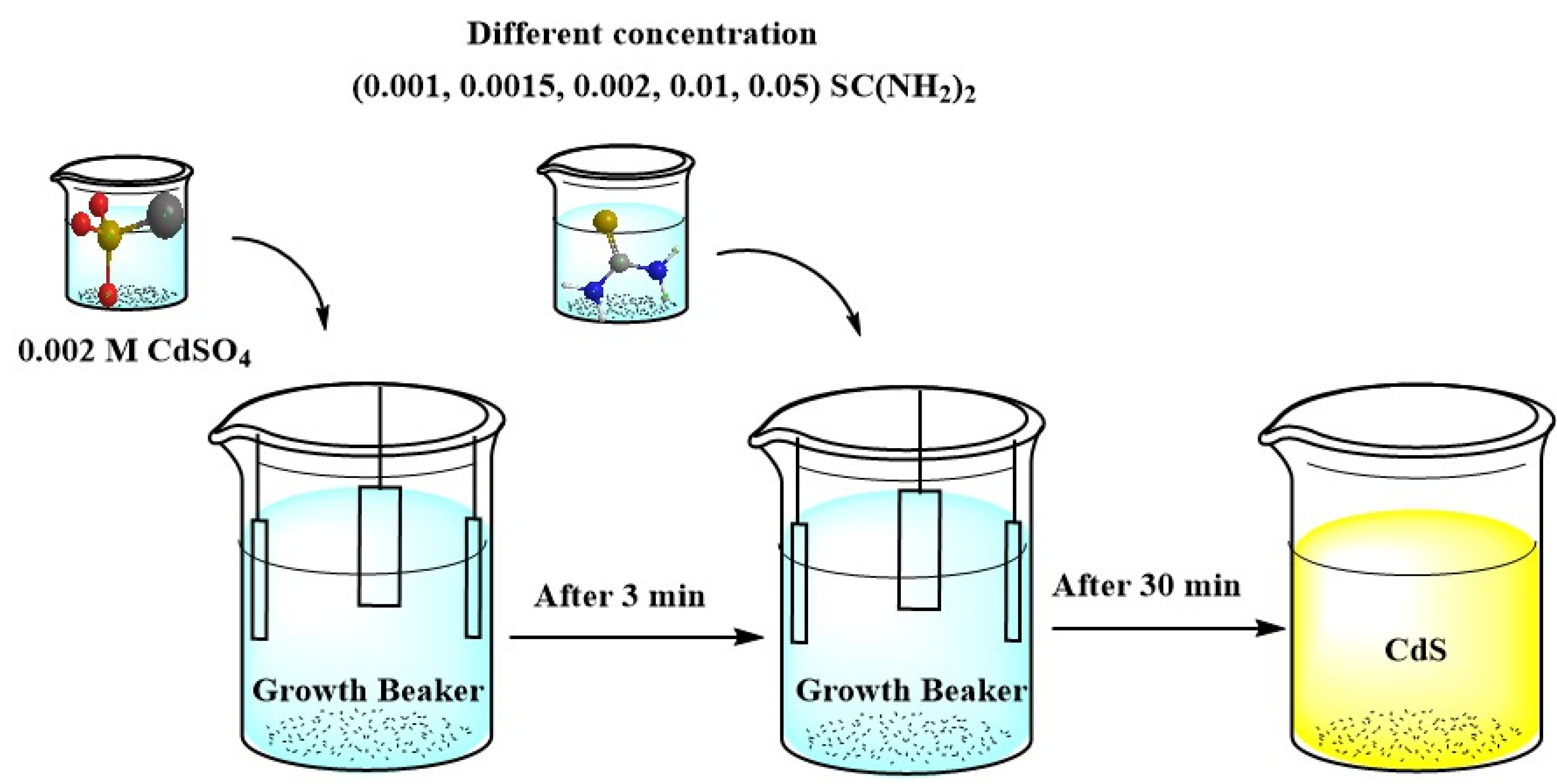
Figure 1. Synthesis CdS thin film by CBD technique.
Coatings 12 01400 g001
Figure 2. Device configuration for CIGS solar cell.
Coatings 12 01400 g002
Figure 3. (a) XRD for [Cd]/[S] ratios, (b) FWHM, Lattice strain, crystalline size vis [Cd]/[S] molar ratio.
Coatings 12 01400 g003
Figure 4. (a) Influence of [Cd]/[S] ratio on the absorbance of CdS thin films, (b) Difference of (αhν)2 with photon energy ().
Coatings 12 01400 g004
Figure 5. Urbach energy of Cd/S films.
Coatings 12 01400 g005
Figure 6. The difference of bandgap and Urbach energy-based molar concentration.
Coatings 12 01400 g006
Figure 7. SEM micrograph of CdS thin film at; (a) [1/0.75], (b) [1/1], (c) [1/5], (d) [1/25].
Coatings 12 01400 g007
Figure 8. EDX elemental mapping of CdS thin film for different (Cd/S) ratio as (a) [1/0.75], (b) [1/1], (c) [1/5], (d) [1/25].
Coatings 12 01400 g008
Figure 9. Atomic% of cadmium and sulphur for different [Cd/S] ratio.
Coatings 12 01400 g009
Figure 10. Curve of path of the CdS thin film mechanism.
Coatings 12 01400 g010
Figure 11. The formation of intermediate cadmium complexes and their connections.
Coatings 12 01400 g011
Figure 12. The formation of CdS for: (a) [1/0.75], (b) [1/1], (c) [1/5], and (d) [1/25].
Coatings 12 01400 g012aCoatings 12 01400 g012b
Figure 13. The typical growth curve and growth mechanism of a CBD-based film.
Coatings 12 01400 g013
Figure 14. CIGS solar cells with different Cd/S ratio at; (a) Photovoltaic performance parameters, (b) QE%.
Coatings 12 01400 g014
Table 1. Chemical reagents used in CBD process.
PurposeChemicalQuantity
StabilizerDIW water360 mL
Cadmium sourceCdSO40.002 m
Sulphur sourceSC(NH2)2 0.001–0.05 m
Buffer Solution and pH ControlNH4OH3.5 m (40 mL)
Table 2. Summary of physical and electrical characteristics for each layer parameter [32,33,34].
Layers’ Characteristicsn-ZnOn-CdS (1/1)n-CdS (1/5)n-CdS (1/25)p-CIGS
Layer thickness (nm)801001001001000
Dielectric constant, εr1010101010
Electron mobility, µn (cm²/V·s)50ExperimentExperimentExperiment50
Hole mobility, µp (cm²/V·s)2020202020
Acceptor concentration, NA (cm−3)00005.5 × 1015
Donor concentration, ND (cm−3)5 × 10¹⁷ExperimentExperimentExperiment0
Band gap, Eg (eV)3.4ExperimentExperimentExperiment1.2
Electron affinity, χ (eV)4.554.454.454.454.5
Conduction band density of states, NC (cm−3)4 × 10182 × 10182 × 10182 × 10182 × 1018
Valance band density of states, NV (cm−3)9 × 10181.5 × 10191.5 × 10191.5 × 10192 × 1018
Electron thermal velocity (cm s−1)1 × 1071 × 1071 × 1071 × 1071 × 107
Hole thermal velocity (cm s−1)1 × 1071 × 1071 × 1071 × 1071 × 107
Table 3. Defect properties.
Layers’ Characteristicsn-ZnOn-BufferCIGS
Defect TypeNeutralNeutralNeutral
Electron capture cross section (cm2)10−1210−1310−15
Hole capture cross section (cm2)10−1210−1310−13
Energetic distributionGauẞGauẞGauẞ
Reference for defect energy level EtAbove EvAbove EvAbove Ev
Energy level with respect to reference (eV)1.6501.200(0.6/1.1) × Eg-Absorber
Characteristic energy (eV)0.1000.1000.100
Total defect density, NT-total (cm−3)1.772 × 10161.772 × 1017(0–1.772) × 1017
Peak defect density NT-peak (eV−1·cm−3)1 × 10171 × 1018(0–1) × 1018
Table 4. CdS thin film structural parameters.
Sample Angle
(2θ Degree)
The Interplane
Spacing ‘d’ (nm)
FWHM ‘B
Peak Width (°)
Lattice Strain, ε (%)Crystallite
Size (nm) ‘D’
[1/1]27.23°0.3260.3250.58525.80
[1/5]27.06°0.3280.4700.85217.70
[1/25]27.20°0.3270.5761.03914.40
Table 5. Electrical properties for various CdS thin film molar ratio.
SampleResistivity, (Ω cm)Carrier Concentration, (1/cm3)Mobility, (cm2 Vs)Hall Coefficient (cm3/C)
[1]/[1]1843.93.210 × 101412.86−2.19 × 10⁴
[1]/[5]3937.11.406 × 101410.39−5.13 × 10⁴
[1]/[25]6595.12.199 × 101417.24−3.79 × 10⁴
Table 6. Performance of CIGS solar cells with various Thiourea concentrations.
Sample JSC (mA/cm2)VOC (V)FF (%)Efficiency (%)
[1/1]12.400.55924.711.71
[1/5]8.620.55922.321.07
[1/25]6.670.55819.610.73
Publisher’s Note: MDPI stays neutral with regard to jurisdictional claims in published maps and institutional affiliations.