Abstract
This study presents a multilayer design and fabrication of an optical notch filter for enhancing visual quality. A cost-effective multilayer design of notch filter with low surface roughness and low residual stress is proposed. A 9-layer notch filter composed of SiO2 and Nb2O5 with a central wavelength of 480 nm is prepared by electron beam evaporation combined with ion-assisted deposition. The optical transmittance, residual stress, and surface morphology are measured by a UV/VIS/NIR spectrophotometer, Twyman-Green interferometer and field emission scanning electron microscopy (FE-SEM). The transmittance of the notch filter at the central wavelength is above 15%, and the average transmittance of the transmission band is about 80%. The residual stress of the notch filter is −0.235 GPa, and the root mean square surface roughness is 1.85 nm. For improving the visual quality, a good image contrast can be obtained by observing the microscopic image using the proposed notch filter.
1. Introduction
Optical notch filters based on thin film coatings have many important applications. Such filters are usually used for the transmission of some wavelengths, and blocking and/or reflection of other wavelengths. In other words, the notch filter can selectively reflect a portion of the spectrum while transmitting all other wavelengths. In the related literature, the use of high-end multilayer film manufacturing technology includes the advanced-plasma-source (APS) assisted electron beam evaporation [1], plasma assisted reactive magnetron sputtering (PARMS) [2,3,4], HELIOS (Leybold Optics) magnetron sputtering [5,6], ion-assisted electron beam evaporation [7], etc. Among them, electron beam evaporation technology has the potential for industrialized mass production and application. Electron beam evaporation can produce significantly higher deposition rates and can be widely used for optical coatings such as high purity thin film and conductive glass. In addition, compared with other PVD processes, electron beam evaporation also has a very high material utilization efficiency, thereby reducing manufacturing costs. For instance, Zhang et al. [8] presented the design and production approach of an ultra-steep notch filter by ion-assisted electron-beam deposition. The constrained optimization method was used to design of the ultra-steep notch filter. As compared to the notch filter designs obtained by using apodization technique [9], some layers near the substrate were additionally optimized to suppress transmittance ripples in the passbands. With the help of these optical interference filters, scientists can more effectively evaluate the properties of materials by separating specific wavelengths of interest. On the other hand, optical image contrast plays an important role in determining the use of filters for visual application. Selecting the correct optical filters can improve the contrast of the captured image and reduce the processing time required to extract the relevant image data. The research challenge is how to produce these notch filters with high reproducibility, high layer quality, low surface roughness, reasonable film stress and cost effectiveness (low manufacturing costs).
As mentioned above, a notch filter is the opposite of a band-pass filter. It blocks the wavelength of one band and passes through longer and shorter wavelengths. Considering optical filters for eye care, the anti-blue light filter lens is a common case- since blue light is short-wavelength electromagnetic radiation (400–500 nm) in the visible spectrum (400–780 nm) that carries the highest amount of energy per photon. It has attracted more and more attention due to a hypothesis suggesting that blue light may cause photochemical damage to the retina [10,11,12,13,14]. Although too much blue light is theoretically harmful, adequate blue light is necessary for normal visual function. For example, blue light plays an important role in color discrimination [15] and night vision. One problem with the use of blue light filters as a protective measure against blue light hazards is that the peak sensitivity of night vision and melatonin suppression are in the blue-green and blue spectral ranges, respectively.
In the application of optoelectronic devices, the notch filter is an optical interference filter commonly used to control the transmission and reflection of light. The optical notch filter has a variety of functions; for example, it can be applied to projection displays, head-up displays (HUD) and various optical products [16,17]. For head-up displays, lasers or light-emitting diodes (LEDs) of specific wavelengths are generally used as light sources. The notch filters are designed to reflect or transmit a specific wavelength of light while transmitting/reflecting all other wavelengths outside the stop/passband. The HUD provides the ability to project information onto a transparent screen, making it look like a floating virtual image. Using the suitable optical devices, the virtual image is combined with the view of the real world seen through the screen, so that the two images appear to be at the same distance. In order to obtain sufficient reflection, optical thin films are deposited on the glass or plastic substrate surface to increase the reflectivity by optical interference effect.
It is difficult to design an optical notch filter by changing the traditional method of alternately stacking high refractive index and low refractive index layers- because the bandwidth of the rejection region is defined by the refractive index ratio of the materials constituting the coating. A narrow rejection band means a low refractive index ratio, and this in turn implies a large number of coating layers to obtain a significant rejection level. In 2006, Leitel et al. [1] reported that the graded-index layers and rugate structures were performed by coevaporation of silicon dioxide (SiO2) as the low index material and niobium pentoxide (Nb2O5) as the high index material. For the rugate structure, TEM cross-sectional investigations delivered good quality profiles. In 2014, Lyngnes and Kraus [18] presented an apodized thickness design method for discrete layer notch filters. They combined the relatively easy fabrication of discrete layer design with the low ripple design. The establishment of optimization function can optimize the design of a non-quarter wave film structure. In 2016, Hoggan et al. [19] designed an optical notch filter, with the centered wavelength at 480 nm to reduce direct stimulation of intrinsically photosensitive retinal ganglion cells. This notch filter could reduce headache impact in chronic migraine subjects. In 2019, Kumar et al. [20] reported a 44-layer reflective notch filter using an Al2O3/SiO2 multilayer structure. The multilayer structure was deposited on BK7 substrate using electron-beam and ion assisted deposition (IAD) techniques. The fabricated filter was characterized for its optical properties using a UV-Vis-NIR spectrophotometer. Kumar et al. [21] proposed the design and fabrication of a 44-layer optical reflective notch filter. The performance of the fabricated notch filter was studied at normal (0°) and oblique (45°) incidence angles. The thickness modulated reflective stack of the filter was designed by using the materials Al2O3 and SiO2. These research works can achieve good results. However, the use of two materials to make optical notch filters is not limited to the commonly used coating materials, SiO2, Al2O3 and TiO2. They did not address the issue of residual stress control and image contrast of the notch filters. In our previous work, a new laser protective lens based on a multilayered notch filter design with low residual stress and low surface roughness was presented [7]. An18-layer notch filter was prepared by an electron beam evaporation with ion-assisted deposition technique, which is composed of SiO2 and Nb2O5 with a center wavelength of 532 nm. The transmittance of the center wavelength is 0.2%, the bandwidth of the notch filter is about 100 nm, and the average transmittance of the transmission band is about 70%.
It is well known that amorphous silicon dioxide is most widely utilized as low refractive index material in optical coatings. It has a wide transmittance region from ultraviolet to mid−infrared with a refractive index of 1.46 and very small wavelength dispersion in the visible region. On the other hand, niobium pentoxide is used as a high refractive index material in optical coatings. The Nb2O5 thin film is stable and homogeneous by electron beam evaporation process, and its refractive index is 2.01. The morphology of the Nb2O5 thin film shows to be amorphous, similar to the low index layer of SiO2 thin film. The choice of the high refractive material Nb2O5 was stimulated by related research to deposit high quality Nb2O5 layers, using ion-assisted electron beam evaporation. Both films are amorphous and suitable for low loss optical coatings. Therefore, we designed and fabricated a cost-effective optical notch filter by using Nb2O5 and SiO2 thin film materials with a center wavelength of 480 nm to improve the visual quality of the observed microscopic images. Our multilayer notch filter design is not a band-stop filter. In the visual optics applications, its residual transmittance cannot be reduced too low. The specific visible light band is necessary to consider the color distortion of the eye vision. The proposed notch filter design refers to a FL-41 tinted lens [19], which can provide more benefits for human visual color saturation.
2. Materials and Methods
2.1. Thin Film Preparation
A cost-effective notch filter was designed by the optical thin film software of Essential Macleod [22]. The notch filter design was composed of alternately stacked low-refractive index (L) SiO2 and high-refractive index (H) Nb2O5 materials. The multilayered quarter-wave thick stack was designed in terms of an air/L(HL)4/substrate. Table 1 lists the design results of the 9-layer notch filter with a central wavelength of 480 nm. In the multilayered film deposition process, the dual electron beam evaporation system associated with ion-assisted deposition (IAD) technique is used. The electron beam evaporation coating system is described as follows: The vacuum system consists of an oil rotary pump (RP) and a mechanical booster pump. A diffusion pump was used for the fine pumping operation, and a helium cold trap (helium cold trap) captured water vapor in the form of helium condensation in an air compressor to help improve the efficiency of the vacuuming rate. The multilayer films were prepared by dual electron-beam evaporation with ion beam-assisted deposition. The vacuum chamber was evacuated to a base pressure of less than 2.7 × 10⁻⁴ Pa. Thin films were deposited on B270 glass (25 mm in diameter), BK7 glass lens (65 mm in diameter), and silicon wafer substrates. The coating substrates were cleaned by ultrasonication. Argon and oxygen gases (99.999% purity) were used in the coating process. During the thin film deposition, the maximum output power of the electron gun was 10 kW, the voltage was 10 kV, and the current was 1 A. The anode current of the ion source for ion-assisted deposition was 0.5~10 A, the anode voltage was 80~300 V, and the ion energy was 50–200 eV. The film thickness monitoring used quartz monitoring and optical monitoring methods, respectively. The quartz monitoring device adopted a 5 MHz quartz crystal oscillator; meanwhile the optical monitoring used a spectrometer with a wavelength range of 360–1000 nm and reflected the change in reflectance when the film was deposited on the glass substrates. The turning points of reflectivity were used to stop each thin film layer deposition process. The vacuum value of the coating process was below 6 × 10⁻⁴ Pa. The electron beam power during evaporation was 400 W for SiO2 and 4000 W for Nb2O5, respectively. The deposition rate was 0.4 nm/s for SiO2 and 0.1 nm/s for Nb2O5. The oxygen gas injected during the Nb2O5 layer deposition was 80 sccm. The film thickness correction factor (tooling value) is defined as the film thickness ratio between the optical monitor glass and the coating sample, which can be obtained through single-layer film deposition. The tooling values of SiO2 and Nb2O5 materials were 0.95 and 0.80, respectively. For the ion-assisted deposition, the argon flow rate was 16 sccm for the SiO2 layer and 10 sccm for the Nb2O5 layer. The anode voltage and anode current of the SiO2 film deposition were 130 V and 2 A; meanwhile, the anode voltage and anode current of the Nb2O5 film were 100 V and 2.5 A. During the multilayer coating process, the temperature of the different substrates was heated to 150 °C.

Table 1.
Notch filter design of B270/SiO2(Nb2O5/SiO2)4/air.
2.2. Thin Film Measurement
Different instruments are used to measure the optical transmittance, residual stress, surface roughness and microstructure characteristics of the notch filter after the coating process. The optical transmittance was measured by a Shimadzu UV-2600i spectrometer (Shimadzu, Kyoto, Japan) with a resolution of 0.1 nm and a wavelength range of 200–900 nm. In the residual film stress measurement, a self-developed Twyman−Green interferometer was used as the hardware architecture to measure the residual film stress [23]. A semiconductor laser beam is passed through a micro-objective and a pinhole which acts as a spatial filter to form a point source. This beam propagates through a collimating lens to form a plane wavefront. The wavefront is divided in amplitude by a beam splitter. The reflected and transmitted beams travel to a reference mirror and the tested glass substrate. The tested glass substrate is mounted on a three-axis platform to generate the spatial-carrier frequency and forms interference fringes. After being reflected by both the reference mirror and the substrate, the beams are recombined by the beam splitter and travel toward a digital CMOS camera (Basler, Ahrensburg, Germany). The camera has a resolution of 1920 × 1200 pixels. The interference pattern can be seen on the LCD monitor attached to the CMOS camera. The interferogram is recorded by a personal computer equipped with a self-developed MATLAB film stress analysis program.
The MATLAB program was developed by the fast Fourier transform (FFT) method [24]. The surface profile of the thin film can be reconstructed by the phase unwrapped method [25], and the radius of curvature of the tested substrate can be measured. Assuming that the residual stress is isotropic, the residual stress in a thin film deposited on a substrate results in substrate deformation proportional to the film stress. By measuring the radius of the curvature difference between the substrate before and after thin film deposition, the film stress can then be determined by using the modified Stoney’s formula [26].
where σf is the residual stress in thin films. tf is the total thickness of the thin films, R and R’ correspond to the radius of the curvature of the substrate measured before and after the multilayered thin film deposition. For a given substrate, Young’s modulus (Es), Poisson’s ratio (νs), and thickness (ts) are constants. By convention, σf is negative for compressive stress and positive for tensile stress. In other words, tensile stress is present in the film if the curvature of the substrate is concave; conversely, the stress is compressive if the curvature of the substrate is convex.
For the surface roughness measurement, a self-developed Linnik microscopic interferometer was used to measure the surface roughness of the thin film. A He−Ne laser with a wavelength of 632.8 nm is used as the light source. When the laser light passes through the spatial filter and the collimating lens, a parallel light is formed. A beam splitter divides the incident light into two parallel light beams. One beam strikes the reference mirror surface, and the other beam hits the surface of the tested sample after passing through the microscope objective lens. When the two beams are reflected separately and overlapped by the beam splitter, they are on the imaging plane. The interference fringes are captured by a high-resolution CCD camera (Allied Vision, Stadtroda, Germany), and then interferograms are analyzed by the self-developed MATLAB program. The analytical program mainly uses the fast Fourier transform method to obtain the change in height difference of the thin film surface. Secondly, a digital Gaussian filter is used to define the signal cut-off wavelength to separate the high-frequency roughness signal from the low-frequency surface profile. Finally, the 3D surface profile of the thin film can be reconstructed, and the surface roughness parameter values can be calculated through numerical analysis [27,28]. In order to verify the surface roughness, atomic force microscopy (AFM, Digital Instruments, Bresso, Italy) was used to measure and compare the surface roughness of the thin films.
For the microstructural analysis, the microstructure of thin films was observed by Hitachi S-4800 field emission scanning electron microscope (SEM, Hitachi High-Tech, Tokyo, Japan). The scanning electron microscope technique is one of the well-established instruments to investigate the surface microstructure of thin films. SEM produces images by probing the sample with a focused beam of electrons, which interacts with atoms on the surface to produce various signals that contain information about the material [29]. In this work, SEM photographs were taken at 1.00 µm fraction. The captured photographs were used for further analysis.
3. Results and Discussion
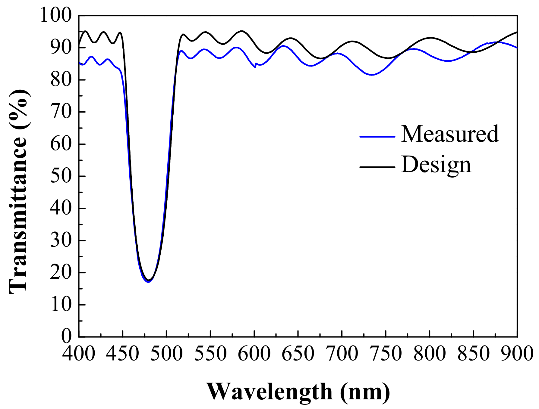
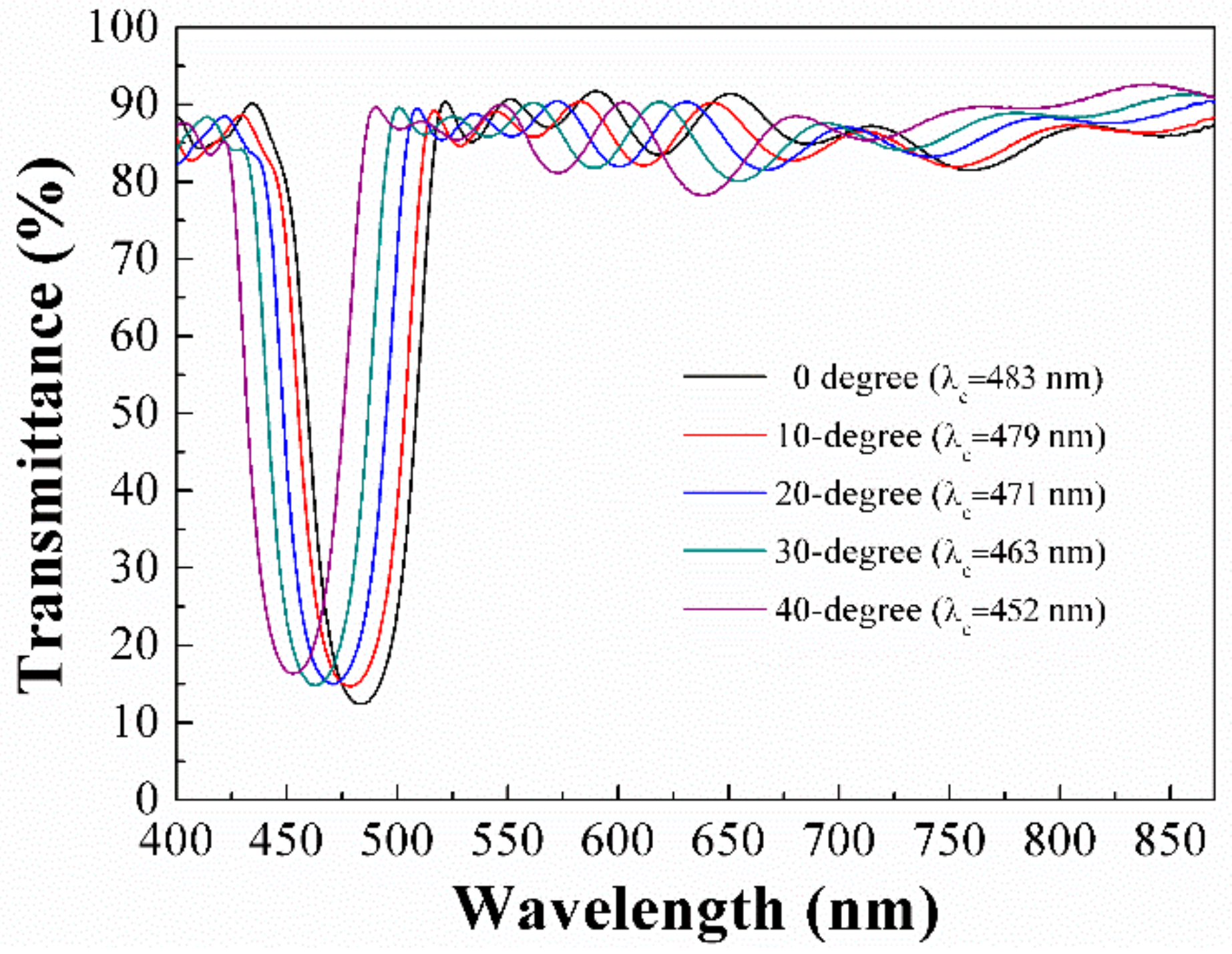
Figure 1 demonstrates the picture of the 480 nm notch filter spectacle lenses. The experimental measurement spectrum curve is compared with the result simulated by Essential Macleod software. Figure 2 shows the transmission spectra of the measured and design results of the 9-layer notch filter with a center wavelength of 480 nm. It can be seen that the center wavelength of the transmission spectrum, the transmittance of the notch band and the bandwidth of the notch filter are consistent with the design. As can be seen from Figure 2, the central wavelength difference between the design and experimental samples is 1 nm. The designed thickness of the notch filter is 2.371 μm, but the coating thickness of the manufactured notch filter is 2.125 μm, which is 0.146 μm thinner than the designed multilayer film. Therefore, compared with the designed spectral curve, the measured spectral curve of the coated sample shows a red shift from the change of the spectral curve. Furthermore, the notch band characteristics of the notch filter are very similar to the design results. The reason for the affected ripple of the transmission band is that the top layer of SiO2 film is closest to the air, so it is more sensitive to the change of transmission rate of the transmission band. Our notch filter is based on the optical multilayer interference effect, and its transmittance depends on the angle of incidence. As the incidence angle increases, the center wavelength of the notch filter shifts to a shorter wavelength. Figure 3 shows that as the incidence angle increases from 0° to 40°, the center wavelength of the proposed notch filter moves from 483 to 452 nm. The spectra reveal that the transmittance of the notch filter at oblique incidence (40°) angle has a peak shift of 31 nm toward the blue region corresponding to a central wavelength of ∼452 nm. It should be noted that there is no change in the performance of the side ripples outside the band. Furthermore, there is a 4% increment in the dip transmittance value for the incident light from normal incidence to 40 degrees. This decrease in reflection intensity and peak shift to the shorter wavelength side are due to the decrease in the optical path difference between the constituent light waves originating from the thin film interface of the multilayer stack. This result is consistent with the literature [21].
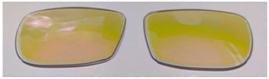
Figure 1.
The picture of the notch filter coated on spectacle lenses.
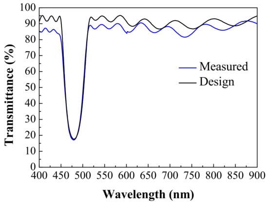
Figure 2.
Transmittance spectra of a 9-layer notch filter.
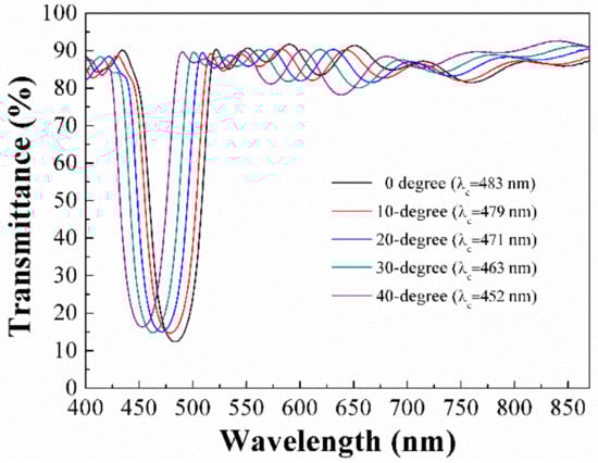
Figure 3.
Transmittance spectra of the notch filter measured by different incidence angles.
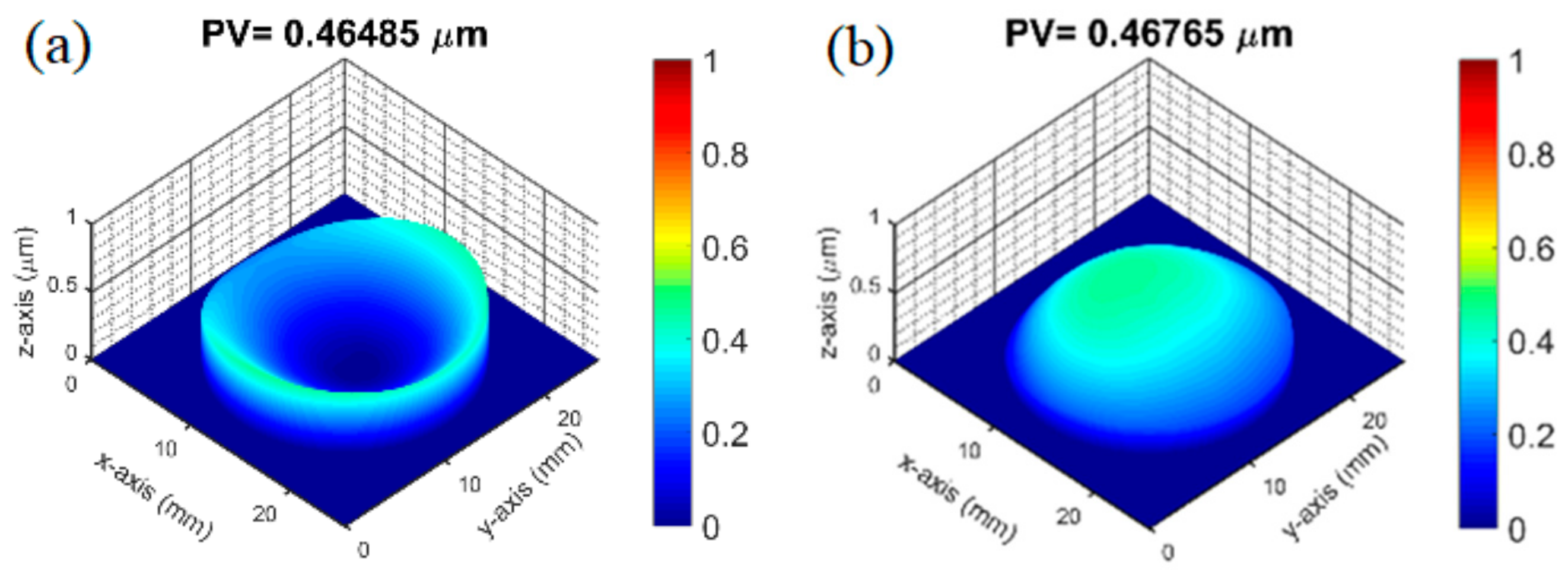
Figure 4 shows the results of wavefront sensing measurement on the left- and right-eye spectacle lenses. The notch filter was deposited on the spectacle lenses made of BK7 glass material. From the experimental results, the wavefront surface variation of the uncoated wavefront profile of the left- and right-eye spectacle lenses can be determined by the wavefront sensing measurement. The peak-valley (PV) values of the uncoated lenses are about 43.87 and 42.99 μm, and the radii of curvature of the left and right spectacle lenses are 4.09 and 4.23 m, respectively. The PV values of the wavefront surface after the multilayer coating of the notch filter are 30.07 and 28.02 μm, and the radii of curvature are 6.33 and 7.07 m, respectively. Obviously, the spectacle lenses will be affected by multilayer film deposition and change the wavefront surface profile.

Figure 4.
3-D surface contour of the B270 substrate (a) before coating; (b) after coating.
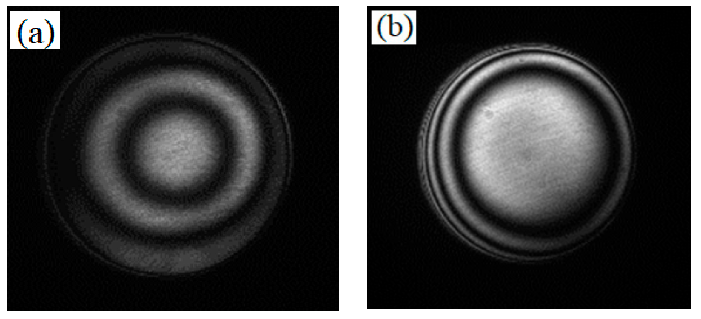
No matter what kind of thin film preparation technology is used, the thin film will produce residual stress in the growth process−because excessive residual stress levels can dramatically affect the performance, reliability, and durability of multilayer components and devices. As the residual tensile stress is too large, the thin film is easy to peel off or crack, and if the residual compressive stress is too large, the thin film may be wrinkled or broken. Therefore, the measurement of residual stress is one of the important mechanical properties of the multilayer films. For the residual stress measurement, a Tywman−Green interferometer was used to measure the radii of curvature before and after the 9-layer notch filter coated on the B270 glass (25.4 mm in diameter and 1.5 mm in thickness), and then the residual stress was calculated by the proposed method. Figure 5 discloses the interferogram of 9-layer notch filter before and after coating. The 3-D surface contour of the B270 glass substrate before and after coating is shown in Figure 5. The radius of curvature before coating is 120.335 ± 0.535 m, and the radius of curvature after multilayer coating is −188.867 ± 1.429 m. From the change of surface profile, it can be seen that the surface shape of the glass substrate is concave. After coating 9 layers notch filters, the surface shape becomes convex, and the residual stress is −0.259 GPa. The residual intrinsic stresses of single-layer SiO2, Nb2O5 film and multilayer notch filter are measured by the Twyman−Green interferometer, and the residual compressive stresses of single-layer SiO2, Nb2O5 film are −0.353 and −0.254 GPa. The residual compressive stress of the 9-layer optical notch filter is −0.235 GPa and the stress value is smaller than that of the SiO2 and Nb2O5 single layer. Compared with the single-layer film, the multi-layer film has a lower compressive stress, indicating that the source of stress contribution not only comes from the single-layer film, but may also derive from the interfacial stress and thermal stress. It can be seen from these results that the notch filter presents a low stress state.
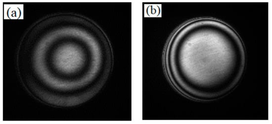
Figure 5.
Interferogram of 9-layer notch filter (a) substrate before coating; (b) substrate after coating.
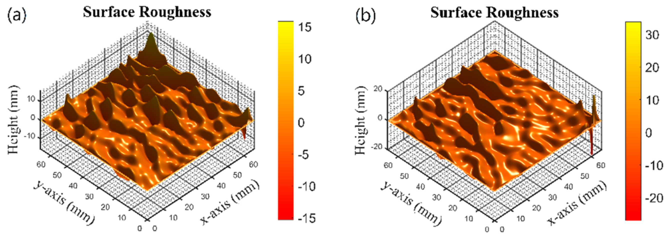
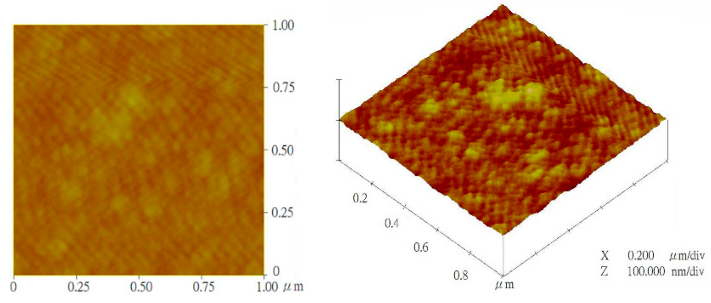
Thin film growth is a promising field in modern nanoscience. Surface roughness usually causes scattering of electrons or light [30]. Surface roughness is one of the film characteristics that need to be understood after thin film coating. The surface roughness will directly affect the amount of optical scattering, which will seriously reduce the transmittance of the filter, so a good optical interference filter has the characteristics of low surface roughness. Figure 6 shows the surface roughness of the notch filter by using a Linnik microscopic interferometer. The root mean square (RMS) surface roughness of B270 glass before coating is 2.18 nm, and the RMS surface roughness after multilayer coating is 1.85 nm. Atomic force microscopy (AFM) is a scanning probe microscopy technique with a resolution of 0.1 Å. AFM permits direct visualization of 3-D images of thin film topography. The RMS surface roughness measured by AFM is 2.177 nm, as shown in Figure 7. The AFM image shows the tiny columnar grains, and the collected data are analyzed in three dimensions. The surface roughness values measured by the two instruments are similar. After the multilayered notch filter is coated on B270 glass, the surface roughness decreases. The RMS surface roughness value of the notch filter measured by AFM is less than that measured by Linnik microscopic interferometer. These results show that the notch filter has a smooth surface and low surface roughness. When the measured values of the same sample are converted to RMS surface roughness, the results are usually different due to the different resolutions and bandwidth limitations of the instrument.

Figure 6.
Surface roughness of (a) substrate before coating; (b) substrate after multilayer coating.
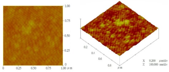
Figure 7.
Surface roughness of the notch filter measured by AFM.
In addition, from the transmittance spectrum, the difference between the designed value and the measured spectral transmittance is very small, so the measured surface roughness value will not seriously affect the transmittance of the notch filter. The multilayer coating surfaces can be imaged by scanning electron microscopy (SEM). Figure 8 shows the top view and cross-sectional micro-images of the multilayer stack coated with Nb2O5 and SiO2 by using the dual electron beam evaporation associated with the ion-assisted deposition technique. It is noted that the notch filter structure consists of 9 layers distributed uniformly throughout the surface of the substrate. This SEM micro-image reveals a dark to bright contrast that corresponds to the compositional profile of the thin film. The low- and high-index layers in the micrograph correspond to SiO2 and Nb2O5 thin films, respectively. The total thickness of the whole layer stack is about 2.37 µm. Some finer pores can be seen in SEM examination. The SEM micro-image indicates that the SiO2 film structure is continuous and dense. For the Nb2O5 thin film, a columnar structure is observed from the SEM micrograph, which is consistent with the measurement results of residual stress. The results reveal that the residual compressive stress of SiO2 thin film is larger than that of Nb2O5 thin film.
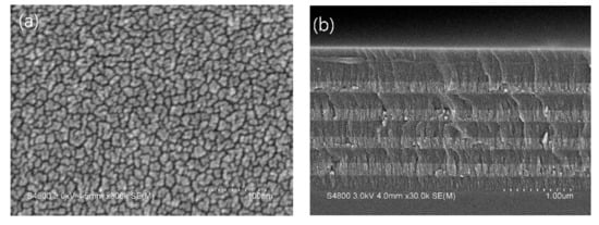
Figure 8.
SEM micro-images of multilayer notch filter (a) top view; (b) cross-section.
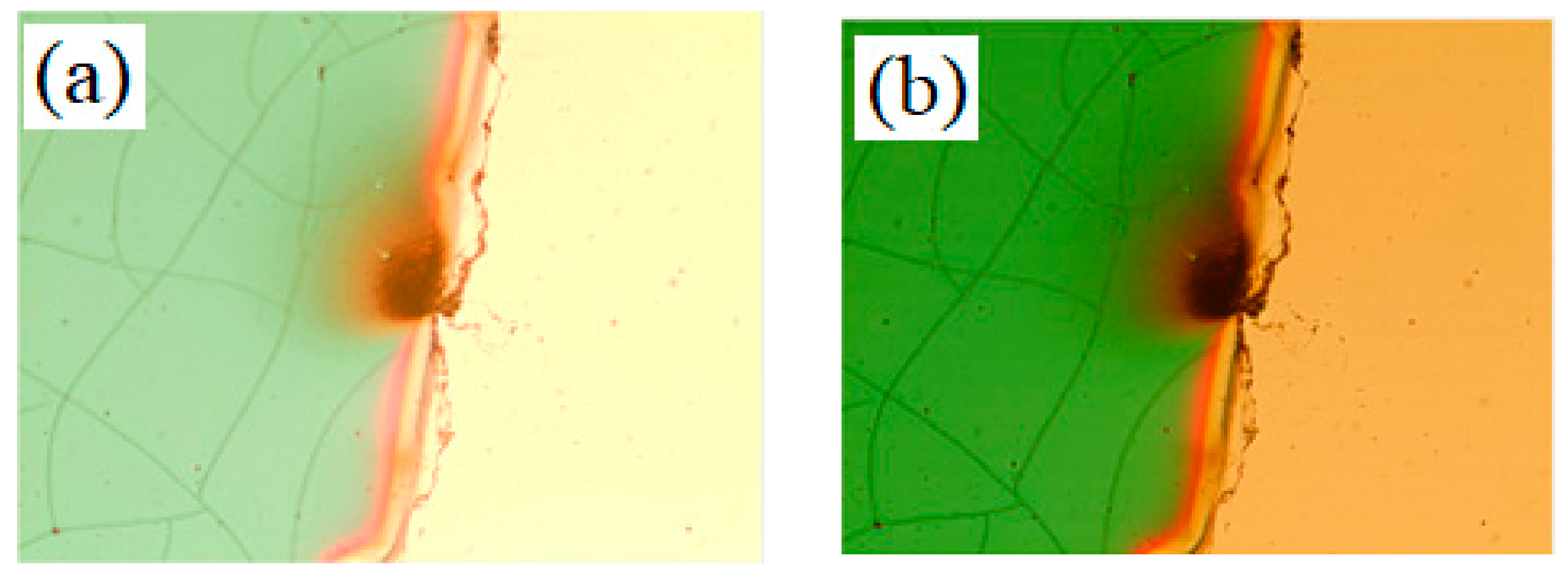
In order to improve visual quality, it is very important to increase contrast. Contrast is the difference in luminance or color that makes an object distinguishable from other objects within the same field of view. In this work, a good image contrast can be obtained by observing the microscopic image using a notch filter. Figure 9 shows a comparison of the microscopic images obtained from the original image and the notch filter with a center wavelength of 480 nm. The left image (original image) has a low contrast because it is difficult to identify the details present in the image as compared to the right image (using 480 nm notch filter). Contrast is defined as (Imax − Imin)/(Imax + Imin); here, Imax and Imin are the highest and lowest intensity value of the image. Using this formula to calculate, the contrast value of the original image is 0.521, and the contrast value of the image using the notch filter is 0.842. Unlike other optical filters, the proposed notch filter can minimize glare and increases the image contrast.
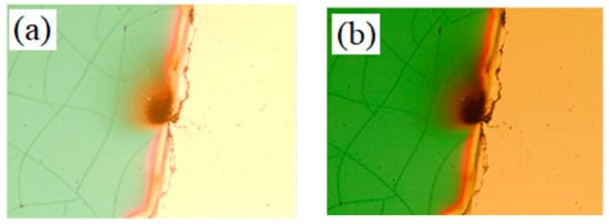
Figure 9.
Microscopic images of (a) original image without filter; (b) using 480 nm notch filter.
4. Conclusions
Notch filters play an important role in analog signal processing as both electronic and optical filters. The synthesis of electronic notch filters possesses a high dynamic range [31]. In this study, a cost-effective notch filter with a center wavelength of 480 nm was prepared by dual electron beam evaporation and ion-assisted deposition technology. The 9-layer notch filter design was simulated by Essential Macleod software. The transmittance of the center wavelength is about 18%, the bandwidth (FWHM) of the notch filter is about 30 nm, and the average transmittance of the transmission band is about 85%. In the wavefront measurement of spectacle lenses, the multi-layer notch filter coating affects the change of the wavefront profile of the spectacle lens. The residual compressive stress of the 9-layer notch filter is 0.235 GPa. Compared with the single-layer film, the compressive stress of the multi-layer film is smaller. The results show that the contribution of residual stress comes not only from the single-layer thin film, but also from the interfacial stress in the multilayer structure. The RMS surface roughness can be reduced from 2.18 nm to 1.85 nm, measured by a self-developed Linnik microscopic interferometer. It also can be seen from the SEM micro-image that the surface morphology of the notch filter is smooth and dense. The SEM micrograph observation is consistent with the measurement results of both residual stress and surface roughness. In addition, a notch filter with a center wavelength of 480 nm is used to observe microscopic images, and a good image contrast can be obtained. These results show that the optical notch filter with a wavelength of 480 nm has low residual stress and low surface roughness.
Author Contributions
Conceptualization and methodology, C.-L.T.; writing—review and editing, C.-L.T.; filter design and measurement, H.-Y.L.; coating experiment and data analysis, K.-S.C.; data curation, C.-Y.C. (Chun-Yu Chiang) and data visualization, C.-Y.C. (Ching-Ying Cheng). All authors have read and agreed to the published version of the manuscript.
Funding
This research was funded by Ministry of Science and Technology of Taiwan for their financial support of this research under Contract number MOST 110-2221-E-035-061. This study was financially supported by Feng Chia University (Contract No. 20H00308) and Chung Shan Medical University.
Institutional Review Board Statement
Not applicable.
Informed Consent Statement
Not applicable.
Data Availability Statement
Not applicable.
Acknowledgments
Authors are grateful for the Precision Instrument Support Center of Feng Chia University in providing SEM analytical facilities.
Conflicts of Interest
The authors declare no conflict of interest.
References
- Leitel, R.; Stenzel, O.; Wilbrandt, S.; Gäbler, D.; Janicki, V.; Kaiser, N. Optical and non-optical characterization of Nb2O5–SiO2 compositional graded-index layers and rugate structures. Thin Solid Film. 2006, 497, 135–141. [Google Scholar] [CrossRef]
- Schallenberg, U.; Ploss, B.; Lappschies, M.; Jakobs, S. Design and manufacturing of high performance notch filters. In Proceedings of the SPIE Conference, San Diego, CA, USA, 27 June–2 July 2010. [Google Scholar]
- Begou, T.; Krol, H.; Stojcevski, D.; Lemarchand, F.; Lequime, M.; Grezes-Besset, C.; Lumeau, J. Complex optical interference filter with stress compensation. In Proceedings of the SPIE Conference, Bellingham, WA, USA, 7–10 September 2015. [Google Scholar]
- Lü, S.; Wang, R.; Ma, J.; Jiang, C.; Mu, J.; Zhao, S.; Yin, X. Design and manufacture of super-multilayer optical filters based on PARMS technology. Adv. Opt. Technol. 2018, 7, 49–55. [Google Scholar] [CrossRef]
- Pervak, V.; Tikhonravov, A.V.; Trubetskov, M.K.; Pistner, J.; Krausz, F.; Apolonski, A. Band filters: Two-material technology versus rugate. Appl. Opt. 2007, 46, 1190–1193. [Google Scholar] [CrossRef]
- Scherer, M.; Schallenberg, U.; Hagedorn, H.; Lehnert, W.; Romanov, B.; Zoeller, A. High performance notch filter coatings produced with PIAD and magnetron sputtering. In Proceedings of the SPIE Conference, Glasgow, Scotland, 2–5 September 2008. [Google Scholar]
- Tien, C.L.; Lin, H.Y.; Cheng, K.S.; Chang, C.K. Design and fabrication of laser protective lenses based on multilayered notch filter with low residual stress and low surface roughness. Coatings 2021, 11, 1513. [Google Scholar] [CrossRef]
- Zhang, J.L.; Tikhonravov, A.V.; Trubetskov, M.K.; Liu, Y.; Cheng, X.; Wang, Z. Design and fabrication of ultra-steep notch filters. Opt. Express 2013, 21, 21523–21529. [Google Scholar] [CrossRef]
- Zhang, J.L.; Xie, Y.J.; Cheng, X.B.; Jiao, H.F.; Wang, Z.S. Thin-film thickness-modulated designs for optical minus filter. Appl. Opt. 2013, 52, 5788–5793. [Google Scholar] [CrossRef]
- Noell, W.K.; Walker, V.S.; Kang, B.S.; Berman, S. Retinal damage by light in rats. Investig. Ophthalmol. 1966, 5, 450–473. [Google Scholar]
- Ham, W.T., Jr.; Ruffolo, J.J., Jr.; Mueller, H.A., Jr.; Guerry, D. The nature of retinal radiation damage: Dependence on wavelength, power level and exposure time. Vis. Res. 1980, 20, 1105–1111. [Google Scholar] [CrossRef]
- Ham, W.T., Jr.; Ruffolo, J.J., Jr.; Mueller, H.A.; Clarke, A.M.; Moon, M.E. Histologic analysis of photochemical lesions produced in rhesus retina by short-wave-length light. Investig. Ophthalmol. Vis. Sci. 1978, 17, 1029–1035. [Google Scholar]
- Ham, W.T., Jr.; Mueller, H.A.; Ruffolo, J.J., Jr.; Clarke, A.M. Sensitivity of the retina to radiation damage as a function of wavelength. Photochem. Photobiol. 1979, 29, 735–743. [Google Scholar] [CrossRef]
- Ham, W.T., Jr.; Mueller, H.A.; Sliney, D.H. Retinal sensitivity to damage from short wavelength light. Nature 1976, 260, 153–155. [Google Scholar] [CrossRef] [PubMed]
- Kiser, A.K.; Deschler, E.K.; Dagnelie, G. Visual function and performance with blue-light blocking filters in age-related macular degeneration. Clin. Exp. Ophthalmol. 2008, 36, 514–520. [Google Scholar] [CrossRef] [PubMed]
- Allan, S.T.; Herrington, B.; Cole, C.; Mackrodt, K.; Slim, T.; Lingwood, D. Rugate coating for an avionics head-up-display. In Proceedings of the SPIE Conference, Orlando, FL, USA, 14–16 April 2004; pp. 130–137. [Google Scholar]
- Shankar, A.; Kumar, S. Using a pair of antireflection layer in a minus filter to suppress ripples in the HUD-beam combiner. J. Opt. 2014, 43, 257–259. [Google Scholar] [CrossRef]
- Lyngnes, O.; Kraus, J. Design of optical notch filters using apodized thickness modulation. Appl. Opt. 2014, 53, A21–A26. [Google Scholar] [CrossRef]
- Hoggan, R.N.; Subhash, A.; Blair, S.; Digre, K.B.; Baggaley, S.K.; Gordon, J.; Brennan, K.C.; Warner, J.E.A.; Crum, A.V.; Katz, B.J. Thin-film optical notch filter spectacle coatis for the treatment of migraine and photophobia. J. Clin. Neurosci. 2016, 28, 71–76. [Google Scholar] [CrossRef] [PubMed] [Green Version]
- Kumar, M.; Kumari, N.; Sharma, A.L.; Karar, V.; Sinha, R.K. Design and fabrication of reflective notch filter using modified thickness modulated Al2O3-SiO2 multilayer. In Proceedings of the OSA Technical Digest in Optical Interference Coatings Conference, Santa Ana Pueblo, New Mexico, 2–7 June 2019. [Google Scholar]
- Kumar, V.S.R.S.P.; Kumar, M.; Kumari, N.; Sharma, A.L. Design and development of an optical reflective notch filter using the ion assisted deposition technique with stepwise modulated thickness for avionics applications. Appl. Opt. 2020, 59, 564–571. [Google Scholar] [CrossRef] [PubMed]
- MacLeod, H.A. Thin-Film Optical Filters, 4th ed.; CRC Press: Boca Raton, FL, USA, 2010. [Google Scholar]
- Tien, C.L.; Zeng, H.D. Measuring residual stress of anisotropic thin film by fast Fourier transform. Opt. Express 2010, 18, 16594–16600. [Google Scholar] [CrossRef]
- Takeda, M.; Ina, H.; Kobayashi, S. Fourier-transform method of fringe-pattern analysis for computer-based topography and interferometr. Appl. Opt. 1982, 72, 156–160. [Google Scholar]
- Macy, W.W., Jr. Two-dimensional fringe-pattern analysis. Appl. Opt. 1983, 22, 3898–3901. [Google Scholar] [CrossRef]
- Stoney, G.G. The tension of metallic films deposited by electrolysis. Proc. R. Soc. Lond. 1909, 86, 172–175. [Google Scholar]
- Tien, C.L.; Yang, H.M.; Liu, M.C. The measurement of surface roughness of optical thin films based on fast Fourier transform. Thin Solid Film. 2009, 517, 5110–5115. [Google Scholar] [CrossRef]
- Tien, C.L.; Yu, K.C.; Tsai, T.Y.; Lin, C.S.; Li, C.Y. Measurement of surface roughness of thin films by a hybrid interference microscope with different phase algorithms. Appl. Opt. 2014, 53, H213–H219. [Google Scholar] [CrossRef] [PubMed]
- Goldstein, J.I.; Newbury, D.E.; Echlin, P.; Joy, D.C.; Fiori, C.; Lifshin, E. Scanning Electron Microscopy and X-ray Microanalysis; Plenum Press: New York, NY, USA, 1981. [Google Scholar]
- Elsholz, F.; Schöll, E.; Rosenfeld, A. Control of surface roughness in amorphous thin-film growth. Appl. Phys. Lett. 2004, 84, 4167–4169. [Google Scholar] [CrossRef]
- Metin, B.; Minaei, S.; Cicekoglu, O. Enhanced dynamic range analog filter topologies with a notch/all-pass circuit example. Analog. Integr. Circuits Signal Processing 2007, 51, 181–189. [Google Scholar] [CrossRef]


Publisher’s Note: MDPI stays neutral with regard to jurisdictional claims in published maps and institutional affiliations. |
© 2021 by the authors. Licensee MDPI, Basel, Switzerland. This article is an open access article distributed under the terms and conditions of the Creative Commons Attribution (CC BY) license (https://creativecommons.org/licenses/by/4.0/).