1. Introduction
Reflections and fog are major problems that affect the efficiency of light collection and image peculiarity of optical components. Reflections not only induce glare and ghost images, but also diminish the availability of incident light. Fog can increase reflectivity and unpreventably cut down the clarity of transparent surfaces, leading to cumbersome and imaginably perilous hindrances in everyday life. Especially in cold and humid environments, fog can freeze and turn to frost, which completely prevents light from passing through a surface. Therefore, it is strikingly fascinating to achieve a highly transparent surface that incorporates both antireflective and antifogging properties.
In order to broaden its scope of application, recent developments in the field of antireflection have led to a renewed interest in multifunctional antireflective surfaces [
1,
2,
3,
4,
5,
6,
7,
8]. A considerable amount of literature has been concentrated on constructing multifunctional polymer coatings with antireflection and antifogging behaviors. Particularly in silicon solar cell technology [
9,
10,
11,
12], texturing of oriented monocrystalline silicon ⟨100⟩ substrates, and subsequently an antireflective coating, which was deposited, has turned into an acknowledged approach for a greater probability to reduce reflection loss. When compared with the random pyramid structure, which is widely distributed in size and shape, the inverted pyramid structure has a more efficient light-capturing geometry [
13,
14]. The total surface area of this structure is only 1.7 times that of the flat surface, which minimizes the surface compound loss.
However, these prepared coatings may readily exfoliate from the substrate by virtue of the poor mechanical characteristics and differential thermal expansion. Accordingly, besides attractive antireflective performance, one of the most significant current discussions concerning antireflective coatings is that they should display favorable mechanical properties: durability, adhesion, and wear resistance [
15,
16,
17]. It is well known that optical polymer has remarkable advantages in chemical stability, such as low cost, easy and fast processing, etc. Among these advantages, the plexiglass (polymethylmethacrylate), is also known as an acrylic that has magnificent light transmission performance, which can transmit more than 92% of sunlight, tolerance to heat and cold, corrosion resistance, easily soluble in organic solvents and so forth. Thus, it can be used in the transparent structural components, such as lenses, sports eyewear, transparent displays, and sensors [
18].
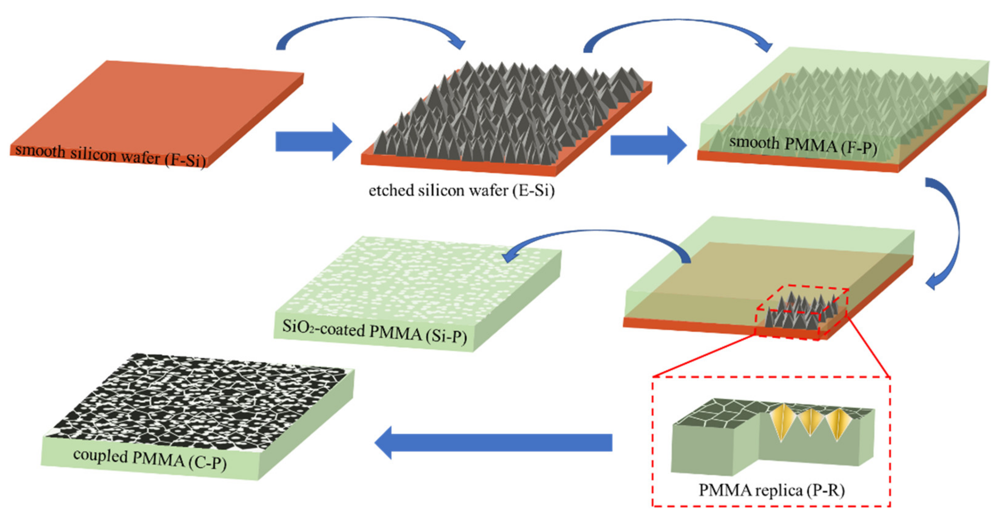
In this work, a thin film with excellent antireflective and antifogging (AF) properties was designed and fabricated on polymethylmethacrylate (PMMA) substrate. The structure and composition of the film were characterized by using scanning electron microscopy (SEM) and Fourier Transform Infrared Spectroscopy (FTIR), the optical properties and AF properties of the film were evaluated using spectroscopy and steam tests, respectively. The mechanical properties of the film were tested by means of Shore hardness, sandpaper friction and tape peeling. The test results show that the combination of inverted pyramid microstructure array and hydrophilic SiO2 nanoparticles not only effectively reduces the refractive index of the film, but also improves the surface energy of the film to a large extent, thus giving the film excellent superhydrophilic, antireflective and AF properties. Moreover, the addition of the silane coupling agent (KH550) significantly improved the binding between nanoparticles and PMMA substrate, resulting in superior mechanical properties of the film.
2. Experimental Section
2.1. Materials and Chemical Reagents
The single-crystal silicon wafers (commercially available single-side polished, crystal direction ⟨100⟩) were purchased from the Research Material Micro-Nano Technology Co., Ltd (Suzhou, China). The deionized water, acetone, anhydrous ethanol, isopropyl alcohol, sodium hydroxide, hydrogen peroxide, hydrochloric acid, hydrofluoric acid and ammonia water were purchased from commercial sources in the highest available purity. The tetraethoxysilane was obtained from the Xinya Chemical Co., Ltd (Zhang Jiagang, China). The PMMA powder was purchased from Dinghai Plastic & Chemical Co., Ltd (Dongguan, China). Toluene was purchased from Aladdin. The silane coupling agent (KH550) was purchased from Shanyi Plastic Co., Ltd (Dongguan, China).
2.2. Silicon Wafer Cleaning
The 0.1 Ωcm resistivity, 0.5 mm thickness, wafer ⟨100⟩ single-crystal Si was selected for these experiments. The specific steps in the wafer cleaning process are as follows: (1) first, wafer (1 cm × 2 cm) was ultrasonically shaken in acetone for 10 min to remove the organics on the substrate surface; then in anhydrous ethanol for 10 min to remove residual acetone; and finally in deionized water for 10 min to remove the substrate’s inorganics; (2) the silicon wafer was put into a mixture solution of NH3.H2O, H2O2 and deionized water (volume ratio 1:1.5:5) and boiled, then the wafer was placed in a solution of HCl, H2O2 and deionized water (volume ratio 1:1:5) boiled for 5 min, and subsequently rinsed with deionized water. The above steps were taken to remove metallic impurities from the silicon; (3) the silicon wafer was put into a solution of HF and deionized water (volume ratio of 1:20) and soaked for 6 s, with the purpose of removing the oxide layer on the surface, then sonicated with deionized water for 15 min and dried.
2.3. Preparation of Pyramid Microstructures
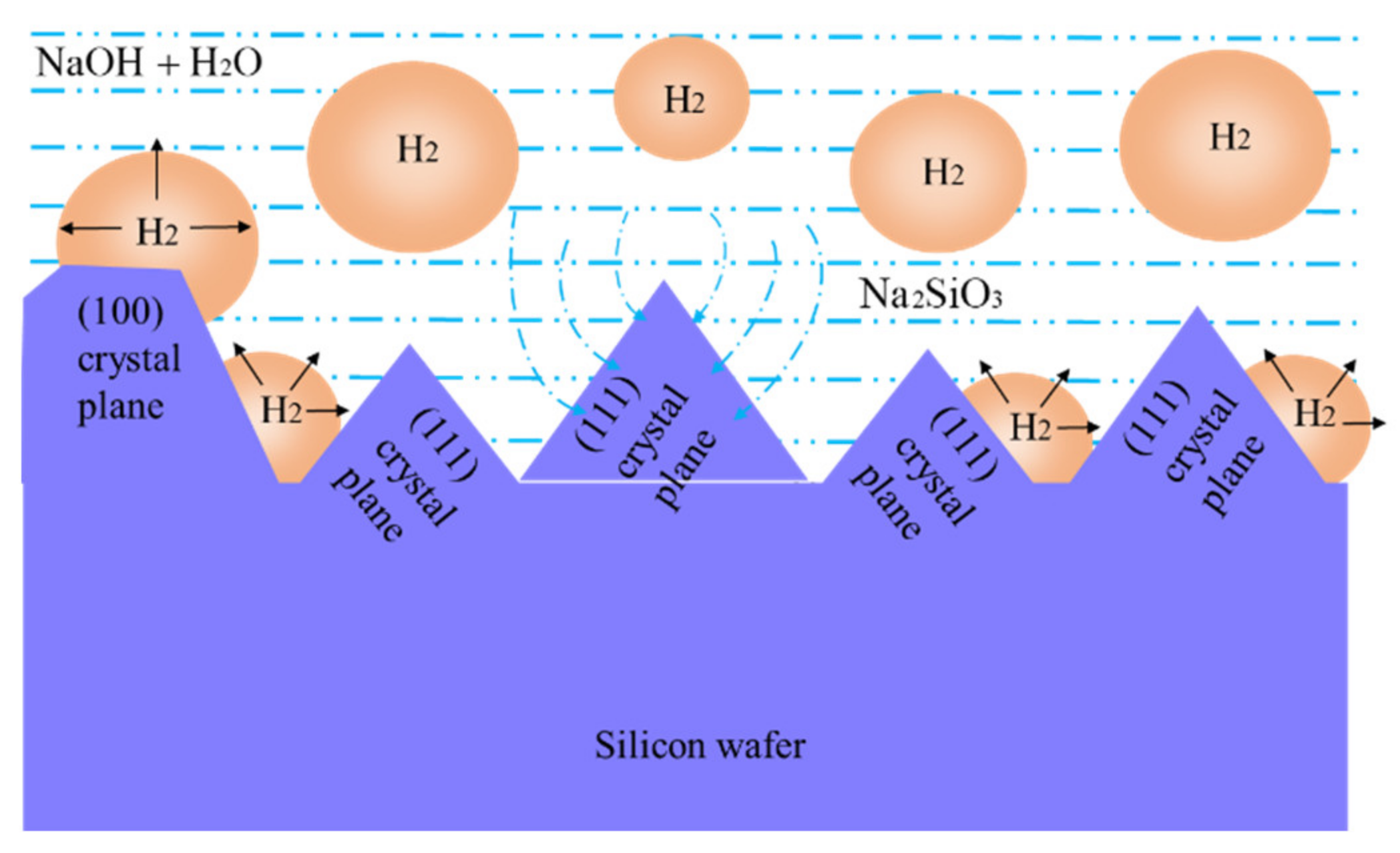
A NaOH solution of 12% by mass fraction was configured, and a solution of isopropyl alcohol (IPA) of 10% by volume was added to the solution. The clean silicon wafer was immersed in the configured solution, and heated in a constant temperature water bath at 82 °C for 35 min. After etching the wafer, the wafer was rinsed with deionized water, then put it into 10% HCl solution for 1 min and 10% HF solution for 10 s, respectively, to remove the metal impurities and oxide layer on the wafer surface. Finally, the wafer was ultrasonically cleaned in deionized water for 1 min, to remove the residual surface liquid. Using the anisotropic corrosion of silicon in a low-concentration alkaline solution, the corrosion rate of silicon on the (111) crystal face is lower than that of other crystal planes, especially the (100) crystal face. The corrosion rate of the (100) crystal plane, which is about 10–35 times higher than that of the (111) crystal face, due to the strong dependence of the etching rate on the crystal orientation, after a certain period of corrosion, leaves a four-sided pyramid consisting of the (111) face on the surface of the (100) single-crystal silicon wafer [
19]. However, due to the generation of H
2 during the etching process, these bubbles will adhere to the wafer surface, resulting in the formation of pyramids with random distribution and uneven sizes (
Figure 1).
2.4. Preparation of Inverted Pyramid Microstructures
The PMMA and toluene were mixed at a mass ratio of 1:14 and stirred at 70 °C for 30 min. Immediately afterwards, the precursor solution was spin-coated onto the etched silicon wafer, and the whole sample was cured at 45 °C for 6 h, followed by curing at 80 °C for 4 h to completely evaporate the solvent. Finally, the PMMA sample was gently peeled off from the silicon wafer.
2.5. Preparation of Coupled PMMA Film
Tetraethoxysilane (TEOS), ethanol, deionized water and ammonia were mixed in a volume ratio of 1:2.5:4:0.5, the solution was continuously stirred on a magnetic stirrer at 50 °C for 2 h, which was then aged in an oven at 30 °C for 72 h. Finally, the obtained solution was refluxed at 80 °C for 24 h to remove the ammonia. The silica sol was dispersed in xylene with ultrasonic vibration for 1 h, then a certain amount of coupling agent (KH550) was added. The mixed solution was stirred continuously at 80 °C for 2 h, and then cooled to room temperature. The KH550-grafted nanoparticles in the above suspension were separated by high-speed centrifugation, washed with ethanol several times, dried in vacuum at room temperature for 6 h, and finally sprayed onto the PMMA sample, then heated in an oven at 100 °C for 1 h.
2.6. Characteristics
The surface morphology of the fabricated sample was observed by means of FESEM (JSM-6700LF, JEOL, Tokyo, Japan) at an accelerating voltage of 20 kV, a working distance of 14.1 mm and observation mode (low magnification, SE2), and the nano-SiO2 particles were characterized by AFM (Bruker Dimension Icon, Tempe, AZ, USA). The static water contact angles of the sample surfaces were estimated with an optical contact angle measuring device (OCA20 data physics, Filderstadt, Germany), a droplet (3 µL) was dropped on four different surfaces in turn based on a sessile drop technique, and each sample was measured five times at room temperature. The chemical bonds of the samples were examined using Fourier Transform Infrared Spectroscopy (IRAffinity-1S, FTIR, Shimadzu, Japan). The reflectance and transmittance spectra of each sample were obtained using a miniature fiber-optic spectrometer (Ocean Optics, Tallahassee, FL, USA) at normal incidence over a wavelength range of 400−800 nm, and the light spot size of the incident beam was about 5 mm in diameter. The spectrometer was carefully calibrated with STD-WS, a standard white board certified by the National Institute of Metrology of China. Hardness measurements were performed by a Shore digital hardness tester (Zwick R5LB041, Ulm, Germany) according to GB/T 2411 standard. Recorded hardness values represented an average value of at least five samples with standard deviations.
3. Results and Discussion
3.1. SEM Characterization of the Inverted Pyramid Microstructures
The schematic drawing of the sample preparation procedure is shown in
Figure 2.
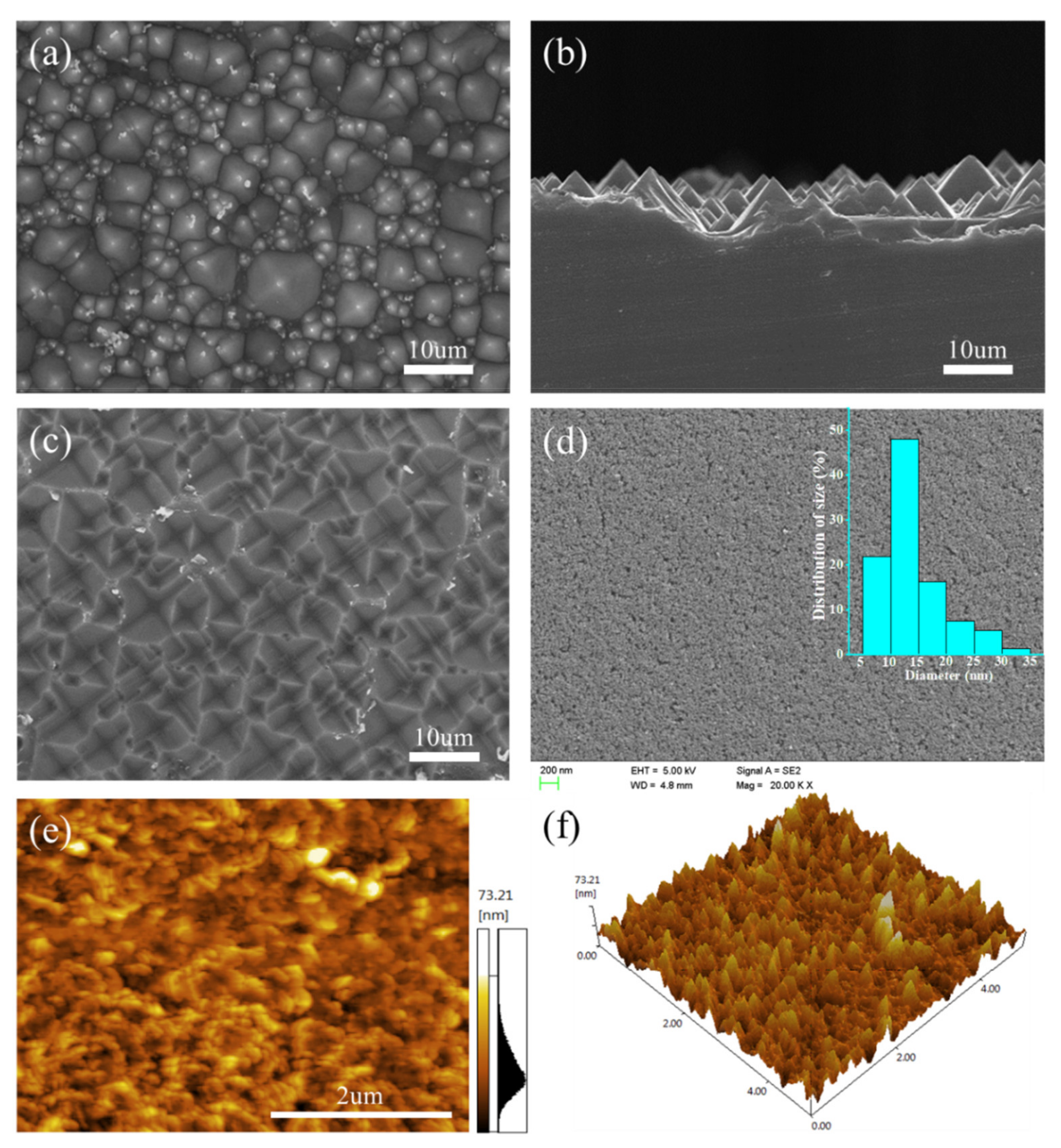
Figure 3a,b shows the SEM images of the etched silicon wafer. It can be seen that the orientation position and size distribution of each pyramid microstructure is random. The bottom side of the pyramid is 1–7 μm in length, the height is 1–5 μm. The top angle is 70–75°, and almost every pyramid partially overlaps with several adjacent pyramids of different sizes; the surface of the triangular pyramid is smooth.
Figure 3c shows the surface morphology of the PMMA replica. It can be seen that the micro-transfer printing method is quite successful; inverted pyramids of different sizes are staggered on the PMMA substrate surface.
Figure 3d shows the surface morphology of the nanoparticles. It is obvious that the surface of the coating is nanoporous. It was found from the particle size and its distribution that nearly 50% of the particles were in the range of 10–15 nm, about 21% of the particles size were in the range of 5–10 nm, about 16% of the particles size were in the range of 15–20 nm; just 13% of the particles were above 20 nm. Worth noting as well are the uniformly distributed nanopores on the surface, which enhance the wettability of the surface, making it more superhydrophilic.
3.2. Optical Properties of Coupled PMMA Film
3.2.1. Comparative Analysis of Reflectance Spectra
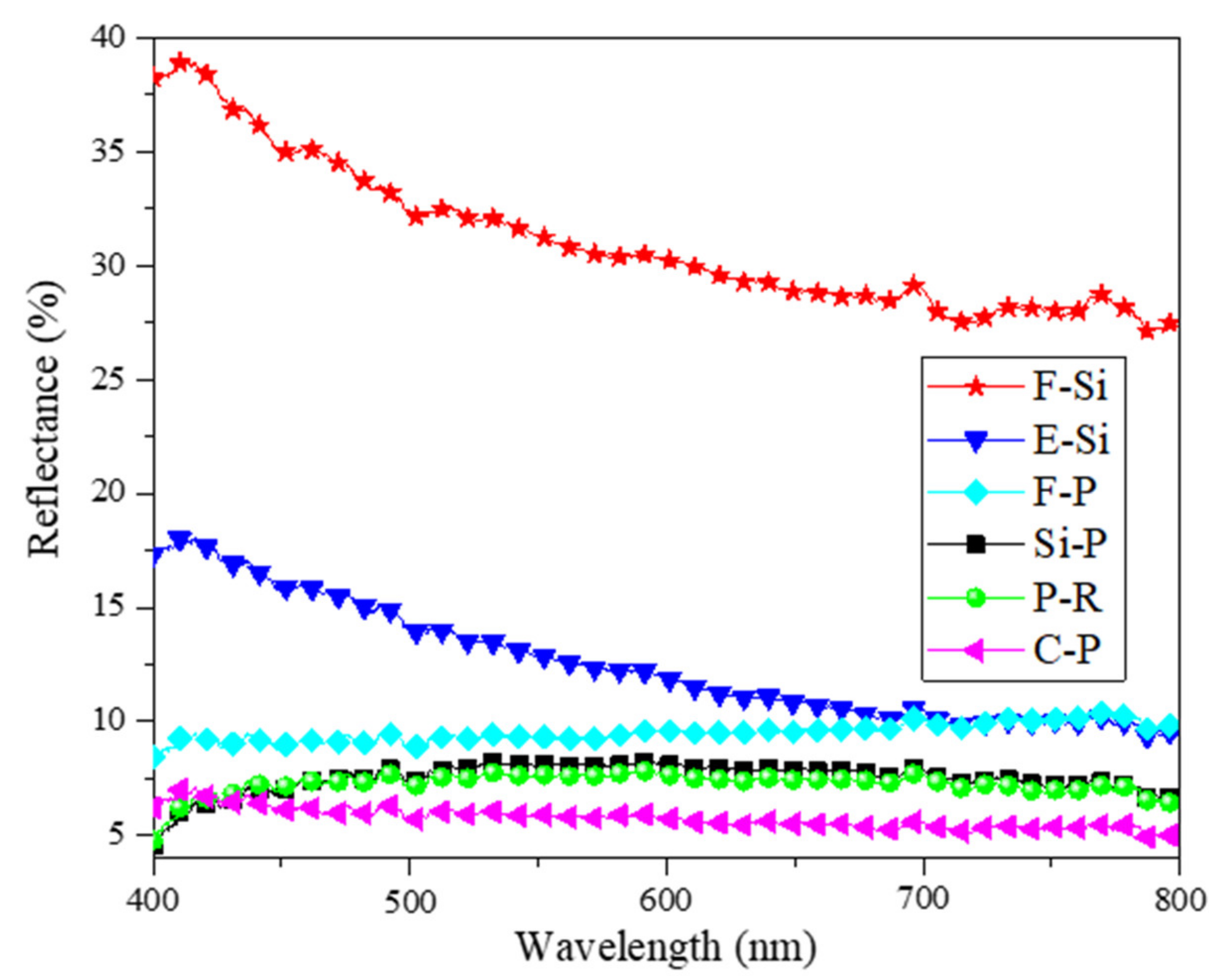
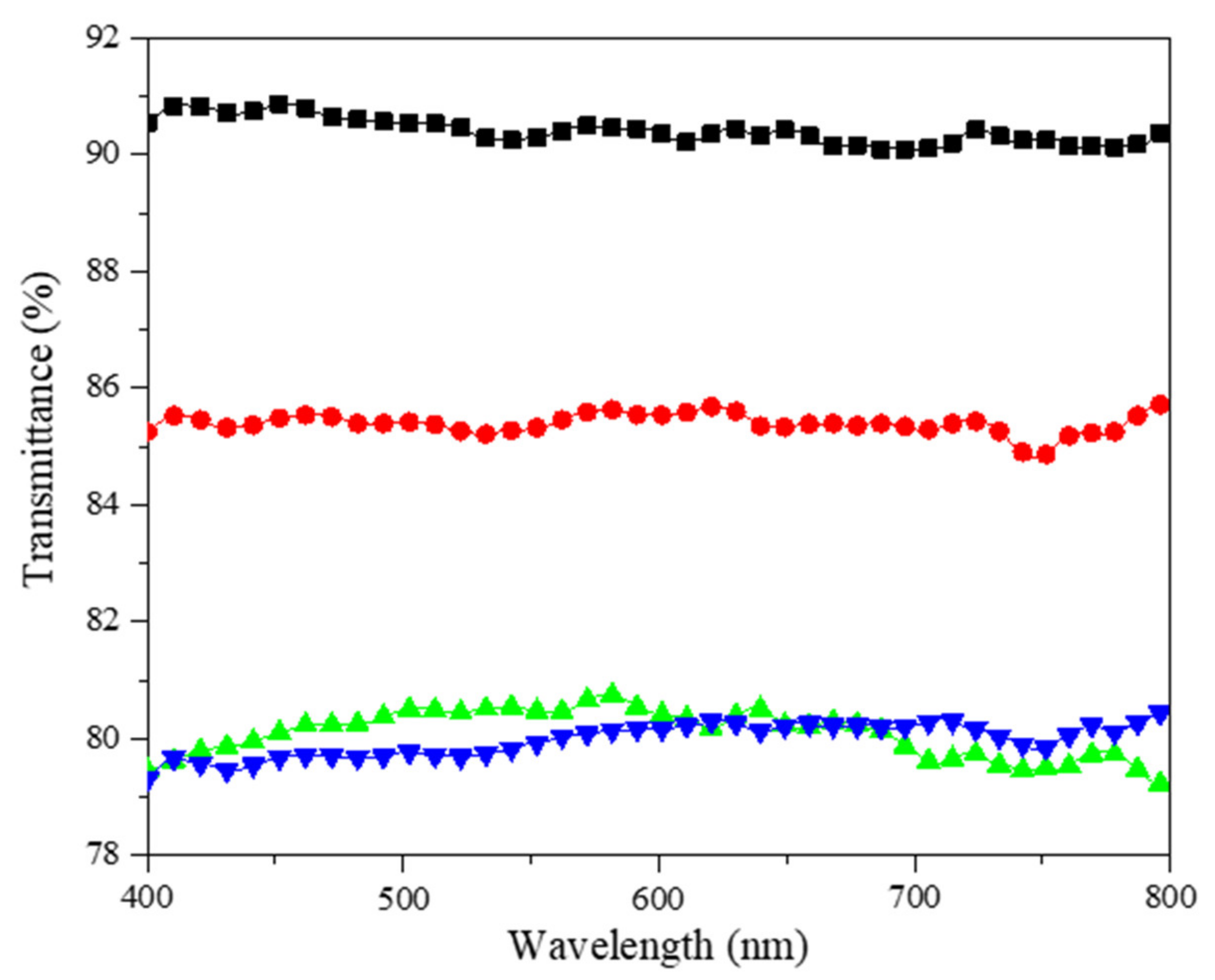
Figure 4 shows the reflectance spectra of smooth silicon wafer (F-Si), etched silicon wafer (E-Si), smooth PMMA (F-P), SiO
2-coated PMMA (Si-P), PMMA replica (P-R), and coupled PMMA (C-P), respectively. In the visible wavelength range (400–800 nm), the average reflectance of E-Si and C-P is much lower than that of F-Si and F-P, and this trapped light effect is mainly attributed to the surface microstructure.
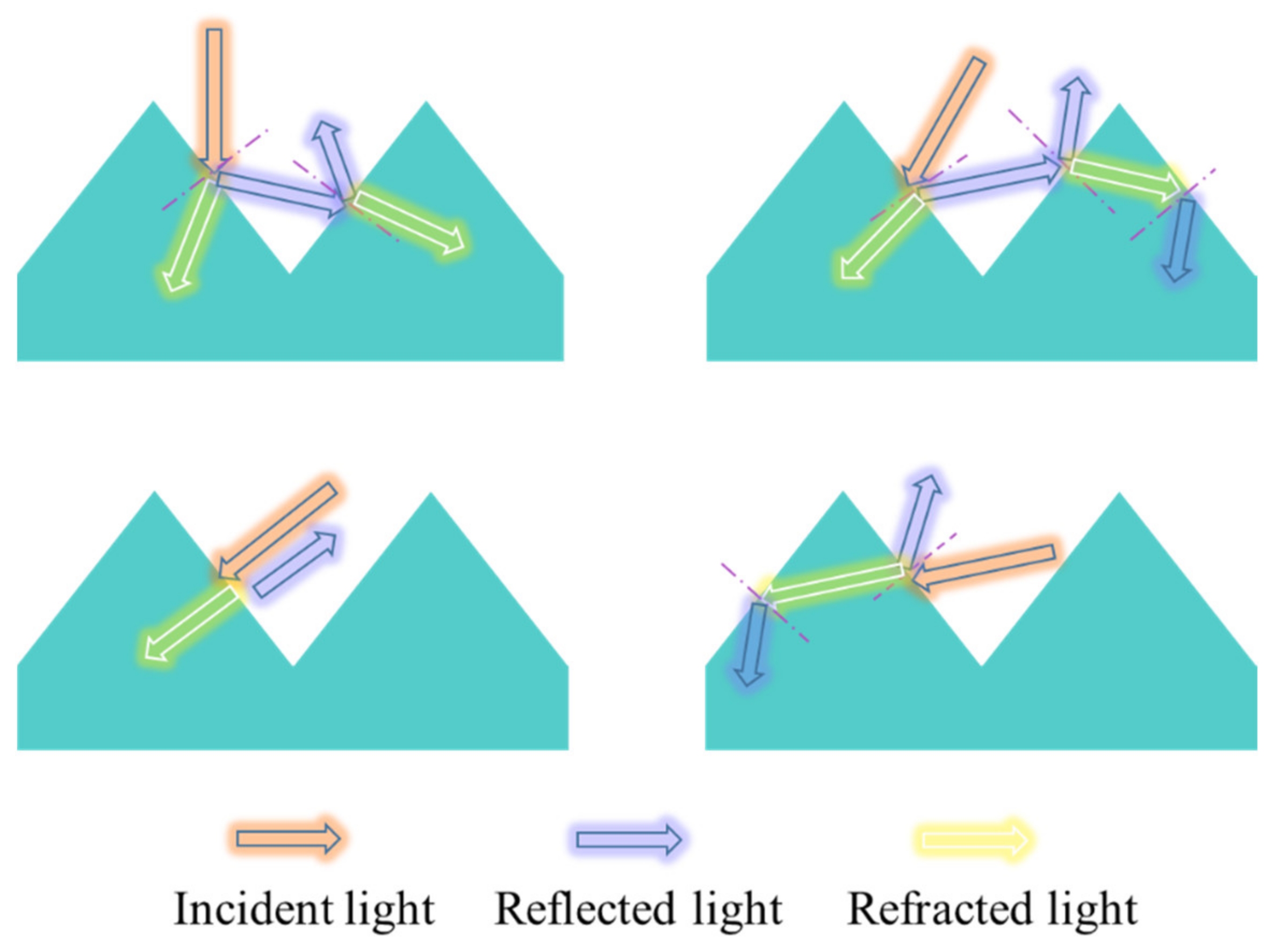
Figure 4 is a schematic diagram of the light trapping effect of the inverted pyramid microstructure. For incident light at different angles, most of the light can be transmitted from the air into the C-P sample after the first passage, and only a small amount of light will be reflected onto the adjacent pyramid surface. Most of the reflected light then enters and is reflected inside the C-P sample after the second pass.
3.2.2. Comparative Analysis of Transmission Spectra
Ideally, the trapped light structure can not only reduce the reflection loss of the surface, but also increase the surface transmittance. The schematic diagram of the light trapping effect of pyramids was shown in
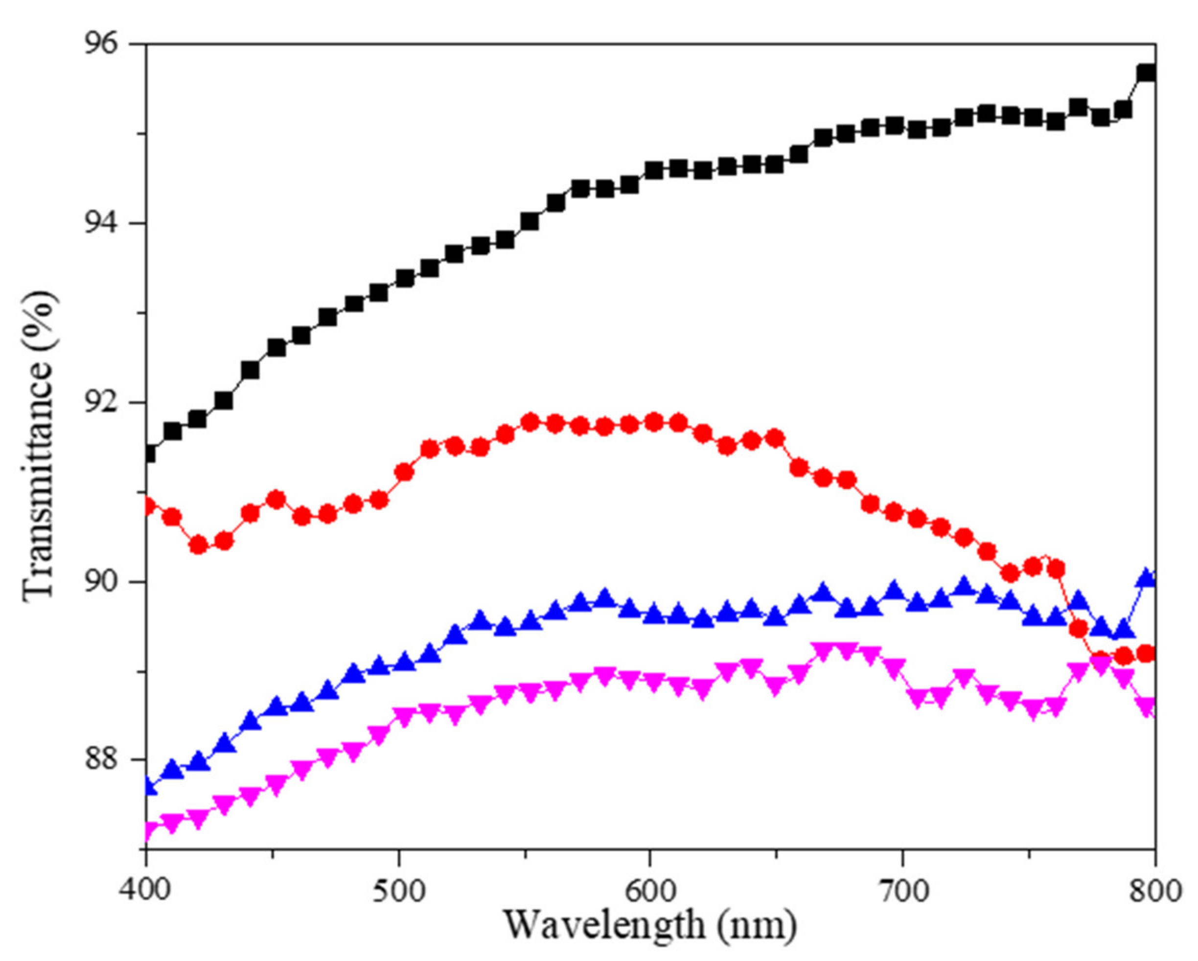
Figure 5. For incident light at different angles, most of the light transmits from air into the PMMA replica after its first pass; only a small amount is reflected onto a neighboring pyramid. Furthermore, a large fraction of the reflected light enters and is reflected inside the concave surface of the inverted pyramid after the second pass. Therefore, quasi-omnidirectionality (i.e., less angle-dependency of the reflectance—transmittance characteristic) can be achieved in inverted pyramid structured surfaces. On the other hand, the random distribution of pyramids plays a crucial role in light trapping effects. Compared to the surface with uniform pyramids, the surface with staggered and differently sized pyramids displays a much lower reflectance and improved transmittance. Moreover, the concave of the inverted pyramid facilitates the inhibition of reflection losses. Hence, the light trapping effect of the molded PMMA replica originates from the randomly distributed pyramids with their different sizes and concaves. As shown in
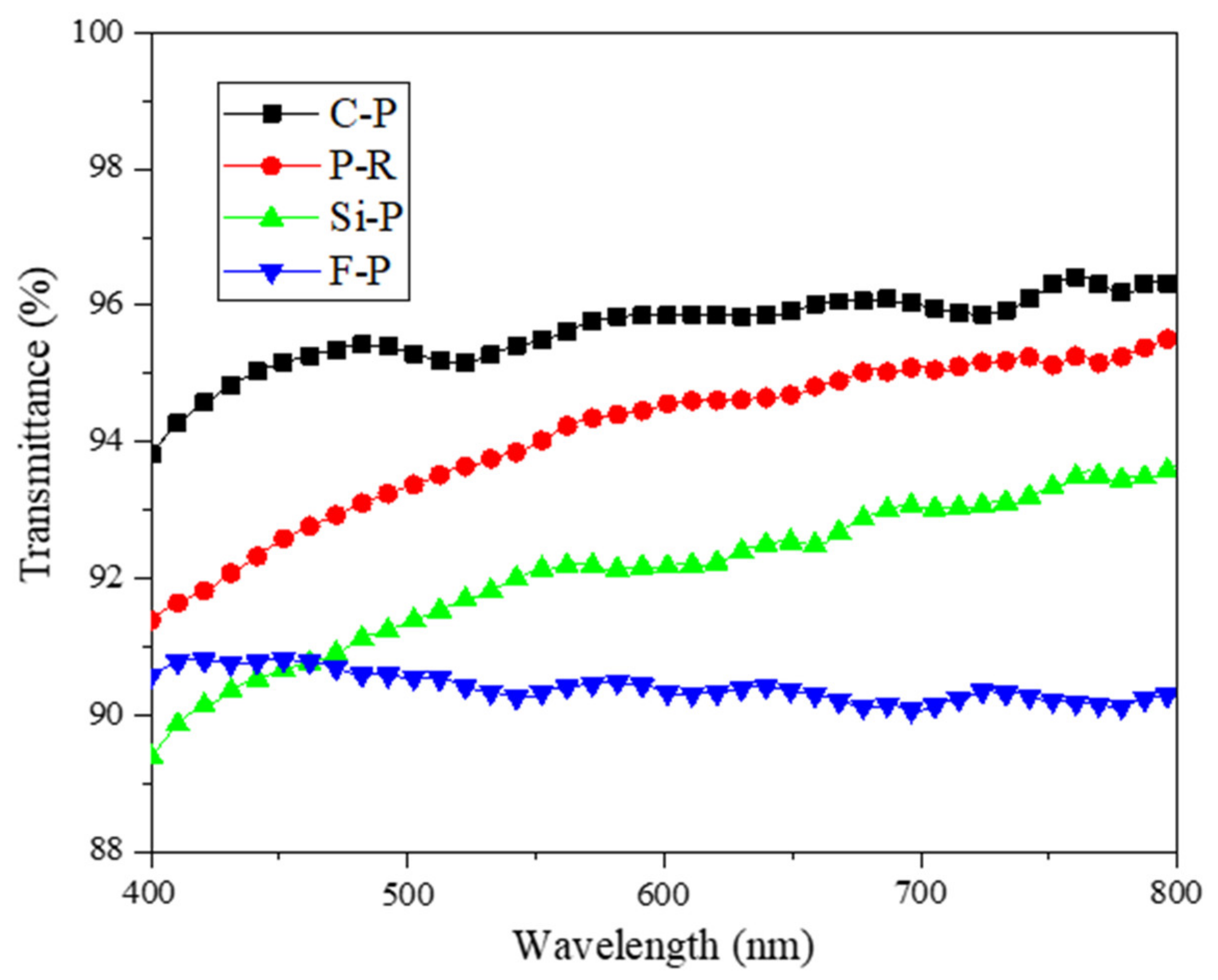
Figure 6, in the wavelength range of 400–800 nm, the average transmittance of the P-R sample is 92.85%, and the maximum transmittance of the P-R film is as high as 95%, while the average transmittance of the F-P sample is 90.62%, and the maximum transmittance is less than 91%. Next, the reasons for the decline of reflectance and increment in transmittance of the P-R sample were analyzed. The increase in roughness of the PMMA surface causes multiple reflections of the incident light inside the inverted pyramid, leading to an increase in the travel path of the incident light and thereby increasing the light absorption rate [
20]. Consequently, on the surface of the inverted pyramid microstructure, the incident light can be strongly coupled into the P-R film, which significantly weakens the dependence of the antireflection effect on the incident angle [
21].
In general, the increase in the surface roughness of the film is conducive to the improvement of superhydrophilicity, but is usually detrimental to the improvement of transparency, because the light scattering on the rough surface is more severe. Therefore, the surface roughness should be regulated below 100 nm to reduce light scattering and obtain a highly transparent film. When silica sol is sprayed onto the P-R sample, a superhydrophilic nano-SiO
2 film will be formed on the top. On the one hand, air will enter the nanoparticle layer, which declines the refractive index of the top layer, and a lower refractive index contributes to augmenting transmission of the film [
22,
23]. On the other hand, the optical properties of the film are affected by the interlayer particle structure [
24]; the granular structure of the top layer not only causes the incident light to be scattered at different angles, but also concentrates the incident light. The incident light preferentially penetrates the film, which improves the light transmittance of the C-P film. The AFM result (
Figure 3e,f also indicates that the increase in surface roughness did not unfavorably affect the transmittance because it was below 70 nm. Thus, it can be seen in
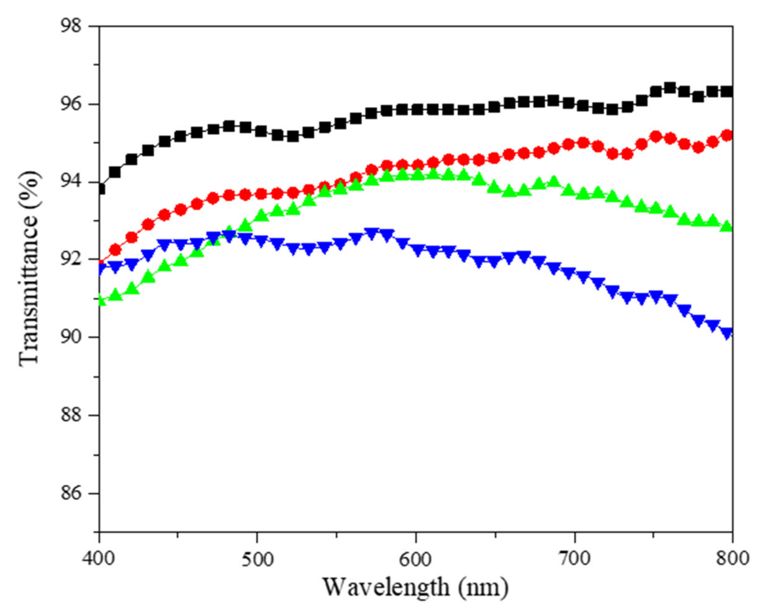
Figure 6 that the average transmittance (95.87%) of the C-P sample at visible wavelengths of 400–800 nm is higher than that of the Si-P sample (92.36%) and the P-R sample (92.85%), with the maximum transmittance of the C-P sample is beyond 96%. In the wavelength range of 400–800 nm, the average transmittance increased from 90.62% of F-P to 95.87% for C-P film, and the maximum transmittance at 765 nm was 96.21%.
3.3. Antifogging Properties of Coupled PMMA Film
3.3.1. Comparative Analysis of Transmittance Rate before and after Spraying
In order to quantify the AF performance of C-P film, we measured the light transmittance of F-P, P-R, and C-P film before and after spraying. The mist generated by an ultrasonic humidifier was sprayed on the surface of the sample in sequence. The ambient temperature of the test room is 25 °C, the humidity is 75%, and the spraying time is gradually increased at a time interval of 2 min. The change in transmittance of the sample surface in the wavelength range of 400 to 800 nm was observed. After each transmission spectrum was collected, the sample surface was blown dry, and it finally formed a dynamic cycle of “spray-blow-dry-spray”.
As shown in
Figure 7, the F-P film was sequentially sprayed by the generated fog for 6 min; the average transmittance significantly decreased to 78.35%, while the average transmittance slightly reduced to 88.78% after spraying for 6 min for the P-R film (
Figure 8). It was obvious that the presence of this inverted pyramid structure greatly increases the transparency of the PMMA. Interestingly, although the transmittance of C-P film was also affected after spraying, the average transmittance of C-P film with respect to the same spray times remained around 92.26% over a range of wavelengths from 400 to 800 nm (
Figure 9). It was confirmed that the C-P film demonstrates high antifogging performance over visible wavelengths.
3.3.2. Steam Test
In order to more closely examine the AF performance of the C-P film, the AF effect on the sample surface was observed using a steam test (100 °C water vapor for 10 s). The C-P and F-P films were respectively clamped with dovetail clamps, and simultaneously placed directly above the beaker containing half a cup of boiling water, with the sample surface facing downward. In the course of the test, it was found that water vapor quickly condensed on the surface of the F-P sample, making the F-P film blurred, and it was difficult to see the letters under the beaker, as shown in
Figure 10a. In comparison, after 10 s, although the inner wall of the beaker was covered with water vapor, the C-P film remained transparent, and the letters below the beaker were clearly visible (
Figure 10b). The above results fully indicate that the C-P film has the more favorable AF performance.
3.4. Mechanical Properties of Coupled PMMA Film
In order to facilitate practical applications, it was, therefore, necessary to test the mechanical properties of the C-P film, including hardness, abrasion resistance and adhesion. In order to ensure the bonding between the superhydrophilic nano-SiO2 particles and the P-R substrate, the silane coupling agent KH550 was used as the cross-linked structure of the C-P film. The hardness of the film was mensurated by the GB/T 2411 “Plastic Shore Hardness Test Method”, the wear resistance of the surface coating was determined by the sandpaper friction test, and the adhesion of the film surface coating was evaluated by the tape peel test.
3.4.1. Hardness Test
According to GB/T 2411 “Plastic Shore Hardness Test Method” [
25], the hardness measurement results of P-R and C-P films are shown in
Table 1. The test results show that the hardness of the C-P film increased by 2.8 (HD) when compared with the P-R film.
3.4.2. Abrasion Resistance Test
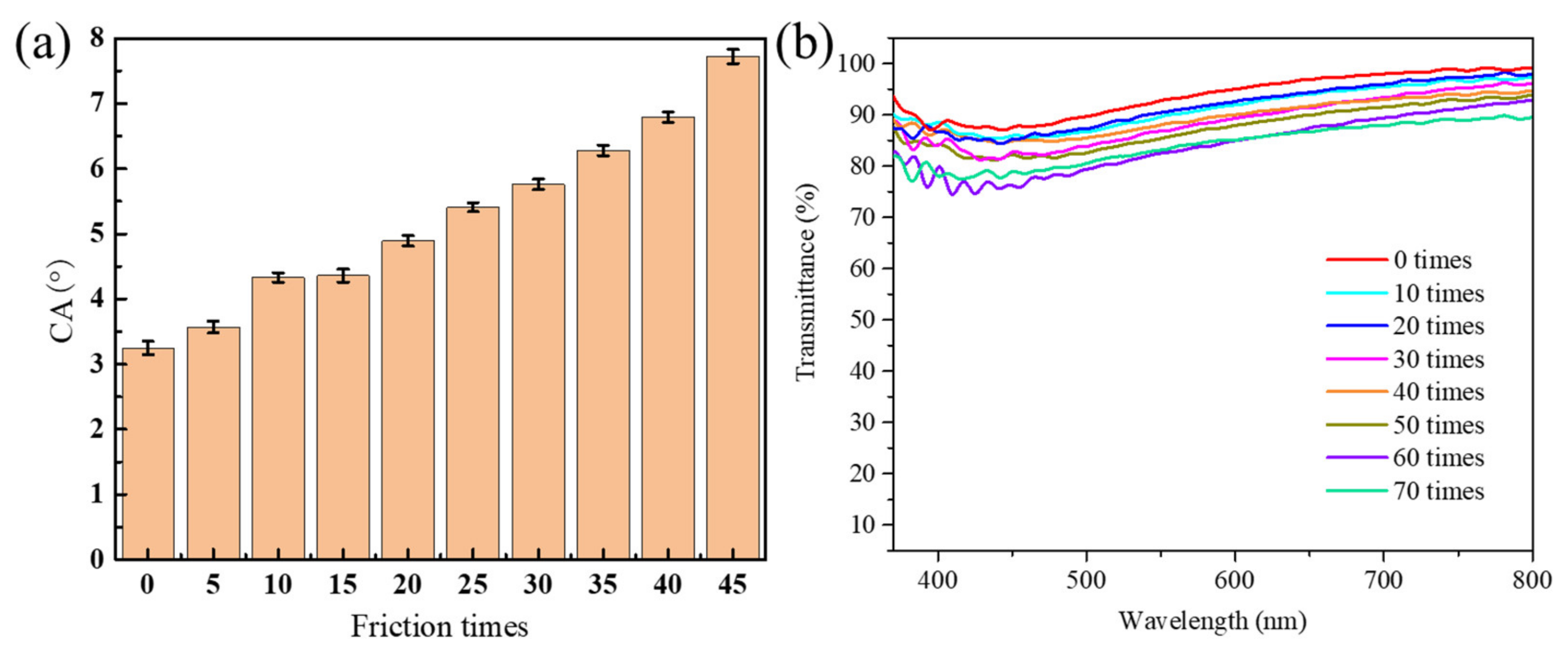
In addition, when 800# SiC sandpaper was used as the wear material and 40 g weight as the load, the C-P film moved back and forth at a speed of 2 cm/s. The variation of the contact angle is influenced by the amount of friction, as shown in
Figure 11a, which shows that the surface contact angle (CA) gradually rises with the increment of the friction numbers, and when the numbers of friction reach to 25 times, the average CA of the film augmented lightly from 3.17° to 4.76°; when the friction frequency was increased to 45 times, the CA of the film turned to 7.72°, still maintaining its superhydrophilic properties. Subsequently, the transmittance of C-P film after the friction test is shown in
Figure 11b; the trend of these curves was roughly the same for most of the wavelengths considered. It can be seen that the average transmittance of the coupled film is maintained at 93.78% after friction 10 times, and after friction 50 times, it is close to 90%; however, after friction 60 times, the average transmittance is only 84.2%, and the optical characteristics are basically consistent with the results of the wettability. Thus, the friction test results indicate that the prepared C-P film has distinguished abrasion resistance.
3.4.3. Adhesion Test
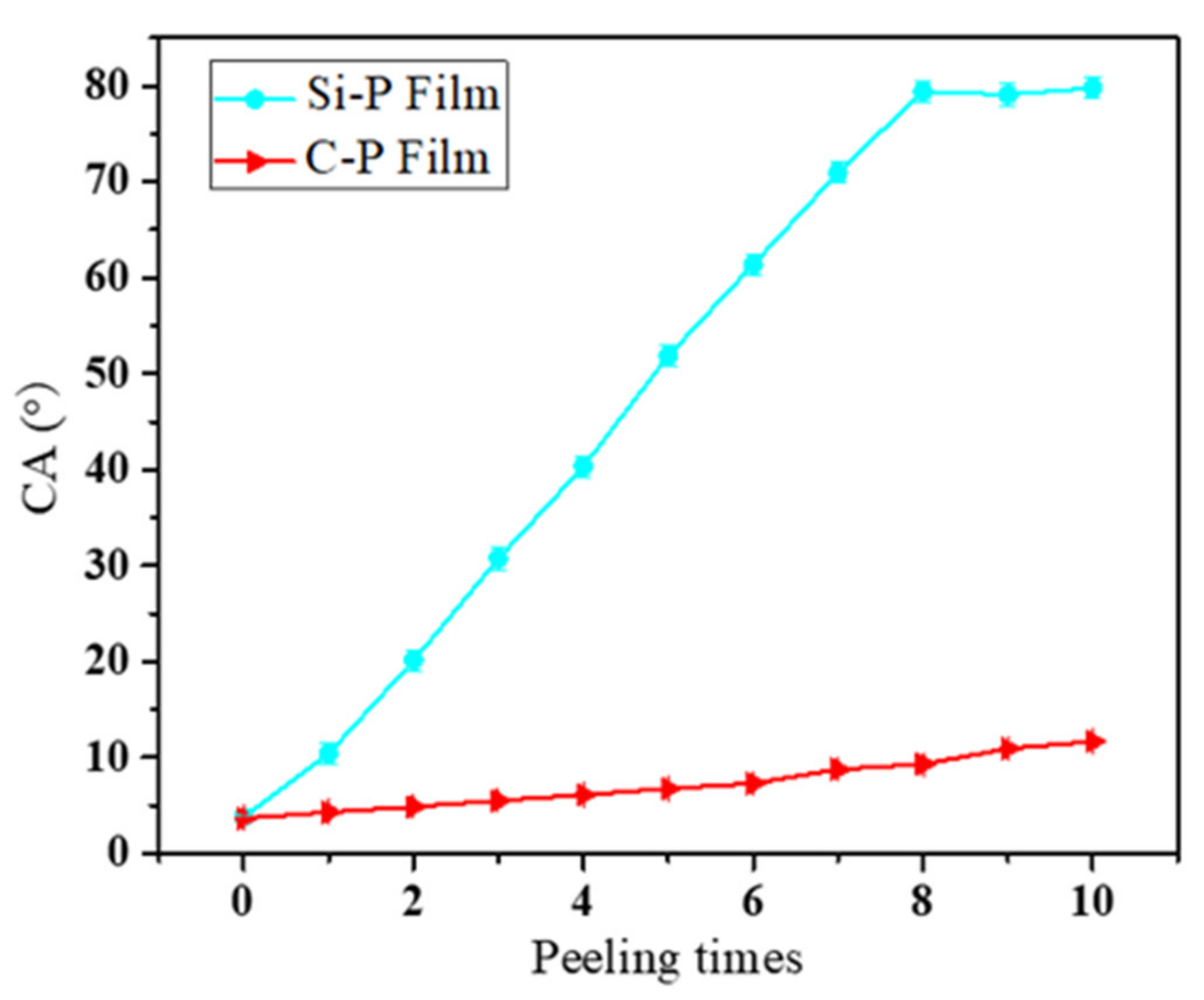
Finally, the adhesion between the superhydrophilic nano-SiO
2 particles and the P-R film was investigated. In order to evaluate the contribution of KH550, the tape stripping method was used to analyze the Si-P and C-P samples, and the adhesion to the surface was also characterized by the relationship between CA and different peel times, as shown in
Figure 12. If silica sol was coated directly onto the P-R film without depositing KH550, we found that as the peeling times increased, the P-R film incline was more hydrophobic, and when the peeling numbers enlarged to 8 times, the CA of the film was basically close to 80°, which was almost the same as that of the flat PMMA. In contrast, when the KH550 grafted silica sol was sprayed on the P-R film, the average CA of the P-R film rose slightly with the augment of peeling times, even if the peeling numbers extended to 10 times, the average CA of the film slightly increased 5.65°, which indicated fully that the sprayed superhydrophilic nano-SiO
2 particles were effectively bonded to the P-R film.
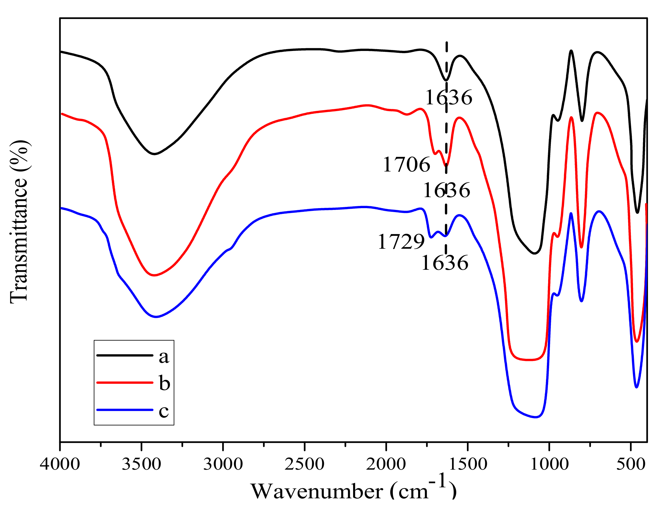
3.5. FTIR Measurement
The FTIR spectra of silica sol (a), KH550 grafted silica sol (b), and C-P film (c) are shown in
Figure 13. It can be found that there is an absorption peak at around 1636 cm
−1 for all three spectra. For spectrum b, the absorption peak at 1706 cm
−1 is due to the C=O functional group, which is not found in spectrum a. This is because the C=O functional group in KH550 forms a hydrogen bond with the hydroxyl group of silica surface, resulting in the absorption peak was shifted from 1729 cm
−1 to 1706 cm
−1. In spectrum c, the absorption peak at 1729 cm
−1 was formed as a result of the C=O functional group in PMMA, further confirming the strong chemical bonding between the PMMA film and silica, which enhances the binding force between SiO
2 nanoparticles and PMMA substrate, thus the mechanical properties of the film were improved remarkably.
4. Conclusions
In this paper, a multifunctional film with excellent mechanical properties was fabricated using polymethylmethacrylate (PMMA) as a substrate, combined with wet etching and micro-transfer printing method. In particular, the synergistic effect of inverted pyramid microstructure and SiO2 nanoparticles gives the film excellent antireflective, superhydrophilic and AF properties, in which the addition of silane coupling agent KH550 enhances the bonding performance of SiO2 nanoparticles to the substrate. The hardness of the C-P film was raised by 2.8 (HD) compared to the P-R film. The average CA of the C-P film increased insignificantly from 3.17° to 4.76° when the friction number reached 25. The average CA of the C-P film augmented somewhat, from 3.21° to 9.86°, when the number of peeling times was 10, compared with the hydrophilic nanoparticles sprayed directly on the substrate, and the average CA of the film was close to 80°, showing that the KH550 grafted silica sol was able to bind effectively with the substrate. In the visible wavelength range (400–800 nm), the average transmittance of the C-P film was 5.25% higher than that of the F-P film. After spraying the F-P, P-R and C-P films for 6 min, the average transmittance of C-P film remained at 92.26%, especially after the 100 °C water vapor test for 10 s, the C-P film still maintained its transparent and clear appearance. The above results demonstrate that the prepared film possesses excellent AF performance, and the film was expected to be used in the field of optics in different types of lenses, from personal and sports eyewear to transparent displays and sensors, etc.
Author Contributions
Conceptualization, S.N., G.T.; data curation, S.N.; formal analysis, X.F.; funding acquisition, X.F., G.T.; investigation, H.Z.; methodology, S.N.; project administration, X.F.; supervision, G.T.; validation, X.F., H.Z.; visualization, H.Z., G.T.; writing—original draft preparation, X.F.; writing—review and editing, S.N., G.T. All authors have read and agreed to the published version of the manuscript.
Funding
This work is supported by the National Natural Science Foundation of China (No. 52005227), the Natural Science Research Project of Jiangsu Province University (No. 20KJB410003) and the Opening Project of the Key Laboratory of Bionic Engineering (Ministry of Education), Jilin University (No. KF20200007).
Institutional Review Board Statement
Not applicable.
Informed Consent Statement
Not applicable.
Data Availability Statement
The study did not report any data.
Conflicts of Interest
The authors declare no conflict of interest.
References
- Carlisi, C.; Trepci, E.; Li, X.; Sakkaf, R.A.; Palmisano, G. Multilayer thin film structures for multifunctional glass: Self-cleaning, antireflective and energy-saving properties. Appl. Energy 2020, 264, 114697. [Google Scholar] [CrossRef]
- Yuan, J.; Yan, S.; Xiao, Z.; Hu, J. Multifunctional closed-pore silica/titania composite antireflective coatings based on self-assembly process. Mater. Chem. Phys. 2020, 250, 123023. [Google Scholar] [CrossRef]
- Zhang, S.; Zhang, J.; Zhu, B.; Niu, S.; Han, Z.; Ren, L. Progress in bio-inspired anti-solid particle erosion materials: Learning from nature but going beyond nature. Chin. J. Mech. Eng. 2020, 33, 42. [Google Scholar] [CrossRef]
- Wei, G.; Yang, D.; Zhang, T.; Yue, X.; Qiu, F. Fabrication of multifunctional coating with high luminous transmittance, self-cleaning and radiative cooling performances for energy-efficient windows. Sol. Energy Mater. Sol. Cells. 2019, 202, 110125. [Google Scholar] [CrossRef]
- Han, Z.; Wang, Z.; Li, B.; Feng, X.; Jiao, Z.; Zhang, J.; Zhao, J.; Niu, S.; Ren, L. Flexible self-cleaning broadband antireflective film inspired by the transparent cicada wings. ACS Appl. Mater. Interfaces 2019, 11, 17019. [Google Scholar] [CrossRef] [PubMed]
- Mozumder, M.S.; Mourad, A.H.I.; Pervez, H.; Surkatti, R. Recent developments in multifunctional coatings for solar panel applications: A review. Sol. Energy Mater. Sol. Cells. 2019, 189, 75–102. [Google Scholar] [CrossRef]
- Motamedi, M.; Warkiani, M.E.; Taylor, R.A. Transparent surfaces inspired by nature. Adv. Opt. Mater. 2018, 6, 1800091. [Google Scholar] [CrossRef]
- Ai, L.; Zhang, J.; Li, X.; Lu, Y.; Song, W. Universal low-temperature process for preparation of multifunctional high-performance antireflective mesoporous silica coatings on transparent polymeric substrates. ACS Appl. Mater. Interfaces 2018, 10, 4993. [Google Scholar] [CrossRef]
- Kasar, A.K.; Menezes, P.L. Surface engineering of solar cells to improve efficiency. JOM 2019, 71, 4319. [Google Scholar] [CrossRef]
- Luo, X.; Lu, L.; Yin, M.; Fang, X.; Chen, X.; Li, D.; Yang, L.; Li, G.; Ma, J. Antireflective and self-cleaning glass with robust moth-eye surface nanostructures for photovoltaic utilization. Mater. Res. Bull. 2018, 109, 183–189. [Google Scholar] [CrossRef]
- Zada, I.; Zhang, W.; Sun, P.; Imtiaz, M.; Abbas, W.; Zhang, D. Multifunctional, angle dependent antireflection, and hydrophilic properties of SiO2 inspired by nano-scale structures of cicada wings. Appl. Phys. Lett. 2017, 111, 153701. [Google Scholar] [CrossRef]
- Park, S.; Moon, H. Antifogging, antireflective, and highly transparent coatings fabricated with SiO2 and TiO2 nanoparticles. Sci. Adv. Mater. 2017, 9, 1560–1565. [Google Scholar] [CrossRef]
- Tao, H.; Zhang, W.; Zhang, C.; Han, L.; Wang, J.; Tan, B.; Li, Y.; Kan, C. High absorption perovskite solar cell with optical coupling structure. Opt. Commun. 2019, 443, 262. [Google Scholar] [CrossRef]
- Ahn, S.; Iftiquar, S.M.; Cho, J.; Le, A.H.T.; Park, C.; Park, J.; Lee, H.; Hong, K.; Kim, J.S.; Bong, S.; et al. Enhancing light absorption in a thin film silicon tandem solar cell fabricated on a reactive ion etched nano-structured glass surface. J. Phys. D Appl. Phys. 2018, 52, 035502. [Google Scholar] [CrossRef]
- Tao, C.; Zhang, L. Fabrication of multifunctional closed-surface SiO2-TiO2 antireflective thin films. Colloids Surf. A 2019, 585, 124045. [Google Scholar] [CrossRef]
- Yang, D.; Zhang, T.; Wang, C.; Yu, T.; Xu, Z. Enhanced electro-optical properties of TiO2 nanocone arrays for ultrathin GaAs solar cells. Opt. Commun. 2019, 452, 281. [Google Scholar] [CrossRef]
- Khan, S.B.; Wu, H.; Huai, X.; Zou, S.; Liu, Y.; Zhang, Z. Mechanically robust antireflective coatings. Nano Res. 2018, 11, 1699–1713. [Google Scholar] [CrossRef]
- Yoon, J.; Ryu, M.; Kim, H.; Ahn, G.O.; Lee, H. Wet-style superhydrophobic antifogging coatings for optical sensors. Adv. Mater. 2020, 32, 2002710. [Google Scholar] [CrossRef]
- Han, K.M.; Yoo, J.S. Wet-texturing process for a thin crystalline silicon solar cell at low cost with high efficiency. J. Korean Phys. Soc. 2014, 64, 1132–1137. [Google Scholar] [CrossRef]
- Mueller, F.A.; Kunz, C.; Graef, S. Bio-inspired functional surfaces based on laser-induced periodic surface structures. Materials 2016, 9, 476. [Google Scholar] [CrossRef]
- Sherif, H.A.; Almufadi, F.A. Polymer modulus of elasticity and hardness from impact data. J. Eng. Mater. Technol. 2018, 141, 011010. [Google Scholar] [CrossRef]
- Wei, H.; Kuo, C.; Jaing, C.; Chang, Y.; Lee, C. Highly transparent superhydrophobic thin film with low refractive index prepared by one-step coating of modi-fied silica nanoparticles. J. Sol.-Gel. Sci. Technol. 2014, 71, 168–175. [Google Scholar] [CrossRef]
- Park, C.; Choi, B. Enhanced light extraction from bottom emission OLEDs by high refractive index nanoparticle scattering layer. Nanomaterials 2019, 9, 1241. [Google Scholar] [CrossRef] [PubMed] [Green Version]
- Xie, S.; Wan, X.; Yang, B.; Zhang, W.; Wei, X.; Zhuang, S. Design and fabrication of wafer-level microlens array with moth-eye antireflective nanostructures. Nanomaterials 2019, 9, 747. [Google Scholar] [CrossRef] [Green Version]
- Alhallak, L.; Tirkes, S.; Tayfun, U. Mechanical, thermal, melt-flow and morphological characterizations of bentonite-filled ABS copolymer. Rapid Prototyp. J. 2020, 26, 1305–1312. [Google Scholar] [CrossRef]
| Publisher’s Note: MDPI stays neutral with regard to jurisdictional claims in published maps and institutional affiliations. |
© 2021 by the authors. Licensee MDPI, Basel, Switzerland. This article is an open access article distributed under the terms and conditions of the Creative Commons Attribution (CC BY) license (https://creativecommons.org/licenses/by/4.0/).


