Article

Silicon Carbide Wafer Machining by Using a Single Filament Plasma at Atmospheric Pressure

Division of Convergence Technology, Korea Institute of Fusion Energy, 37 Dongjangsan-ro, Gunsan 54004, Korea
*
Author to whom correspondence should be addressed.
Coatings 2021, 11(8), 958; https://doi.org/10.3390/coatings11080958
Submission received: 15 July 2021 / Revised: 4 August 2021 / Accepted: 8 August 2021 / Published: 11 August 2021
(This article belongs to the Special Issue Surface Modification by Plasma-Based Processes)

Abstract

:
SiC wafers were etched using a filament plasma of He:NF3:O2 (helium:nitrogen trifluoride:oxygen) mixed gas at atmospheric pressure. When 0.5–2 sccm of NF3 was mixed to 2 slm of He filament plasma, the etch depth and etch rate increased, but there was little change in the etch width as the NF3 mixing amount increased. The increment of the NF3 mixing also suppressed the surface roughening of plasma etching. The addition of O2 to the He-NF3 filament plasma slightly increased the SiC wafer etch rate. When the NF3 mixing amount was 2 sccm, the roughness of the etched surface increased sharply by O2 addition. On the contrary, the NF3 mixing amount was 1 sccm; the addition of O2 reduced the roughness more than that of the pristine. The roughness of the pristine SiC wafer specimens is in the range of Ra 0.7–0.8 nm. After 30 min of etching on a 6 mm by 6 mm square area, the roughness of the etched surface reduced to Ra 0.587 nm, while the etch rate was 2.74 μm/h with a He:NF3:O2 of 2:1:3 (slm:sccm:sccm) filament plasma and 3 mm/s speed of raster scan etch of the optimized roughening suppression etching recipe.

1. Introduction

The silicon carbide (SiC) material is used for the mirrors of space telescopes and molds for glass optics manufacturing, due to the superb characteristics of high hardness, chemical inertness, and its low specific gravity [1,2,3]. As a result of its high hardness, it is not easily damaged by external scratches and has high thermal conductivity with low thermal expansion; therefore, it is the most suitable material for space telescopes that have to withstand extreme environments that deform or distort the optical component by high range of temperature change [4,5,6,7,8]. In addition, many studies are being conducted for using the material for high power semiconductor devices due to its wide bandgap and excellent thermal stability [9,10,11].
However, SiC has a high covalent bond/ionic bond ratio of 9:1, and for this reason, thermal deformation is very small but very brittle. In addition, the Young’s modulus/Vickers hardness and tensile strength/shear strength ratio are about 20 and 1.5, and those are very low comparing with metals of about 250 and 10, respectively. For these reasons, it is very hard to apply the conventional metal machining method for SiC material [8]. Presently, conventional machining methods such as grinding, lapping, and chemical mechanical polishing (CMP) are used for manufacturing the SiC mirror, but it takes enormous time and energy, leaving lots of surface damages such as scratches, subsurface damage (SSD), and micro pits by the machining tools, which has an adverse effect on the telescope performance [12,13,14,15,16,17,18]. In addition, for ensuring higher mirror performance, it is necessary to machine a free-form aspherical surface beyond the spherical shape. Due to the need for the free-form machining, the existing methods require a lot of time-consuming additional correction machining.
Since the SSD generation continues to occur even during the correction machining, methods using plasma that do not require direct contact with machining tools have been studied and developed. An ion beam figuring (IBF) method, which controls the roughness and shape of the target surface by injecting high-energy ions onto the surface of the material [19,20,21,22], and a reactive ion etching (RIE) method, which uses ions or radicals activated by plasma to remove the solid substrate atoms [23,24,25,26,27], have been studied to apply for the machining of SiC material. Both IBF and RIE must be performed in a vacuum environment, and it is quite cumbersome for aspherical mirror manufacturing, where inspection and machining are repeated during the manufacturing process.
As a solution for this problem, the methods using atmospheric pressure plasma (APP) have been studied on SiC mirror machining. The majority of the APP generating source for SiC material machining is a dielectric barrier discharge (DBD) plasma source. One major method for SiC machining using DBD uses the ionizing wave injected by the plasma generating gas flow on to the SiC surface [28,29,30,31]. Another DBD using method is direct discharge SiC machining, in which the SiC substrate acts as one of the DBD plasma generating electrodes, making direct contact with the processing plasma [32,33,34,35,36,37]. Since these methods can effectively control the etching width, depth, and volume removal rate, it can be a suitable tool for correction machining, which removes the part deviating from the target shape after an elemental process.
The study introduced in this report is about a precision SiC machining method using APP, which uses a uniquely designed APP generator that is different from the APP generator reported so far.

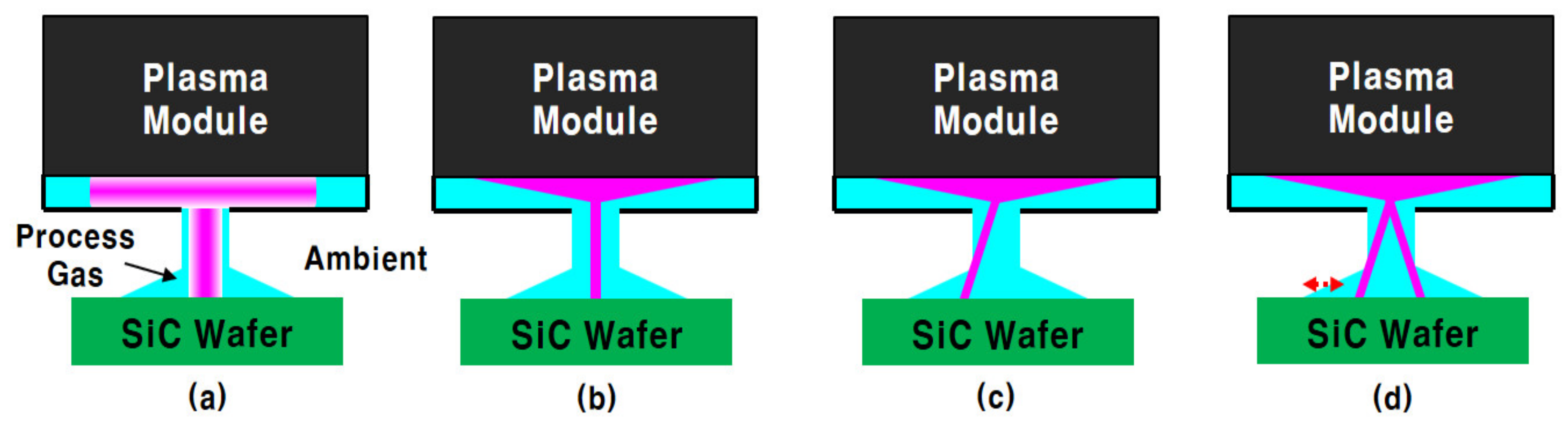
2. Materials and Methods

The plasma generation module has a DBD structure in which an annular surface DBD (ASDBD) on the corner of the alumina disk electrode and one filament plasma between the center of the alumina disk electrode and the wafer specimen are generated simultaneously. The details of the generation of the filament plasma have been described in our previous report [38]. The thickness and diameter of the alumina disk electrode are 2 mm and 20 mm, respectively. The alumina disk electrode has a circular metal coating layer with a diameter of 8 mm on its upper side, on which the plasma-generating voltage is applied. The bottom side of the alumina disk is in contact with an annular ground electrode with an inner diameter of 18 mm, and a gap of 0.2 mm formed between the annular ground electrode and a nozzle part made of PEEK constitutes the process gas-supplying slit. The diameter of the nozzle was 3 mm, and the distance between the bottom surface of the nozzle and the wafer specimen was set to 3 mm.
The power supply used for plasma generation was AP PP020-01 of EESYS (Seong Nam, Korea), which generates a bipolar pulse high voltage. In all the experiments in this paper, the voltage pulse repetition frequency was 30 kHz and the controllable output power setting was 100 W. With these output setting, the width of the pulse voltage was 3 μs, and the peak to peak voltage was 10.8 kV. Mixed gas of helium (He), nitrogen tri fluoride (NF3), and oxygen (O2) was used for the generation of the plasma, which etches SiC material.
The supply amount of the He, NF3, and O2 gas were 1–3 slm (standard liter per minute), 0.5–11 sccm (standard cubic centimeter per minute), and 0.5–4 sccm, respectively. The gas flow rate of each gas was controlled by a mass flow controller (MFC) model M3030V manufactured by Line Tech (Daejeon, Korea). The maximum flow rates that the MFCs control were 5 slm for He and 10 sccm for NF3 and O2.
A single crystal SiC wafer of 4 inches in diameter with 0.25 mm thickness manufactured by iTASCO (Seoul, Korea) was cut into a size of 15 mm × 15 mm specimen and used as an etching specimen.
The filament plasma has a large size plasma disc generated at the center of the alumina disk electrode and a small size plasma disc on the specimen surface; those are connected to each other by a branch-free straight plasma column. The SiC wafer specimen was etched by repeated moving of the filament plasma through a given moving pattern and times by the manner in Figure 1b.
The etch profile was measured using a NanoView Profiler of Nano System (Ansan, Korea), and the roughness of the etched surface was compared using a photograph obtained by irradiating a high-intensity LED light onto the specimen. The light source was LSP35FW-0034 manufactured by AItec Systems (Yokohama, Japan), which has a maximum light intensity of 33,600 Lux and a color temperature of 6500 K. The photos were taken by a Nikon D700 digital camera with a lens of focal length 60 mm and F2.8 of maximum aperture. Some specimens were analyzed by using an atomic force microscope (AFM) to acquire the precise surface roughness (Ra) data. The AFM used for the measurements was NX-10 from Park Systems (Suwon, Korea).

3. Results and Discussion

3.1. Filament Stability

The characteristics of the filament plasma generated between the plasma module and SiC wafer using He-NF3 mixed gas were examined. Depending on the amount of the gas flow rate and the composition of the He and NF3, the filament plasma has four modes as shown in Figure 2.
Figure 2a is a glow jet (GJ) discharge mode. This is a discharge mode that occurs when the mixing amount of NF3 is too low, or when a non-conductive dielectric is placed in the place of the SiC wafer in Figure 2. The SiC etching in GJ mode had a wide etching area, but the etch rate was very small and only increased the surface roughness. Figure 2b is a normal filament (NF) plasma mode. The filament plasma in NF mode is developed normally on the surface of the SiC wafer, which is suitable for the etching process. When the mixing amount of NF3 increased beyond the NF mode range, the stability of the filament channel begins to deteriorate, causing the filament channel to become crooked (crooked filament, CF) and further to a jittering filament (JF). When a larger amount of NF3 than JF mode is mixed, the voltage required to sustain the filament plasma between the alumina electrode and the surface of the SiC wafer increases above the output voltage of the power supply, and the filament plasma disappears. Table 1 shows the changes in filament plasma mode according to the amount of NF3 mixing with 1, 2, and 3 slm of He.
When the amount of NF3 supplied was more than 4 sccm with He 1 slm, the discharge mode changes to the CF mode. On the other hand, when the He gas supply amount was 2 and 3 slm, the NF mode can be sustained even at the mixing amount of 9 and 10 sccm of NF3 gas, respectively. The reason for the narrower range of NF3 mixing amount for NF mode at 1 slm of He is that the ambient air diffused into the filament area owing to the low nozzle jet velocity (2.36 m/s) made the voltage sustaining the stable filament plasma higher. However, in the case of 2 and 3 slm (nozzle jet velocity: 4.72 and 7.08 m/s, respectively) of He supply, the process gas is sufficiently transferred to the SiC surface without the diffusion of the ambient air into the filament area. In other words, if the output power (Pset) of the power supply is raised, the NF3 mixing range for NF mode can be extended.

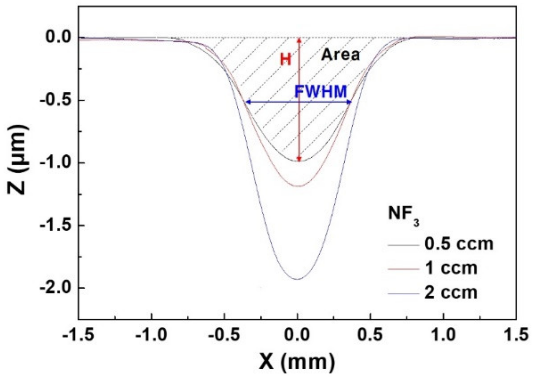
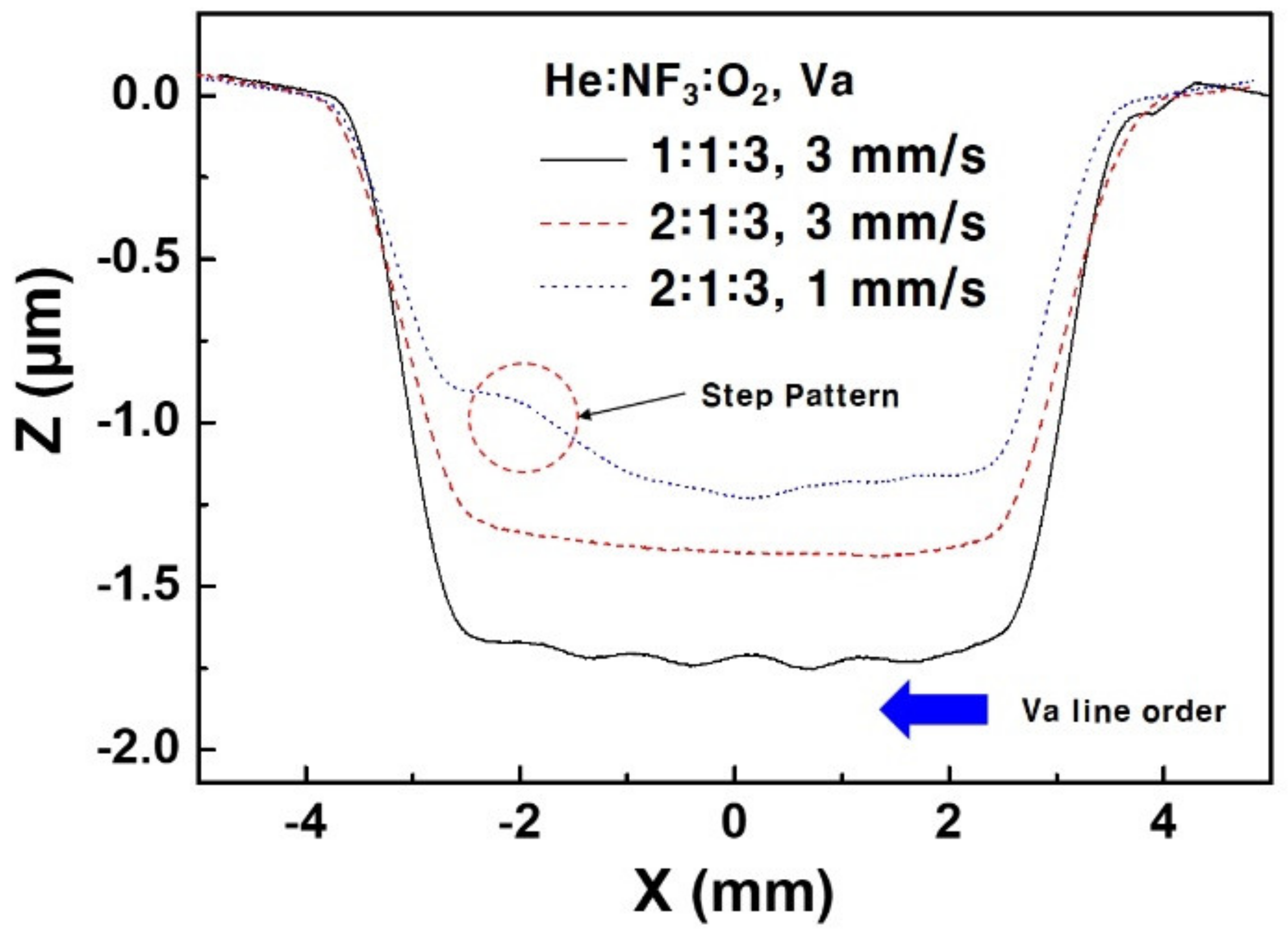
3.2. 6 mm Linear Scan Etch Profile

The etch profiles of SiC wafer specimens etched by the filament plasma of 2 slm He and 0.5, 1, 2 sccm NF3 mixed gas were checked. The main mechanisms for SiC etching in fluorine containing plasma are divided into ion bombardment etching by high-energy ions, chemical etching by fluorine radicals and atoms, ion active chemical etching, and inhibitor-controlled chemical etching [4]. In the He-NF3 mixed gas plasma at atmospheric pressure and 30kHz of low frequency voltage, it is expected that the portion of ion bombardment etching is relatively low, whereas the portion of the chemical etching is high. The reaction schemes of chemical etching of SiC material by fluorine atoms is as follows [4,29,39,40].
SiC (s) + (x+y) F (g) → SiFx (g) + CFy (g) (x, y = 1 to 4)
SiO2 (s) + xF (g) → SiFx (g) + O2 (g) (x = 1 to 4)
In the reaction schemes (Equations (1) and (2)), the letters s and g denote solid and gas state, respectively, and the letters x and y mean the numbers of fluorine atoms. Equation (1) shows a SiC removing reaction by fluorine atoms, and Equation (2) shows a reaction in which a silicon oxide film formed by contact with oxygen in the ambient air is removed by fluorine atoms [30,41].
After the filament plasma was formed on the surface of the SiC wafer specimen, the specimen surface was etched by repeated moving of the filament plasma forward and backward on a 6 mm line 80 times at a speed of 1 mm/s to make a 6 mm long etch groove. Figure 3 shows the etch profile of the perpendicular direction to the moving line in the middle of the etch groove etched by 0.5, 1, 2 sccm NF3, and 2 slm He mixed gas filament plasma. All the etch profiles showed a Gaussian profile, and the etch depth and area increased as the amount of NF3 mixing was increased. By fitting each profile with a Gaussian distribution function, the depth (H, μm), full width of half maximum (FWHM, mm), and area (Area, mm2) of the profile are obtained. Here, the volume removed by 80 linear scan etchings can be calculated by multiplication of the Area by 6 mm of the scan length. Again, the volume removal rate (VRR, mm3/h) of each filament plasma can be calculated by the total etching time of 8 min. Table 2 summarizes the Area, H, and FWHM for each filament plasma.
From the results in Table 1 and Figure 3, H and Area increased as the amount of NF3 mixing increased, but there was no significant change in FWHM. The size of the FWHM and the shape of the etch profile will be greatly affected by the size and plasma particle distribution of the plasma disc formed on the specimen surface, and the H and Area are related to the concentration of etching agent in the plasma disc. Hence, when the plasma generating electrode and the applied voltage were given, the increase in NF3 mixing amount in the range of 0.5–2 sccm into 2 slm of He does not change the size of the plasma disc and the plasma particle distribution much, while the concentration of the etching radical increases resulting in an increase in the etching amount.

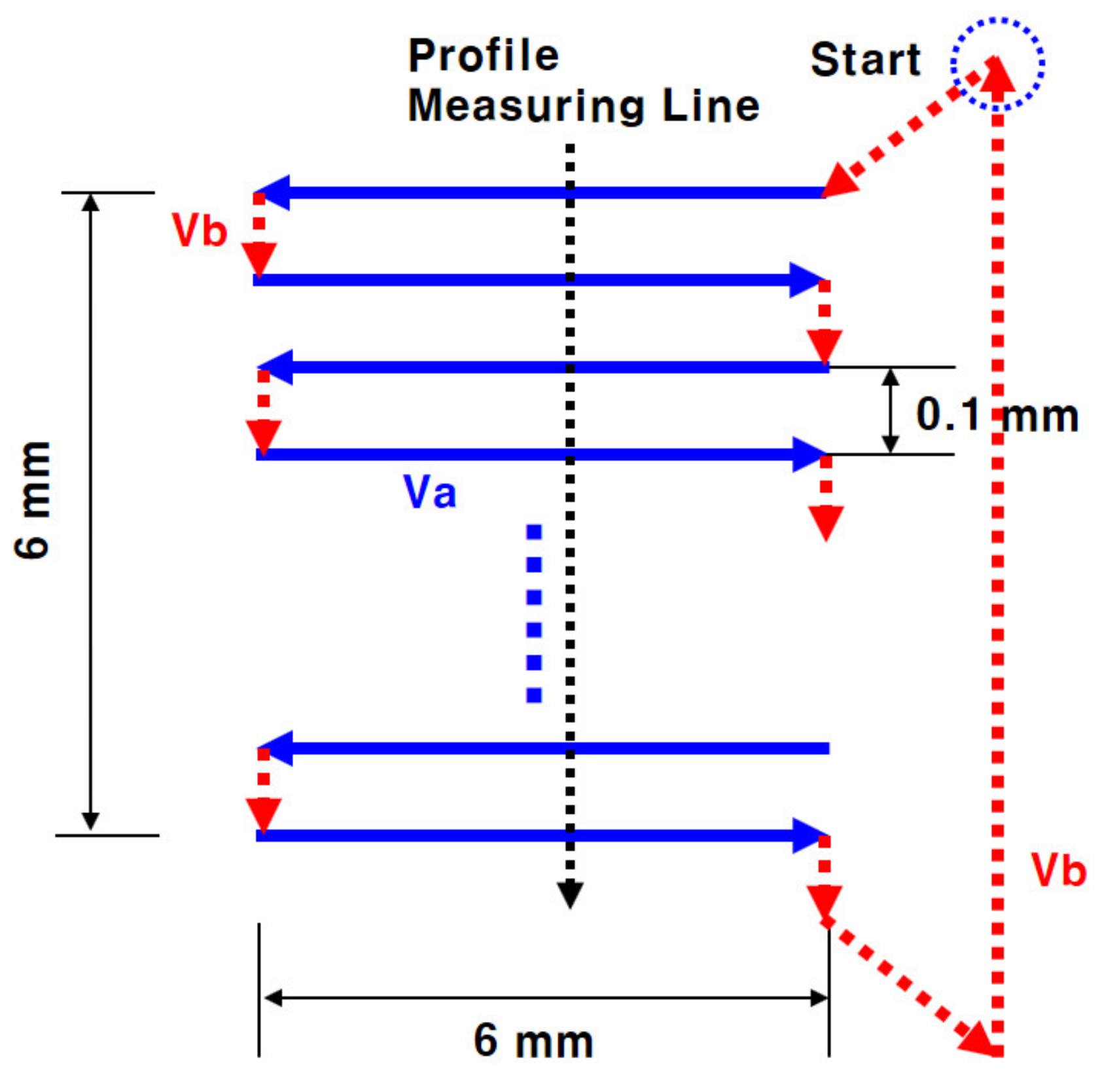
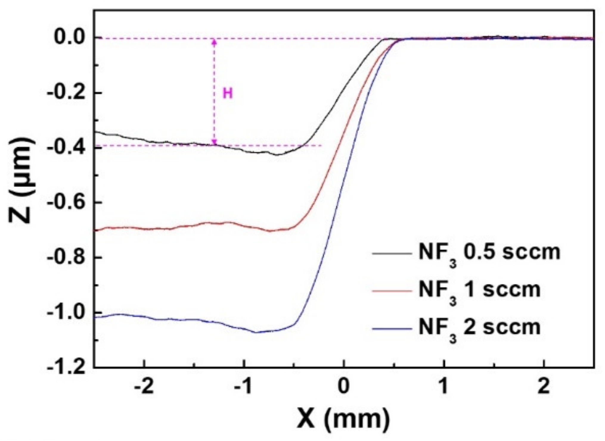
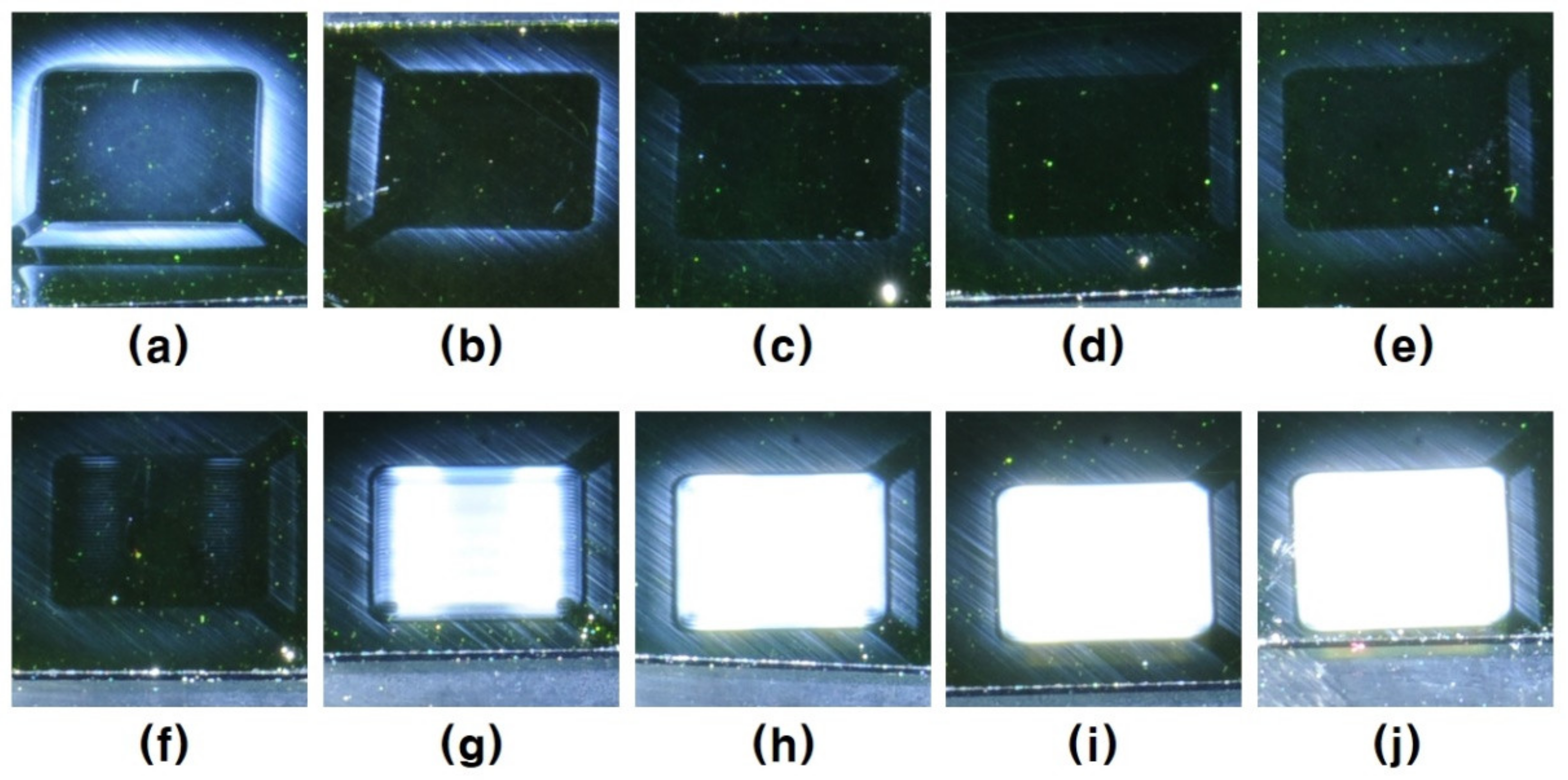
3.3. 6 by 6 mm2 Square 2D Raster Scan Etch

The plasma processing device for correction machining needs to be able to remove the part that needs some correction after the previous process as much as desired. Therefore, it is necessary to examine the applicability of not only the point or line etching but also various areas of planar shapes etching.
A precision machining experiment was performed on a 6 mm by 6 mm square area using the raster scan method. The configuration of the scanning line used in the experiment is shown in Figure 4. In Figure 4, Va is the etch scan line and Vb is the moving line of the plasma etch tool. Since the filament plasma does not disappear even in the moving line of Vb, it is necessary to maximize the Vb/Va ratio in order to minimize the amount of etching by Vb. The maximum Vb/Va of the facility used in this study is 8. We made three etched SiC wafer specimens by using a repeated raster scan five times (30 min), as shown in Figure 4 with 1 mm/s of Va, by using the three mixed gas filament plasmas shown in Figure 3.
Figure 5 shows the photographs of etched surface of the specimens. The specimen photographs in Figure 5 were taken by a digital camera with f8 of the aperture value and 2 s of the release time, as the specimens were placed under 5 cm from the 33.600 lux illumination source with a 45° angle. Although it was not perceivable with naked eyes, some haze that remained on the etched area was identified, as shown in the photographs in Figure 5. The haze that remained on the specimen surface is a result of non-uniform etching or re-deposition of etching by-products on the wafer surface during the etching process. The haze remained was strongest when the NF3 mixing was 0.5 sccm and weakest when the NF3 mixing was 2 sccm. The intensity of the haze on the etched surface is proportional to the roughness of the etched surface after etching.
To check the etch depth of each specimen, the etch profile through the line from the non-etched hill beyond the etched area of the 6 mm by 6 mm square to the center of the etched basin was measured in the direction perpendicular to the Va scan line using the NanoVIEW Profiler and shown in Figure 6. In Figure 6, it can be seen that the depth of the etching increases with little change in the etch border interface as the amount of NF3 mixing increases. Referring to the etch profile in Figure 5 and Figure 6, the etch rate increased in proportion to the amount of NF3 mixing, but the intensity of the haze that remained on the etched area was opposite to the result of the etched depth.
The main mechanisms of SiC etching using plasma can be largely divided into by ion bombardment etching and chemical etching by F atoms. Several documents report that the roughness of the etched surface increases as etching by ion bombardment dominates. The results in Figure 5 and Figure 6 are consistent with the results of the previous reports, in which the density of free F atoms increases as the amount of NF3 mixing increases, so that the etch rate is increased and the roughness of the etched surface decreases [39,42,43,44].
Figure 7 shows the photographs of specimens etched by the filament plasma of 2 slm of He and 1, 2 sccm of NF3 with the addition of O2. In several reports on RIE SiC etching, when an appropriate amount of O2 is added into the plasma of fluorine containing etchant for SiC etching, more fluorine atoms are liberated from the etchant gas species such as CxFy, SF6, and NF3; thereby, the etching rate increases. However, when an excessive amount of O2 is added, the etching rate is lowered due to the dilution effect of fluorine atoms and the formation of a silicon oxide film on the surface [4,23,24,25,43]. In addition, when the content of fluorine and oxygen particles in the plasma is increased excessively, the portion of the ion bombardment etching is increased by elevation of the self-bias on the substrate while the portion of the chemical etching is lowered. Therefore, the surface roughness is increased. In addition to that, because the oxidized silicon sites that have a different etch rate are formed non-uniformly on the SiC surface, the surface of the SiC roughens more during the etching process [28,29,30,41,42,43,44]. The etch depths of the specimens in Figure 7 are not presented in this report; the addition of O2 to the filament plasma into both cases of 1 and 2 sccm of NF3 mixing increased the etch depth by the range of 10–20%, which is consistent with the results of the previous RIE literature as for the effect of oxygen on the SiC etch rate. However, for the surface roughness change, it showed somewhat different results.
In the plasma of 1 sccm NF3 mixing, the remained haze intensity was reduced as the O2 mixing increased from 1 to 3 sccm, but the 4 sccm of O2 mixing specimen showed little rougher surface than the 3 sccm specimen. On the contrary, in the plasma in which 2 sccm of NF3 was mixed, stronger haze remained on the etched area than any other specimens of 1 sccm NF3 mixing specimens even by only 1 sccm of O2 mixing, and the remained haze was getting stronger as the amount of O2 was increased. In 1 sccm of NF3 mixing filament plasma, the O2 addition suppresses the portion of ion bombardment etching and activates the chemical etching more. However, when 4 sccm of O2 was mixed, the portion of ion bombardment etching starts to increase considerably. So, the remained haze starts to increase again. Every position in the etch area meets the plasma disc five times during the whole etch process, as previously stated. Therefore, it increases after the filament plasma without O2 addition passed one position on the SiC specimen surface once, which exposes the carbon-rich surface to contact with ambient air [44]. At this moment, the oxygen in the air makes an oxidized site on the specimen surface not uniformly. When the surface that has the non-uniform oxidized site enters the plasma region again, this non-uniform oxidized site prevents the uniform and smooth etching and leaves haze on the etched surface. The filament plasma with the addition of an appropriate amount of O2 leaves a silicon-rich surface and uniform oxidized site on the specimen surface, so that the roughening by plasma etch can be suppressed more [30,31,44]. However, in the filament plasma of 2 sccm of NF3 mixing, even by the addition of only 1 sccm of O2, fluorine radical and oxygen atoms are excessively liberated in the plasma, increasing not only self bias, which enhances the ion bombardment etching but also the chemical etching. As a result, it seems that the high level of ion bombardment etching, the re-deposition of ion bombardment etching by-products, and also the high level of chemical etching results in the extremely rough surface of the etched area.

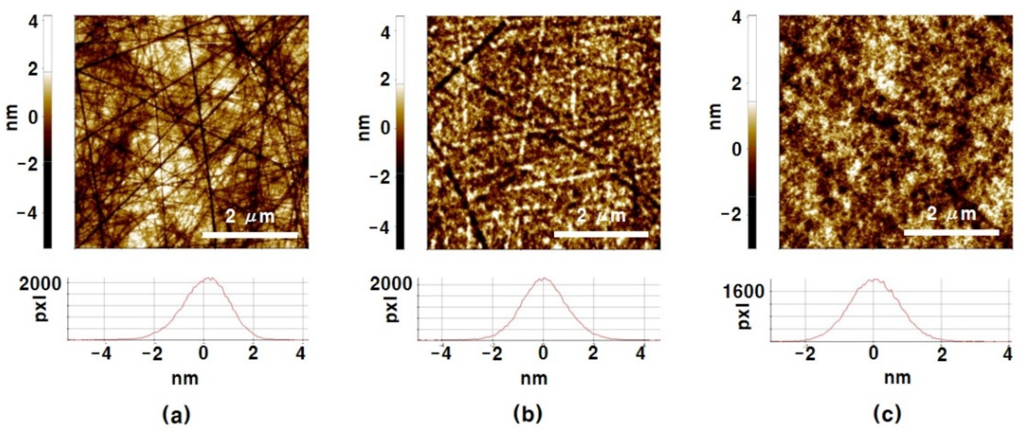
3.4. Profile Stability and Roughness Reduction

Figure 8 shows the etch profiles of specimens etched by He:F3:O2 2:1:3 (slm:sccm:sccm, omitted after) filament plasma for 30 min with the Va of 1 and 3 mm/s and He:NF3:O2 1:1:3 with Va of 3 mm/s. The etched area was 6 mm by 6 mm square, and the raster scan pattern of Figure 4 was used for all the three specimens. The repetition times passing the whole raster scan pattern of Figure 4 with 1 and 3 mm/s of Va for 30 min are 5 and 15, respectively.
It takes 6 min to scan all the raster scan patterns of the 6 mm by 6 mm square area once with 1 mm/s of Va and a scan line pitch of 0.1 mm. After a certain period of time has elapsed since contact with the filament plasma, the temperature of the 15 mm by 15 mm, 0.25 mm thickness of SiC wafer specimen is stabilized at slightly elevated temperature. If the temperature of the specimen stabilized before the first scan completed, it makes the bottom profile uneven due to the different etch rate by the specimen temperature difference. These facts are the reason for the uneven bottom profile of the etch specimen of He:NF3:O2 2:1:3 with Va 1 mm/s, as shown in Figure 8.
The bottom profile of the specimen of He:NF3:O2 1:1:3 of reduced He amount with Va 3 mm/s in Figure 8 shows the wave pattern. In this filament plasma, the NF3 concentration was the highest; hence, the etch depth was deepest. However, due to the lower nozzle jet velocity, external air is diffused into the filament plasma area, which increases the filament plasma sustaining voltage. The change in the filament-sustaining voltage influences the output voltage of the power supply, which actively control the output power to keep the setting power of 100 W. It forms a waved bottom profile.
The problems of this deterioration of etching profile stability were solved by the following means: first, increasing Va from 1 to 3 mm/s to minimize the effect of temperature change during the first scan, and second, prevention of the inflow of ambient air into the filament plasma by supplying He of more than 2 slm or setting the Pset higher rather than change its output voltage.
By application of these solutions, the etch profile of the specimen of He:NF3:O2 2:1:3 with Va 3 mm/s in Figure 8 showed a very stable even bottom profile.
The surface roughness of the specimens etched with Va at 3 mm/s and the process gas with He:NF3:O2 1:1:3 and 2:1:3 in Figure 8 were measured precisely by AFM, and the results are represented in Figure 9. Figure 9a is the AFM result of a primitive SiC wafer. A large amount of tool scratches remained in the final polishing process when the specimen manufacturer produced the wafer were observed. The measured surface roughness of the pristine SiC wafer specimen was Ra 0.749 nm. The etch depth of the 6 mm by 6 mm etched area by He:NF3:O2 1:1:3 filament plasma for 30 min was 1.72 μm. The AFM result of this specimen is shown in Figure 9b. The scratches on the surface of the SiC specimen shown in the pristine specimen were slightly removed, and the Ra was also slightly reduced to 0.732 nm. The process conditions that showed the best haze suppression and profile stability in the results of Figure 7 and Figure 8 were He:NF3:O2 2:1:3 with Va 3 mm/s. The etch depth of the specimen etched by this optimized process condition for 30 min was 1.37 μm. Although the etch rate was slightly lower than by the He:NF3:O2 1:1:3 filament plasma, as shown in Figure 9c, the tool scratches shown on the pristine wafer were completely removed, and the measured roughness was Ra 0.587 nm, which was rather smoother than the pristine.

4. Conclusions

A He filament plasma with a single plasma column was formed between a SiC wafer surface and an annular surface discharge with a dielectric barrier discharge plasma source (ASDBD), and a small amount of NF3 and O2 was mixed to etch the SiC wafer. The He filament plasma tends to become unstable as the mixing amount of NF3 increases, because the higher concentration of NF3 in the filament plasma increases the voltage for the stable filament plasma sustention than the supplying voltage.
In the etch profile of the SiC wafer etched by the filament plasma of mixed gas of 0.5–2 sccm of NF3 and 2 slm of He, as the mixing amount of NF3 increased, the etch rate increased, but there was no significant change in the etch width.
The He-NF3 mixed gas filament plasma etching leaves some haze, i.e., the surface roughness by the plasma etching, on the etched surface. The increment of NF3 mixing decreases the remained haze intensity, while the etch rate increases. The haze remained on the etched surface mainly due to the increment of the portion of the ion bombardment etching having a higher rate of re-deposition of the etch by-product and the generation of the non-uniform oxide site on the specimen surface to be etched repeatedly.
The addition of an optimized amount of oxygen to the He:NF3 2:1 (slm:sccm) filament plasma liberates fluorine atoms from NF3 molecules more, which increases the portion of the chemical etching compared to ion bombardment etching and makes the oxide site on the surface etched uniformly. For these reasons, the roughening effect by the plasma etching can be suppressed. However, when an excessive amount of NF3 and O2 were mixed to the filament plasma, the chemical etching and ion bombardment etching increased simultaneously; thereby, the roughness of the etched surface increases greatly. The etch rate by the optimized etch condition for suppression of the surface roughening was 2.74 μm/h for a 6 mm by 6 mm square area. After 30 min of etching on the square area, the roughness of the etched surface was Ra 0.587 nm, and the roughness of the pristine SiC wafer specimens was in the range of Ra 0.7–0.8 nm.

Author Contributions

Conceptualization, Y.S.C. and D.C.S.; methodology, D.C.S. and K.I.L.; validation, S.Y. and Y.H.J.; investigation, Y.H.J., S.Y., and D.C.S.; data curation, D.C.S. and K.I.L.; writing—original draft preparation, S.Y. and D.C.S.; writing—review and editing, S.Y. and D.C.S.; project administration, Y.S.C.; funding acquisition, Y.S.C. All authors have read and agreed to the published version of the manuscript.

Funding

This research was supported by R&D Program of “Plasma Convergence & Fundamental Research Project [code No. (EN-2021)-1711124796]” through the Korea Institute of Fusion Energy (KFE) funded by the Government funds, Republic of Korea.

Institutional Review Board Statement

Not applicable.

Informed Consent Statement

Not applicable.

Data Availability Statement

Not applicable.

Conflicts of Interest

The authors declare no conflict of interest.

References

  1. Casstevens, J.M.; Rashed, A.; Plummer, R.; Bray, D.; Gates, R.L.; Lara-Curzio, E.; Ferber, M.K.; Kirkland, T. Silicon carbide high performance optics: A cost-effective, flexible fabrication process. Proc. SPIE 2001, 4451, 458–467. [Google Scholar] [CrossRef]
  2. Ebizuka, N.; Dai, Y.; Eto, H.; Lin, W.; Ebisuzaki, T.; Omori, H.; Handa, T.; Takami, H.; Takahashi, Y. Development of SiC ultra-light mirror for large space telescope and for extremely huge ground based telescope. Proc. SPIE 2003, 4842, 329–334. [Google Scholar]
  3. Hall, C.; Tricard, M.; Murakoshi, H.; Yamamoto, Y.; Kuriyama, K.; Yoko, H. New mold manufacturing techniques. Proc. SPIE 2005, 5868, 58680V. [Google Scholar] [CrossRef]
  4. Yih, P.H.; Saxena, V.; Steckl, A.J. A Review of SiC Reactive Ion Etching in Fluorinated Plasmas. Phys. Stat. Sol. (b) 1997, 202, 605–642. [Google Scholar] [CrossRef]
  5. Vassen, R.; Stöver, D. Processing and Properties of Nanograin Silicon Carbide. J. Am. Ceram. Soc. 1999, 82, 2585–2593. [Google Scholar] [CrossRef]
  6. Calvel, B. Recent development in silicon carbide lightweight optics at Matra Marconi Space. In Proceedings of the Next Generation Space Telescope Science and Technology, Hyannis, MA, USA, 13–16 September 1999; Smith, E., Long, K., Eds.; ASP Conference Series: Hyannis, MA, USA, 1999; p. 435. [Google Scholar]
  7. Johnson, J.S.; Grobsky, K.D.; Bray, D. Rapid fabrication of lightweight silicon carbide mirrors. Proc. SPIE 2002, 4771, 243–253. [Google Scholar] [CrossRef]
  8. Goel, S. The current understanding on the diamond machining of silicon carbide. J. Phys. D: Appl. Phys. 2014, 47, 243001. [Google Scholar] [CrossRef] [Green Version]
  9. Dillon, J.A., Jr.; Schlier, R.E.; Farnswaorth, H.E. Some Surface Properties of Silicon-Carbide Crystals. J. Appl. Phys. 1959, 30, 675–679. [Google Scholar] [CrossRef]
  10. Bechstedt, F.; Käckell, P.; Zywietz, A.; Karch, K.; Adolph, B.; Tenelsen, K.; Furthmüller, J. Polytypism and Properties of Silicon Carbide. Phys. Stat. Sol. (b) 1997, 202, 35–62. [Google Scholar] [CrossRef]
  11. Neudeck, P. Silicon Carbide Technology; NASA Lewis Research Center: Cleveland, OH, USA, 1998. [Google Scholar]
  12. Xu, H.H.K.; Padture, N.P.; Jahanmir, S. Effect of Microstructure on Material-Removal Mechanisms and Damage Tolerance in Abrasive Machining of Silicon Carbide. J. Am. Ceram. Soc. 1995, 78, 2443–2448. [Google Scholar] [CrossRef]
  13. Zhang, B.; Zheng, X.L.; Tokura, H.; Yoshikawa, M. Grinding induced damage in ceramics. J. Mater. Proc. Technol. 2003, 132, 353–364. [Google Scholar] [CrossRef]
  14. Gao, J.; Chen, J.; Liu, G.; Yan, Y.; Liu, X.; Huang, Z. Role of microstructure on surface and subsurface damage of sintered silicon carbide during grinding and polishing. Wear 2010, 270, 88–94. [Google Scholar] [CrossRef]
  15. Murray, J.W.; Fay, M.W.; Kunieda, M.; Clare, A.T. TEM study on the electrical discharge machined surface of single-crystal silicon. J. Mater. Process. Technol. 2013, 213, 801–809. [Google Scholar] [CrossRef]
  16. Groth, B.; Haber, R.; Mann, A. Raman Micro-Spectroscopy of Polytype and Structural Changes in 6H-Silicon Carbide due to Machining. Int. J. Appl. Ceram. Technol. 2015, 12, 795–804. [Google Scholar] [CrossRef]
  17. Tan, T.H.; Yan, J. Atomic-scale characterization of subsurface damage and structural changes of single-crystal silicon carbide subjected to electrical discharge machining. Acta Mater. 2017, 123, 362–372. [Google Scholar] [CrossRef]
  18. Rao, X.; Zhang, F.; Lu, Y.; Luo, X.; Chen, F. Surface and subsurface damage of reaction-bonded silicon carbide induced by electrical discharge diamond grinding. Int. J. Mach. Tools Manuf. 2020, 154, 103564. [Google Scholar] [CrossRef]
  19. Schindler, A.; Haensel, T.; Flamm, D.; Frank, W.; Boehm, G.; Frost, F.; Fechner, R.; Bigl, F.; Rauschenbach, B. Ion Beam and Plasma Jet Etching for Optical Component Fabrication. Proc. SPIE 2001, 4440, 217–227. [Google Scholar]
  20. Frost, F.; Fechner, R.; Ziberi, B.; Flamm, D.; Schindler, A. Large area smoothing of optical surfaces by low-energy ion beams. Thin Solid Films 2004, 459, 100–105. [Google Scholar] [CrossRef]
  21. Allen, D.M.; Shore, P.; Evans, R.W.; Fanara, C.; O’Brien, W.; Marson, S.; O’Neill, W. Ion beam, focused ion beam, and plasma discharge machining. CIRP Ann. 2009, 58, 647–662. [Google Scholar] [CrossRef]
  22. Frost, F.; Fechner, R.; Ziberi, B.; Völlner, J.; Flamm, D.; Schindler, A. Large area smoothing of surfaces by ion bombardment: Fundamentals and applications. J. Phys.: Condens. Matter 2009, 21, 224026. [Google Scholar] [CrossRef]
  23. Richter, C.; Espertshuber, K.; Wagner, C.; Eickhoff, M.; Krötz, G. Rapid plasma etching of cubic Sic using NF3-O2 gas mixtures. Mater. Sci. Eng. B 1997, 46, 160–163. [Google Scholar] [CrossRef]
  24. Reichert, W.; Stefan, D.; Obermeier, E.; Wondrak, W. Fabrication of smooth β-SiC surfaces by reactive ion etching using a graphite electrode. Mater. Sci. Eng. B 1997, 46, 190–194. [Google Scholar] [CrossRef]
  25. Tanaka, S.; Rajanna, K.; Abe, T.; Esashi, M. Deep reactive ion etching of silicon carbide. J. Vac. Sci. Technol. B 2001, 19, 2173–2176. [Google Scholar] [CrossRef]
  26. Lee, H.Y.; Kim, D.W.; Sung, Y.J.; Yeom, G.Y. Characteristics of Silicon Carbide Etching Using Magnetized Inductively Coupled Plasma. Jpn. J. Appl. Phys. 2005, 44, 1445–1449. [Google Scholar] [CrossRef]
  27. Oda, H.; Wood, P.; Ogiya, H.; Miyoshi, S.; Tsuji, O. Optimizing the SiC Plasma Etching Process for Manufacturing Power Devices. In Proceedings of the CS MANTECH Conference 2015, Scottsdale, AZ, USA, 18–21 May 2015; pp. 125–128. [Google Scholar]
  28. Eichentopf, I.-M.; Böhm, G.; Arnold, T. Etching mechanisms during plasma jet machining of silicon carbide. Surf. Coat. Tech. 2011, 205, S430–S434. [Google Scholar] [CrossRef]
  29. Arnold, T.; Böhm, G. Application of atmospheric plasma jet machining (PJM) for effective surface figuring of SiC. Precis. Eng. 2012, 36, 546–553. [Google Scholar] [CrossRef]
  30. Deng, H.; Endo, K.; Yamamura, K. Damage-free finishing of CVD-SiC by a combination of dry plasma etching and plasma-assisted polishing. Int. J. Mach. Tools Manuf. 2017, 115, 38–46. [Google Scholar] [CrossRef]
  31. Sun, R.; Yang, X.; Ohkubo, Y.; Endo, K.; Yamamura, K. Optimization of Gas Composition Used in Plasma Chemical Vaporization Machining for Figuring of Reaction-Sintered Silicon Carbide with Low Surface Roughness. Sci. Rep. 2018, 8, 2376. [Google Scholar] [CrossRef]
  32. Arnold, T.; Böhm, G.; Fechner, R.; Meister, J.; Nickel, A.; Frost, F.; Hänsel, T.; Schindler, A. Ultra-precision surface finishing by ionbeam and plasma jet techniques—status and outlook. Nucl. Instrum. Methods Phys. Res. A 2010, 616, 147–156. [Google Scholar] [CrossRef]
  33. Sano, Y.; Kato, T.; Yamamura, K.; Mimura, H.; Matsuyama, S.; Yamauchi, K. Beveling of Silicon Carbide Wafer by Plasma Etching Using Atmospheric-Pressure Plasma. Jpn. J. Appl. Phys. 2010, 49, 08JJ03. [Google Scholar] [CrossRef]
  34. Watanabe, H.; Ohmi, H.; Kakiuchi, H.; Hosoi, T.; Shimura, T.; Yasutake, K. Surface cleaning and etching of 4H-SiC(0001) using high-density atmospheric pressure hydrogen plasma. J. Nanosci. Nanotechnol. 2011, 11, 2802–2808. [Google Scholar] [CrossRef] [PubMed]
  35. Yamamura, K.; Yamamoto, Y.; Deng, H. Preliminary Study on Chemical Figuring and Finishing of Sintered SiC Substrate Using Atmospheric Pressure Plasma. Procedia CIRP 2012, 3, 335–339. [Google Scholar] [CrossRef] [Green Version]
  36. Sano, Y.; Aida, K.; Kato, T.; Yamamura, K.; Mimura, H.; Matsuyama, S.; Yamauchi, K. Cutting of SiC Wafer by Atmospheric-Pressure Plasma Etching with Wire Electrode. Mater. Sci. Forum 2012, 717, 865–868. [Google Scholar] [CrossRef]
  37. Sano, Y.; Nishikawa, H.; Okada, Y.; Yamamura, K.; Matsuyama, S.; Yamauchi, K. Dicing of SiC wafer by atmospheric-pressure plasma etching process with slit mask for plasma confinement. Mater. Sci. Forum 2014, 724, 759–762. [Google Scholar] [CrossRef]
  38. Seok, D.C.; Yoo, S.R.; Lee, K.I.; Choi, Y.S.; Jung, Y.H. Relation between etching profile and voltage–current shape of sintered SiC etching by atmospheric pressure plasma. Plasma Sci. Technol. 2019, 21, 045504. [Google Scholar] [CrossRef]
  39. Habuka, H.; Oda, S.; Fukai, Y.; Fukae, K.; Takeuchi, T.; Aihara, M. Silicon Carbide Etching Using Chlorine Trifluoride Gas. Jpn. J. Appl. Phys. 2005, 44, 1376–1381. [Google Scholar] [CrossRef]
  40. Shioda, K.; Kurashima, K.; Habuka, H.; Ito, H.; Mitani, S.; Takahashic, Y. Quick Cleaning Process for Silicon Carbide Chemical Vapor Deposition Reactor. ECS J. Solid State Sci. Technol. 2017, 6, 526–530. [Google Scholar] [CrossRef] [Green Version]
  41. Costello, J.A.; Tressler, R.E. Oxidation Kinetics of Silicon Carbide Crystals and Ceramics I, In Dry Oxygen. J. Am. Ceram. Soc. 1986, 69, 674–681. [Google Scholar] [CrossRef]
  42. Kim, B.; Kim, K.; Lee, B.T. Radio frequency bias power effect on surface roughness of silicon carbide plasma etching. Appl. Surf. Sci. 2003, 217, 261–267. [Google Scholar] [CrossRef]
  43. Xia, J.H.; Rusli; Choy, S.F.; Gopalakrishan, R.; Tin, C.C.; Yoon, S.F.; Ahn, J. CHF3–O2 reactive ion etching of 4H-SiC and the role of oxygen. Microelectron. Eng. 2006, 83, 381–386. [Google Scholar] [CrossRef]
  44. Xia, J.H.; Rusli; Choy, S.F.; Gopalakrishan, R.; Tin, C.C.; Ahn, J. The role of oxygen in electron cyclotron resonance etching of silicon carbide. Microelectro. Eng. 2006, 83, 9–11. [Google Scholar] [CrossRef]
Figure 1. The experimental configuration (a) and the method of etch groove making (b).
Coatings 11 00958 g001
Figure 2. Filament plasma modes of (a) glow jet (GJ), (b) normal filament (NF), (c) crooked filament (CF), and (d) jittering filament (JF).
Coatings 11 00958 g002
Figure 3. Etch profiles of SiC wafer specimens etched on 6 mm line with He 2 slm and NF3 0.5, 1, 2 sccm mixed gas filament plasma. (Pset: 100 W, tool moving speed: 1 mm/s, 80 times).
Coatings 11 00958 g003
Figure 4. The 6 mm by 6 mm raster scan etch pattern and the profile measuring line (Vb = 8·Vb).
Coatings 11 00958 g004
Figure 5. Haze on the specimen surface that remained after five times repeated etching of a 6 mm by 6 mm raster scan etch by the mixed gas filament plasma of He 2 slm and NF3 (a) 0.5 sccm, (b) 1 sccm and (c) 2 sccm. (Va: 1 mm/s).
Coatings 11 00958 g005
Figure 6. Etch profiles of the specimens etched by the mixed gas filament plasma of He 2 slm and NF3 0.5, 1, and 2 sccm (black, red and blue, respectively) of 6 mm by 6 mm raster scan etch (H: etch depth).
Coatings 11 00958 g006
Figure 7. Specimen surface of 6 mm by 6 mm square area raster scan etch by the mixed gas filament plasma of He-NF3 and O2. (ae) NF3 1 sccm, (fj) NF3 2 sccm, (a,f) O2 0 sccm, (b,g) O2 1 sccm, (c,h) O2 2 sccm, (d,i) O2 3 sccm, (e,j) O2 4 sccm.
Coatings 11 00958 g007
Figure 8. Etch profile stability comparison, black solid: He:NF3:O2 1:1:3 (slm:sccm:sccm), Va 3 mm/s, red dash: 2:1:3, Va 3 mm/s, blue dot: 2:1:3, Va 1 mm/s.
Coatings 11 00958 g008
Figure 9. AFM results of the pristine and the etched SiC wafer surface. (a) The pristine SiC wafer and the etched wafer by the mixed gas filament plasma of He:NF3:O2 (b) 1:1:3 and (c) 2:1:3 (slm:sccm:sccm) of 15 times of 6 mm by 6 mm raster scan etch at Va: 3 mm/s.
Coatings 11 00958 g009
Table 1. Filament plasma modes by He:NF3 composition change at 100 W (Pset) of applied power.
He (slm)NF3 (sccm)
0.51345691011
1NFNFNFCFCFJFnanana
2NFNFNFNFNFNFNFCFJF
3NFNFNFNFNFNFNFNFCF
Table 2. Etch profile parameters of the specimens in Figure 3.
NF3 (sccm)Area (mm2)VRR (mm3/h)H (μm)FWHM (mm)
0.57.75 × 10−43.49 × 10−21.010.72
18.32 × 10−43.75 × 10−21.210.65
213.1 × 10−45.90 × 10−22.020.61
Publisher’s Note: MDPI stays neutral with regard to jurisdictional claims in published maps and institutional affiliations.

