Article

A Numerical Investigation on the Combined Effects of MoSe2 Interface Layer and Graded Bandgap Absorber in CIGS Thin Film Solar Cells

by
Fazliyana Izzati Za’abar
1,*,
Yulisa Yusoff
2,*,
Hassan Mohamed
2,*,
Siti Fazlili Abdullah
3,
Ahmad Wafi Mahmood Zuhdi
2,
Nowshad Amin
2,
Puvaneswaran Chelvanathan
4,5,
Mohd. Shaparuddin Bahrudin
1,
Kazi Sajedur Rahman
4,
Nurul Asma Samsudin
2 and
Wan Syakirah Wan Abdullah
6
1
UNITEN R&D Sdn. Bhd., Universiti Tenaga Nasional (UNITEN), Kajang 43000, Selangor, Malaysia
2
Institute of Sustainable Energy, Universiti Tenaga Nasional (UNITEN), Kajang 43000, Selangor, Malaysia
3
College of Engineering, Universiti Tenaga Nasional (UNITEN), Kajang 43000, Selangor, Malaysia
4
Solar Energy Research Institute (SERI), Universiti Kebangsaan Malaysia (UKM), Bangi 43600, Selangor, Malaysia
5
Graphene & Advanced 2D Materials Research Group (GAMRG), School of Science and Technology (SST), Sunway University, No. 5, Jalan Universiti, Petaling Jaya 47500, Selangor, Malaysia
6
TNB Renewables Sdn. Bhd. (TRe), Level 31, PJX-HM Shah Tower, 16A Persiaran Barat, Petaling Jaya 46050, Selangor, Malaysia
*
Authors to whom correspondence should be addressed.
Coatings 2021, 11(8), 930; https://doi.org/10.3390/coatings11080930
Submission received: 18 June 2021 / Revised: 16 July 2021 / Accepted: 26 July 2021 / Published: 3 August 2021
(This article belongs to the Special Issue Achievements and Challenges in Thin Film Solar Cells)

Abstract

:
The influence of Molybdenum diselenide (MoSe2) as an interfacial layer between Cu(In,Ga)Se2 (CIGS) absorber layer and Molybdenum (Mo) back contact in a conventional CIGS thin-film solar cell was investigated numerically using SCAPS-1D (a Solar Cell Capacitance Simulator). Using graded bandgap profile of the absorber layer that consist of both back grading (BG) and front grading (FG), which is defined as double grading (DG), attribution to the variation in Ga content was studied. The key focus of this study is to explore the combinatorial effects of MoSe2 contact layer and Ga grading of the absorber to suppress carrier losses due to back contact recombination and resistance that usually occur in case of standard Mo thin films. Thickness, bandgap energy, electron affinity and carrier concentration of the MoSe2 layer were all varied to determine the best configuration for incorporating into the CIGS solar cell structure. A bandgap grading profile that offers optimum functionality in the proposed configuration with additional MoSe2 layer has also been investigated. From the overall results, CIGS solar cells with thin MoSe2 layer and high acceptor doping concentration have been found to outperform the devices without MoSe2 layer, with an increase in efficiency from 20.19% to 23.30%. The introduction of bandgap grading in the front and back interfaces of the absorber layer further improves both open-circuit voltage (VOC) and short-circuit current density (JSC), most likely due to the additional quasi-electric field beneficial for carrier collection and reduced back surface and bulk recombination. A maximum power conversion efficiency (PCE) of 28.06%, fill factor (FF) of 81.89%, JSC of 39.45 mA/cm2, and VOC of 0.868 V were achieved by optimizing the properties of MoSe2 layer and bandgap grading configuration of the absorber layer. This study provides an insight into the different possibilities for designing higher efficiency CIGS solar cell structure through the manipulation of naturally formed MoSe2 layer and absorber bandgap engineering that can be experimentally replicated.

1. Introduction

With record solar cell efficiencies of 23.35% and commercial solar modules with efficiencies of 19.2%, chalcopyrite Cu(In,Ga)Se2 (CIGS) solar cells have shown great promise in thin film photovoltaics technologies [1]. Despite this high efficiency level, the CIGS-based PV technology has not yet attained its full potential. The efficiency of current record solar devices is limited by optical and parasitic losses and by recombination losses. According to the Shockley–Queisser limit, maximum theoretical conversion efficiency of a p-n junction-based solar cell is 32.8% at a band gap of 1.15 eV [2]. If all loss mechanisms were addressed at the same time, an efficiency approaching this level would be technically feasible. Improvement of CIGS solar cell efficiency requires device optimization. There are many elements, layers, process steps, and parameters that need to be optimized in order to propel the efficiency of CuInGaSe2 cells closer to Shockley–Quiesser’s theoretical limit.
In a typical CIGS solar cell structure, Molybdenum (Mo) is the commonly used material for the back contact because of its chemical inertness, low electrical resistivity and high stability at elevated temperature. In addition, during the high-temperature growth of CIGS absorber layer, chemical reactions at the interface between the Mo layer and Selenium (Se) forms a thin molybdenum diselenide (MoSe2) layer. Although the presence of an interfacial MoSe2 layer between Mo back-contact and the absorber is evident, properties of this back contact interface such as structure, thickness, and electrical behaviors are convoluted [3,4,5,6,7]. MoSe2 layer is claimed to be beneficial; however, excessive thickness of MoSe2 layer reduces the electrical characteristics (VOC, JSC and FF) of the cell due to the high resistivity of MoSe2 and will also cause delamination. It was reported that various parameters may affect MoSe2 growth, in particular the physical properties of the Mo film (density, stress, and orientation) that are highly dependent on the deposition method and growth recipe of the film. Therefore, insights into the formation mechanism of MoSe2 layer and subsequent Mo deposition process-optimization are vital to develop higher efficiency CIGS cells.
Along the years, a number of breakthrough technologies have been proposed to achieve large improvements in CIGS conversion efficiency such as sodium (Na) doping, bandgap engineering and also the introduction of alkali post-deposition treatment (PDT). Through band gap engineering, a notch band structure with an increased bandgap towards backside and frontside of the absorber layer is introduced. This is performed by replacing a small amount of the Indium (In) content in the CIGS material with Gallium (Ga) [i.e., x = ([Ga]/[Ga] + [In]), which displaces the conduction band minimum ( E C ) [8], also changing the bandgap and electron affinity values [9]. Though it is evident that bandgap engineering can enhance the overall cell performance, a clear understanding of the fundamental device physics of the structure is necessary to reap the full benefits of bandgap grading for optimizing the cell performance [10]. Studies performed earlier [10,11,12,13,14,15,16,17,18,19,20] suggested that bandgap profiling is advantageous for two reasons: (1) to reduce recombination rate by inducing an additional quasi-electric field which improves the separation of free carriers, and (2) to increase absorption at long wavelengths [9]. This quasi-electric field can be either towards the back contact or towards the front contact depending on the bandgap grading direction (back grading or front grading) [21]. In the case of back grading (BG), the additional field helps in keeping the minority carriers (electrons for p-type CIGS) away from the back contact hence reduces back surface recombination, therefore improving electron collection at the front electrode [21]. Both JSC and VOC are enhanced when using this configuration [22]. Meanwhile, in front grading (FG) structure, the recombination in the space charge region (SCR) is suppressed due to the increase in the barrier height due to the larger bandgap at the front part of the absorber layer, resulting in improved VOC [22]. However, the larger band gap in the frontal area will reduce photon absorption in this region. Thus, more absorption will take place deeper into the CIGS layer which will lead to lower carrier collection probability, thereby reducing JSC. Utilizing the advantages of BG (high carrier collection and high JSC) and front grading (high VOC), double grading (DG) profile is proven to be the most beneficial strategy for improving both JSC and VOC simultaneously. Lundberg et al. [20] also gave a comprehensive summary of the different effects that can be expected due to these grading approaches.
Investigations into different magnitude, shape, and depth of the double grading with variation in relevant grading parameters is a must in order to optimize the VOC, while maintaining the JSC value. The graded regions within the structure of a solar cell have to be placed in the appropriate position in order to achieve the proposed improvement. Two grading profile parameters that highly influence the photovoltaic parameter of the final device are:
  • Bandgap values at the front, middle and back of the absorber layer, depending on the composition of Ga;
  • Position of the notch, where composition of Ga is minimum.
Therefore, it is necessary to optimize these parameters and grading conditions for high efficiency device fabrication. Since it is difficult to understand the benefits and effects of the different bandgap grading configurations by studying the actual device, numerical modelling offers a more convenient approach. In this paper, a simulative analysis aimed at investigating the simultaneous effects of MoSe2 back contact interface layer and Ga grading of the CIGS absorber towards the main electrical parameters (JSC, VOC, FF and PCE) of CIGS based solar cells is presented. A single absorber layer with constant properties (i.e., thickness, doping concentration, energy bandgap, etc.), as in conventional CIGS solar cells was first considered in order to particularly study the effects of variation in MoSe2 layer properties. Afterwards, an absorber structure with the incorporation of DG bandgap grading was introduced. Based on previous reports as mentioned earlier, DG bandgap alignment exhibits a more significant benefit over BG and FG. The investigation focuses on the optimization of various grading parameters related to the double grading Ga profile and its compatibility with the electrical properties of MoSe2 layer. Based on current density-voltage (J-V) characteristics and external quantum efficiency (EQE) results, an optimally double graded bandgap profile suitable for CIGS thin film solar cell having MoSe2 layer is proposed. The possible effects of both tailoring the properties of MoSe2 interface layer and the CIGS absorber bandgap have not been adequately investigated, thus this study is considered novel. It should be noted that the central purpose in this work is to show trends in solar cell performance with respect to different simulated models, hence validation of the model with extant experimental results is only briefly presented.

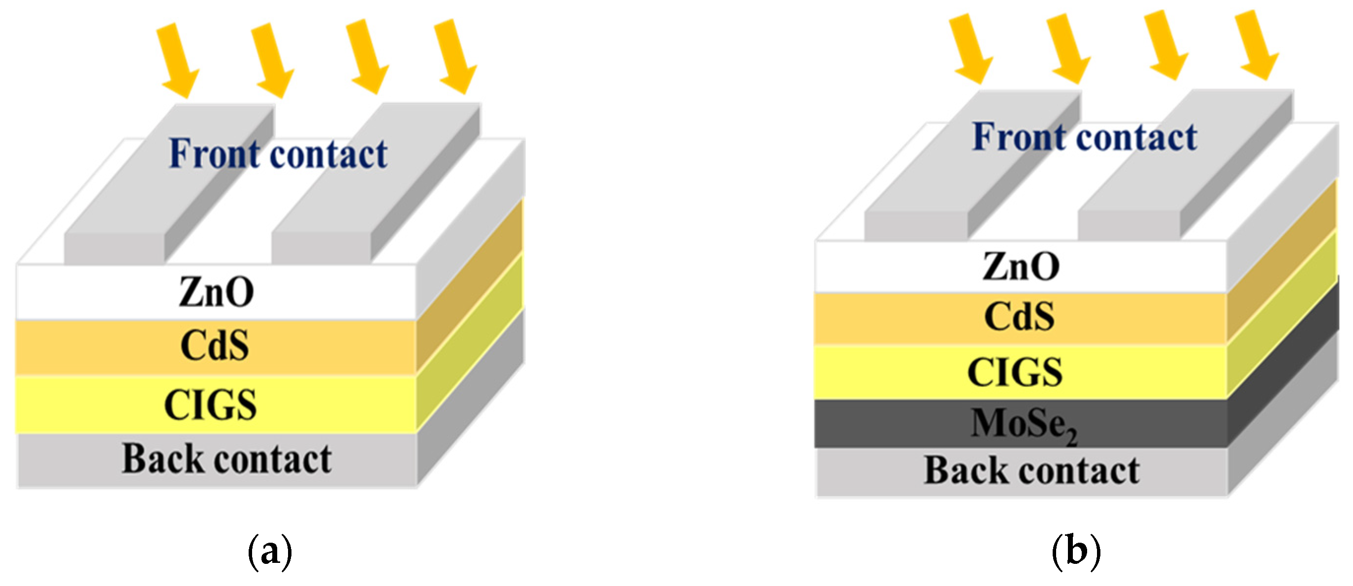
2. Methodology–Device Architecture and Simulation

In this study, we have conducted our investigations extensively using Solar Cell Capacitance Simulator (SCAPS) developed by Prof. Burgelman and his team at the University of Ghent, Belgium. This software solves three numerically basic semiconductor equations: the Poisson equation, the holes continuity equation as well as the electron continuity equation where the steady-state band diagram, recombination profile, and carrier transport in one dimension are calculated [23]. The software will evaluate the solar cell performance mainly through VOC, JSC, FF and PCE.
At the start of the simulations, a reference model based on conventional CIGS solar cell was established. Generally, a conventional CIGS solar cell structure comprises a top electrode, followed by three layers of semiconductor material: zinc oxide (ZnO), which serves as the window layer, cadmium sulfide (CdS) as the n-type buffer layer, and CIGS as the p-type absorber layer. Molybdenum (Mo) is commonly used as the back contact in the device stack as shown in Figure 1a. This architecture is based on the conventional CIGS thin film solar cell structure reported in [24]. In this basic structure, the thickness of the individual layers, the corresponding material properties, as well as the cell’s surface area can all be modified. Since our focus elucidates the influence of the MoSe2 interfacial layer on the PCE of the CIGS device, an additional layer of MoSe2 was inserted into the stack, as presented in Figure 1b. In addition, bandgap gradient was also incorporated into the absorber layer to mirror the bandgap grading in actual devices. Simulation of both the reference and modified devices was performed by setting the optical and electrical parameters for each layer, material Gaussian defect states, and contact parameters as summed up in Table 1, and Table A1 and Table A2 respectively. These parameters are selected on the basis of theoretical considerations, experimental evidence and existing literature [25,26,27]. Table A3 in Appendix A provides an explanation of the symbols used in the previous tables.
In the modified structure shown in Figure 1b, a layer of MoSe2 was inserted in between Mo back contact and CIGS absorber. In order to optimize the proposed solar cell design in this study, properties of MoSe2 layer viz. layer thickness, E g , χ , and N A were varied over the reported values in the range from 0.01 to 0.1 μm, 1.0 to 1.5 eV, 3.5 to 4.5 eV, and 1.0 × 10¹⁴ to 1.0 × 1020 cm−3, respectively. By comparing the performance characteristics (JSC, VOC, FF, PCE) of the proposed layouts against the reference case, the effects due to variations of the MoSe2 layer properties in the cell were investigated. Initially, in order to solely accentuate the effects of the MoSe2 layer properties first, the bandgap of the CIGS absorber was initially kept uniform within the whole absorber layer depth and material parameters for the layers in the solar cell stack other than MoSe2 were also kept unchanged. In the next stage, bandgap grading is introduced into the CIGS absorber layer of the model through the variation of Ga concentration along the layer thickness to ascertain the best grading profile by investigating the influence of the magnitude, shape and depth of the grading. Several grading laws can be implemented in SCAPS: linear, logarithmic, parabolic, power law, exponential, effective medium and a Beta function. These grading laws can be used to set the composition grading over a layer, as well as to set the composition dependence of a property [28]. In this study, parabolic dependence is employed considering that bandgap dependence in most semiconductor alloys A 1 x B x as a function of composition x follows the parabolic function of
( E g ( x ) = ( 1 x ) E g A + x E g B b x ( 1 x )
where E g A and E g B are the band gaps of the pure compounds A and B, respectively, with b as the bowing coefficient [28,29,30]. The following equations are used in this study for extracting the bandgap and electron affinity of CIGS absorber, where x is the Ga percentage or concentration, symbolized in literature as Ga/(In + Ga) (GGI) ratio [26].
E g ( x ) = 1.011 + 0.421 x + 0.244 x 2
χ ( x ) = 4.35 0.421 x 0.244 x 2
According to Equation (2), the bandgap of CIGS surges from 1.011 eV (pure CIS) to 1.676 eV (pure CGS). It should be noted that by implementing a graded composition of the absorber layer, not only the bandgap E g ( x ) , electron affinity χ ( x ) , and optical absorption α ( x , λ ) , other material properties such as dielectric constant, effective density of states, transport properties, defect concentration, recombination properties, etc., also become graded [28]. However, due to the fact that variation of GGI on the other parameters have little effect compared to on E g ( x ) , χ ( x ) , and α ( x , λ ) , other parameters are assumed to be independent of composition in this work. The variation of CIGS optical absorption coefficient α ( x , λ ) caused by change in Ga fraction used in this study is based on work of [31].
As mentioned earlier, alteration of GGI will shift the minimum of the conduction band ( E C ), while the valence band ( E V ) is unaffected by the change. For double grading (DG), E C increases towards both the back contact of CIGS/MoSe2 interface and the front side at the CdS/CIGS junction, as shown in Figure 2 [32,33]. In the case of parabolic law for composition grading, the main parameters are; y l e f t and y r i g h t , indicating the composition at the backside and frontside of the absorber layer, respectively, the notch (the point of minimum Ga composition or lowest bandgap) value and its position across the absorber layer are denoted as y m i n and x m i n [28]. The optimum bandgap grading profile was found by simulating different values for these related bandgap grading parameters as presented in Table 2, and analyzing the corresponding JSC, VOC, FF, and PCE. Previous work by [34] shows that both grading parameters; i.e., the position of the notch and grading height (based on GGI) are equally significant to improve the cell performance through bandgap grading, hence the reason why these parameters were varied in this section. In order to accentuate the effects of bandgap grading, material parameters employed in the simulations were all kept unchanged except for the Ga composition dependent parameters such as bandgap energy, electron affinity, and optical absorption [17]. All simulations were performed under standard test conditions (STC) of AM 1.5 G with an illumination of 1000 W/m2. Finally, a simulation model of CIGS solar cell structure with optimized MoSe2 layer properties and graded absorber is proposed as the main outcome of the work.

3. Results and Discussion

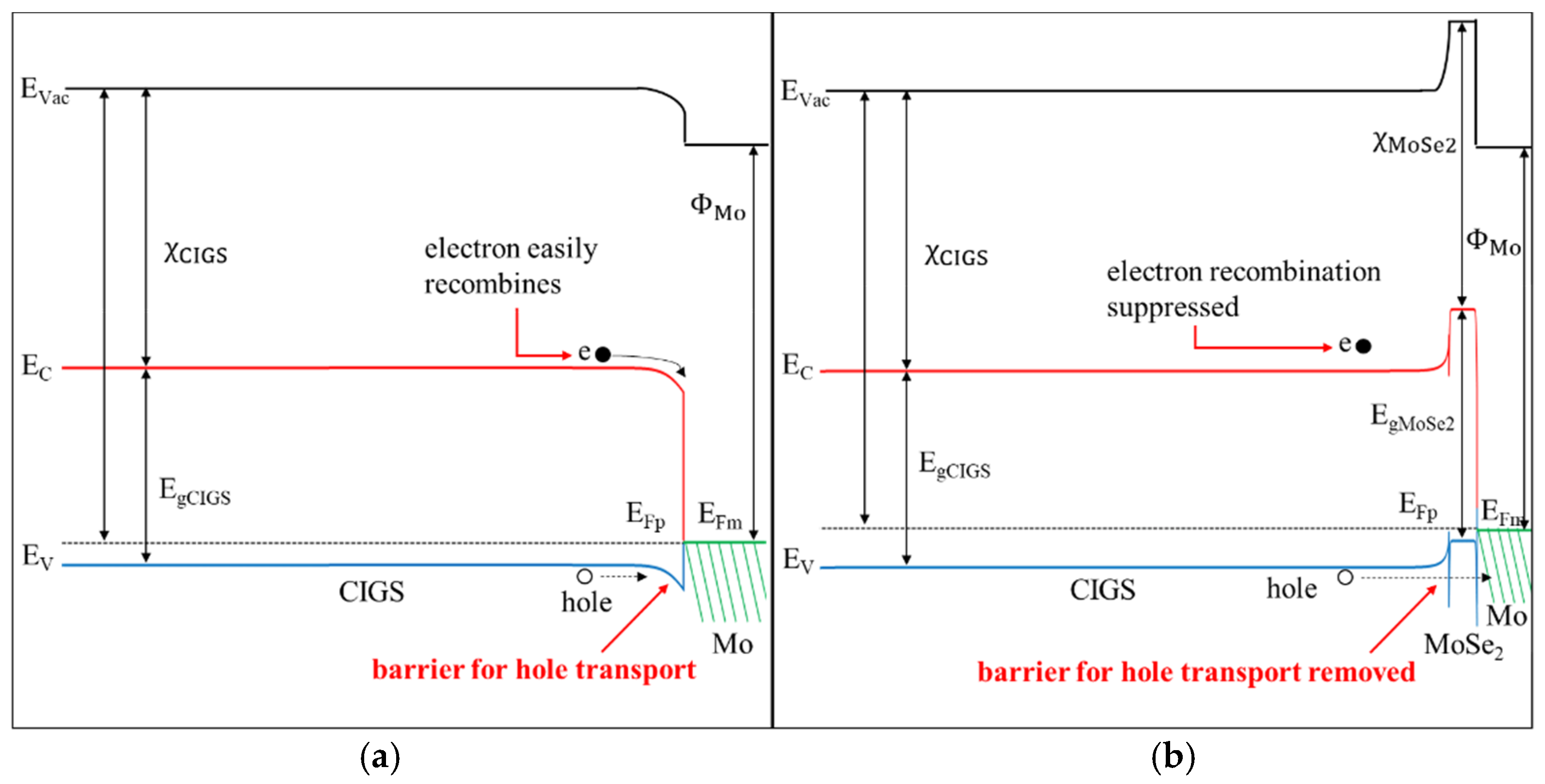
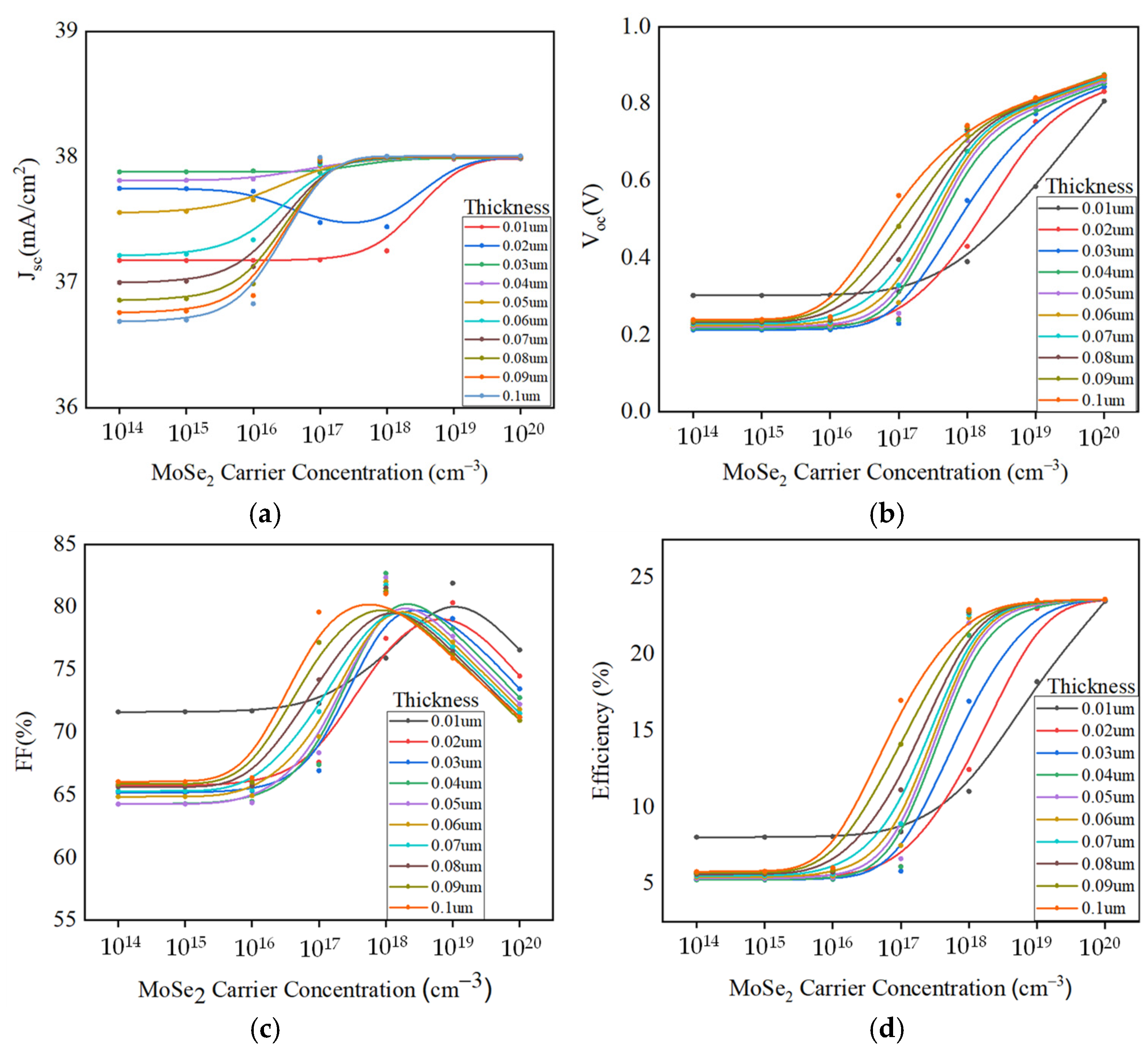
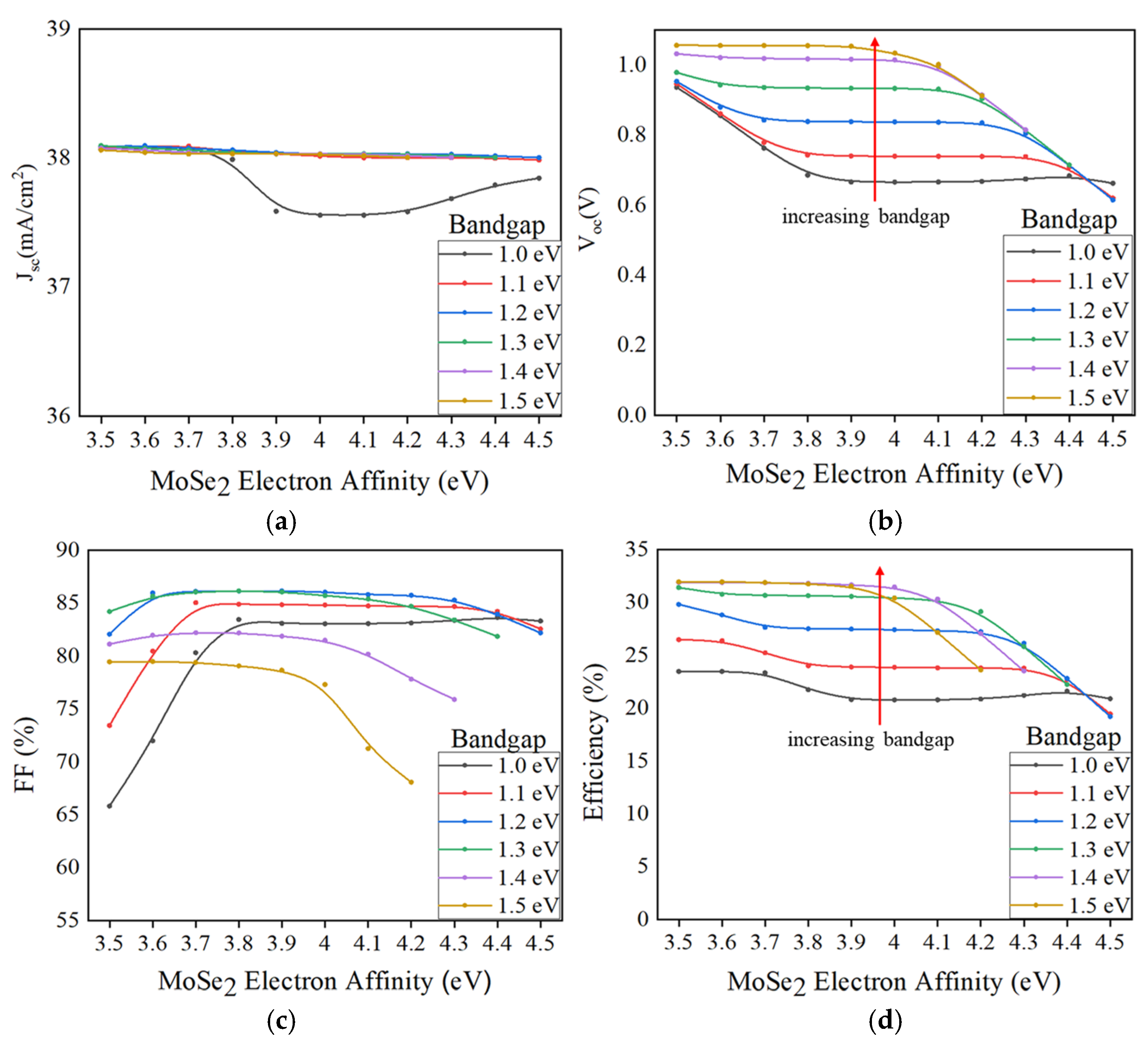
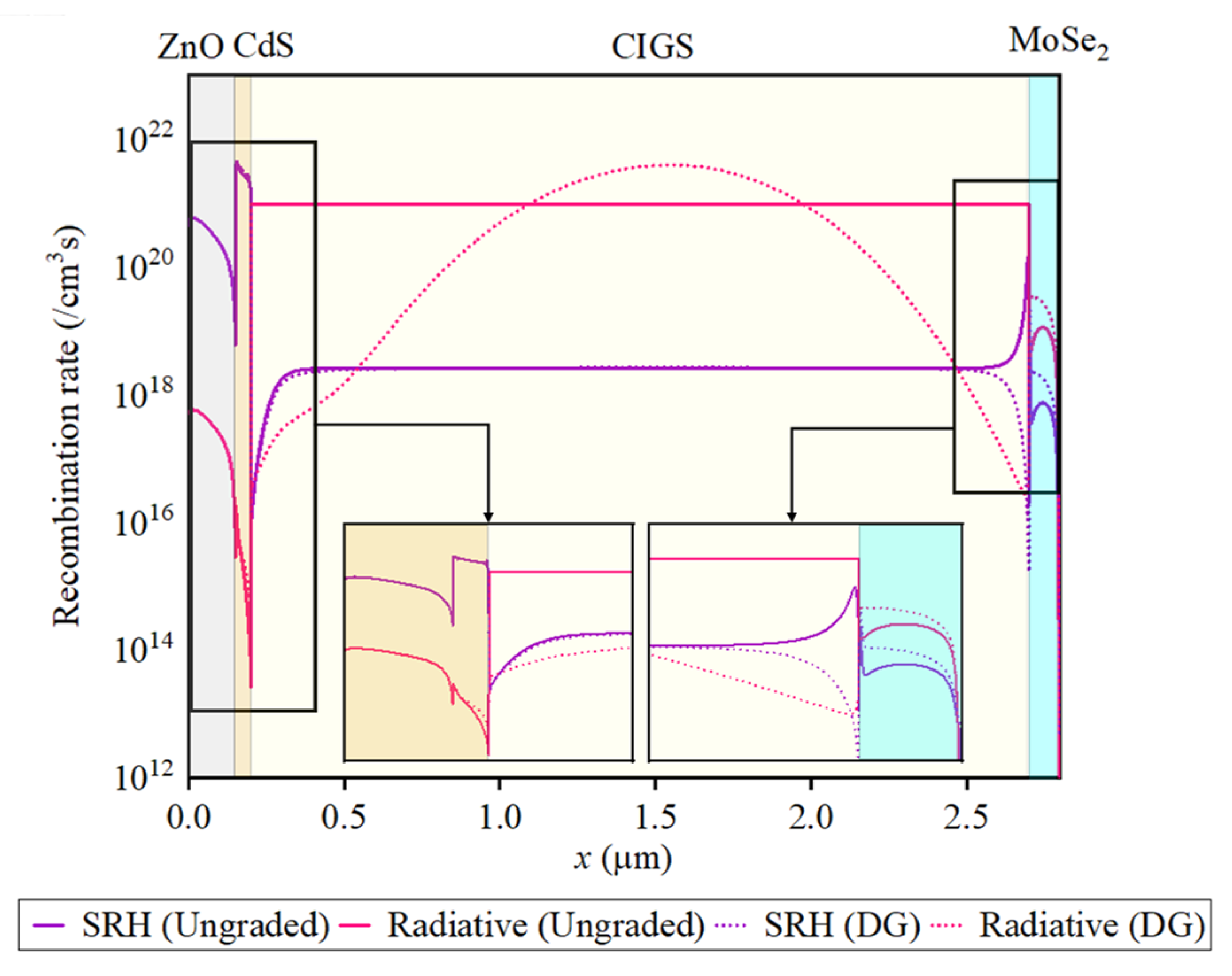
3.1. Study of MoSe2 Interfacial Layer in CIGS Thin Film Solar Cell Structure

It was stated in the Section 2 that ZnO/CdS/CIGS/Mo device structure without any interfacial MoSe2 layer was used as the baseline case in this study. The photovoltaic performance parameters of JSC = 35.75 mA/cm2, VOC = 0.681 V, FF = 82.88%, and PCE = 20.19% for this baseline configuration are considerably lower than all the simulated cases with MoSe2 layer in the structure, which will be shown later. The significantly low cell performance is primarily due to large work function of CIGS, Φ C I G S in comparison to that of Mo, Φ M o ( Φ C I G S > Φ M o ), which results in high barrier for holes ( Φ b p ) at the back contact. This barrier at the back contact interface (CIGS/Mo) is recognized to be an inherent loss mechanism due to the formation of a second junction, but with opposite polarity [35]. It affects other parameters of the solar cell, such as FF and VOC of the device, and hence, the power conversion efficiency (PCE). The emphasis of this part of the numerical analysis is the CIGS/MoSe2/Mo section, which is a semiconductor-semiconductor-metal structure with two interfaces: CIGS/MoSe2 and MoSe2/Mo. Figure 3a shows the band profile of conventional CIGS structure with CIGS/Mo interface in comparison to our proposed structure with CIGS/MoSe2/Mo interface in Figure 3b. The Schottky contact at the CIGS/Mo interface indicated by the large downward bending of the valence band, E V shown in Figure 3a, becomes a quasi-Ohmic contact with the inclusion of a thin MoSe2 semiconducting layer as in Figure 3b. Higher bandgap of MoSe2 leads to upward shift of the conduction band, E C , creating a Δ E C barrier impeding the recombination of minority carriers (electrons) at the back contact that is detrimental to the solar cell performance. In the case of majority carriers (holes) collection, although MoSe2/Mo interface is still a Schottky contact, the formation of the MoSe2 layer shifts both the maxima of the, E V and the minima of the E C upwards, as evident in Figure 3b. This upward shift of the bands results in the elimination of the barrier for holes between the CIGS and Mo layers that is present in Figure 3a. Nevertheless, the collection rate of holes will be suppressed when the MoSe2 interfacial layer is very thick.
In the next stage, optimization of interfacial MoSe2 layer in terms of layer thickness, bandgap energy, electron affinity, and acceptor carrier concentration has been studied to choose the most effective MoSe2 layer properties for the proposed CIGS solar cell design. The effects of acceptor carrier concentration ( N A ) from 1.0 × 10¹⁴ to around 1.0 × 1020 cm−3 and MoSe2 layer thickness from 0.01 to 0.1 μm on the photovoltaic performance of the device were investigated. Figure 4 shows that the overall performance of the device improved when the thickness of MoSe2 layer was increased. This finding arises from the fact that increasing the thickness leads to an increase of photon absorption rate in the near infrared region resulting in higher photogenerated charge carriers, as the MoSe2 layer is effectively extending the width of the p-type region in the solar cell [36]. Additionally, a thinner MoSe2 layer causes lower shunt resistance which is evident from the significantly lower VOC value as can be seen from Figure 4b. This graph depicts the significant dependency of VOC on the two variables of MoSe2; N A and thickness. At N A larger than 1.0 × 1016 cm−3, VOC minutely increased with the increase in thickness until N A   ~ 1.0 × 1018 cm−3, at which point VOC starts to saturate for MoSe2 layer thickness above 0.04 μm, hence the thickness must be maintained above ~ 0.04 μm to obtain the maximum attainable VOC. On the other hand, a thicker MoSe2 layer induces higher series resistance as apparent from the decreased FF in Figure 4c. As such, carrier collection efficiency will be limited due to the increased resistivity of a thick MoSe2 layer in comparison to pure Mo [37]. Therefore, the thickness of MoSe2 layer needs to be carefully controlled to turn the back contact from a rectifying Schottky contact to a low resistance quasi-ohmic contact [38].
On the variations in the MoSe2 carrier concentration, it can be observed that, in general, increasing the N A leads to an increase in the Jsc, Voc, FF as well as the conversion efficiency of the cell, hence higher N A of MoSe2 layer is favorable. MoSe2 layer is found to perform better in terms of JSC and VOC at N A   > 1.0 × 1016 cm−3. This finding can be attributed to the fact that E C and E V rise as N A increases according to [39]. The beneficial band bending facilitates the transport of holes from MoSe2 to Mo, hence enhancing photogenerated carrier collection. At the same time, electrons are hindered from flowing to the back contact thereby inhibiting back surface carrier recombination, enhancing both JSC and VOC. Though the reduced back surface recombination due to band bending with an increase in N A attributes to Voc change, this factor is insufficient to account for observed increase. The significant improvement in VOC for high carrier concentration, N A of MoSe2 can be correlated to the formation of p+-layer at the interface between p-type CIGS and Mo back contact, creating what can be considered as back surface field (BSF) [40]. On the other hand, when the N A of MoSe2 is < 1.0 × 1016 cm−3 which is the value of N A defined for CIGS absorber layer, the overall cell performance degrades. This effect can be described as the phototransistor effect which involves the formation of a second junction, but with opposite polarity to the pn-junction caused by the formation of a Schottky contact in the interfacial region between the MoSe2 with low carrier concentration and the CIGS absorber with higher concentration. As a result, the VOC in the device is impaired [41]. Though phototransistor effect is commonly observed in the J-V curves measured at low temperatures in the range from 100 to 200 K, it was reported that a decrease in the effective doping level of the MoSe2 layer might induce this effect even at room temperature [35,41].
The change in FF with MoSe2 carrier concentration might be discussed and analyzed from the interface properties standpoint. One of the band alignment-related electronic parameter according to Anderson-energy band rule [42] that is significantly affected by the variation in MoSe2 carrier concentration is equilibrium contact potential ( q V o ) that determines potential barrier retarding hole transport from the semiconductor valence band to metal in a Mo/p-type semiconductor structure [43]. Generally, lower q V o is desirable for the hole transport. Increment in the carrier concentration, N A in p-type MoSe2 layer shifts the Fermi level downwards closer to the valence band edge and subsequently increases the semiconductor work function ( Φ M o S e 2 ) and q V o between MoSe2 and Mo as determined by the following equations [42]:
Φ M o S e 2 = χ M o S e 2 + E g M o S e 2 ( k T l n N V N A )
q V o = Φ M o S e 2 Φ M o
Calculated interface electronic parameter values ( Φ M o S e 2 and q V o ) as a function of N A in p-type MoSe2 layer is presented in Table 3 in order to verify the claim. The unfavorable high q V o with the increase in N A forms a larger downward bending barrier for hole transport from the valence band of MoSe2 to the Fermi level of Mo. With barriers larger than 0.2753 eV when N A of MoSe2 was set to 1.0 × 1018 cm−3, the FF starts to degrade.
In terms of different combinations of carrier concentration and thickness, as it is clear in Figure 4a, with high MoSe2 carrier concentration, thin MoSe2 layer is sufficient to achieve high JSC. This is in accordance to the reported findings by Hossain et al. [44] and Ferdaous et al. [45] that even small changes in the JSC values, the phenomenon of higher carrier concentration and lower thickness are preferred for p-type MoS2 (p-MoS2 yields similar benefits as p-MoSe2 as interfacial layer at the back contact). However, Figure 4c shows that when N A is > 1.0 × 1018 cm−3, the trend in FF changes from favoring larger thickness to favoring lesser thickness. Nevertheless, the difference in the electrical characteristics of thin and thick MoSe2 layers are not very significant if the carrier concentration is sufficiently high. Hence, it is more favorable to have a thinner MoSe2 layer with high carrier concentration in order to avoid a jump in series resistance due to the high resistivity nature of MoSe2.
The aforementioned results indicate that significant changes in the performance parameters of the cell were observed when the N A of MoSe2 layer was around 1016, 1018, and 1019 cm−3. Hence, the effects of bandgap energy ( E g ) and electron affinity ( χ ) on the conversion efficiency were investigated in the range from 1.0 to 1.5 eV and 3.5 to 4.5 eV, respectively, at these three domains of N A and are illustrated in Figure 5a,b. As shown, with MoSe2 layer N A of 1018 and 1019 cm−3, CIGS device exhibits similar and almost identical patterns in the PCE with the increase in E g and χ , while at N A of 1016 cm−3, the PCE variation demonstrates a distinguish phenomenon of nearly linear decrease from 20% to 2% and from around 32% to 2% with increasing values of E g and χ , respectively. This result verifies our earlier findings that higher doping level of the MoSe2 layer is more beneficial for the overall cell performance. Therefore, based on this preliminary investigation, N A of MoSe2 layer in the CIGS model was then fixed at 1019 cm−3 to perform further simulations for different combinations of E g and χ for the MoSe2 layer. Figure 6 illustrates the solar photovoltaic parameters as a function of χ of MoSe2 layer, with bandgap energy E g ranging from 1.0 eV to 1.5 eV. It can be observed that, in general, increasing the E g leads to an increase in the conversion efficiency of the cell over the whole investigated range of χ . Hence, MoSe2 layer of higher E g is favorable. As depicted in Figure 6a, for E g   > 1.1 eV, JSC of the device is almost constant for all values of χ , indicating that beyond a minimum value or threshold, E g and χ do not notably affect the current collection. This may be explained by the fact that the thin p-type MoSe2 layer in this CIGS solar cell structure does not play an important role in the photon absorption, hence, other than layer thickness as discussed earlier, variation in other material parameters of this layer does not contribute to the change in JSC of the whole device. On the other hand, VOC and PCE exhibit similar behavior where for the values of E g defined earlier for the MoSe2 layer, the VOC and PCE were almost saturated for all values of χ , provided that E g + χ 5.4 eV. If the total of E g + χ rises beyond 5.4 eV, VOC and PCE start to deteriorate and further increase will result in non-working device as can be seen in Figure 6b,d. These observations indicate that optimum range of electron affinity for a functional MoSe2 interface layer is dependent on the value of its bandgap energy. Improvement in VOC with the increase in E g of MoSe2 layer can be analyzed based on the band offsets at CIGS/MoSe2 and MoSe2/Mo interfaces. The features of band alignment are determined based on the Anderson’s rule or known as electron affinity model as mentioned earlier.
E g and χ of MoSe2 layer crucially determine Φ M o S e 2 , q V o , back contact barrier height with respect to E C ( Φ B n ), back contact barrier height with respect to E V ( Φ B p ) of the MoSe2/Mo metal-semiconductor junction and conduction band offset ( Δ E C ), valence band offset ( Δ E V ), and back diode built-in voltage ( q V b i b a c k ) of the CIGS/MoSe2 heterojunction [46] as given in Equations (4)–(10).
Φ B n = Φ M o χ M o S e 2
Φ B p = E g M o S e 2 Φ B n
Δ E C = χ C I G S χ M o S e 2
Δ E V = ( χ M o S e 2 + E g M o S e 2 ) ( χ C I G S + E g C I G S )  
q V b i b a c k = Φ M o S e 2 Φ C I G S
Increment/decrement in the MoSe2  E g and χ values shifts the whole band structure of the layer upward or downward, which in turn has an effect on the mentioned band alignment related parameters. Nevertheless, since no significant effect on the cell performance is found in the variation of χ in comparison to E g from our earlier discussion on Figure 6, χ is defined as 3.9 eV in order to calculate the interface electronic parameter values as a function of E g as tabulated in Table 4. Changes in E g are usually reflected as simultaneous change in E C and E V . Thus, any increase in E g can be seen as upshifting of E C and/or downshifting of E V . However, since the value of χ was kept constant, the increase in E g is assumed to cause the downshifting of E V , while E C does not change, thus the values of Φ B n and Δ E C are constant with the increase in E g , as shown in Table 4. Therefore, the resulting device performance is solely a composite function of Φ B p , q V o , Δ E V and q V b i b a c k . In general, for CIGS/MoSe2/Mo band alignment, lower q V o and Δ E V along with higher positive q V b i b a c k (or lower negative q V b i b a c k ) are desirable for greater hole transport across the valence band of CIGS to valence band of MoSe2 and from the valence band of MoSe2 to Mo metal. Increase of MoSe2 E g results in an increase in MoSe2 work function ( Φ M o S e 2 ) due to the downward shift of E V . This will lead to larger values of Φ B p , q V o and Δ E V , compounding the inhibition of hole flow to the back contact. Nevertheless, this drawback can be negated by carrier tunneling through a very thin MoSe2 layer, which can be related back to the improved conversion efficiency obtained with the increase in E g as illustrated in preceding Figure 6d. Additionally, increased hole population by means of higher doping concentration can yield slightly better performance for MoSe2 with higher E g as previously demonstrated in Figure 5.
Based on the aforesaid results, variations in the bandgap, electron affinity, thickness and carrier concentration of the MoSe2 layer mainly affected the band alignment at the CIGS/MoSe2 and MoSe2/Mo junctions, which subsequently influences the overall performance of the CIGS solar cell. It was identified that a MoSe2 layer with bandgap in the range of 1.2 eV to 1.4 eV and high carrier concentration above 1.0 × 1018 cm−3 is beneficial for the PV cell. As predicted, the MoSe2 layer needs to be quite thin, but not less than 0.04 μm thickness in order to be effective or operational. These findings provide a limiting condition for MoSe2 layer in CIGS solar cell since the formation is absolutely unavoidable during the growth process. Our CIGS model with optimized MoSe2 layer is then validated by comparison with extant experimental results for the conventional ZnO/CdS/CIGS/Mo solar cells considering that MoSe2 is naturally formed as opposed to being a deliberately added layer in the device stack during fabrication. The 23.3% efficiency of our simulated CIGS cell is significantly higher with the addition of MoSe2 layer than the recorded efficiency of 21.7% [24]. This is apparently due to the fact that there are many other factors during the fabrication process that could affect the cell performance that cannot be replicated by the simulation software. Therefore, it is impossible to simulate these realistic experimental conditions due to the limitations of the SCAPS software. In addition, not many details were provided in the report about the actual steps involved in the making of these record-breaking solar cells. Nevertheless, the adequately high efficiency of the actual solar cells suggests the presence of MoSe2 layer in the structure as the simulated structure with MoSe2 is closer to the experimental value. The resulting performance parameters of the JSC, VOC, FF and PCE are displayed in Table 5.

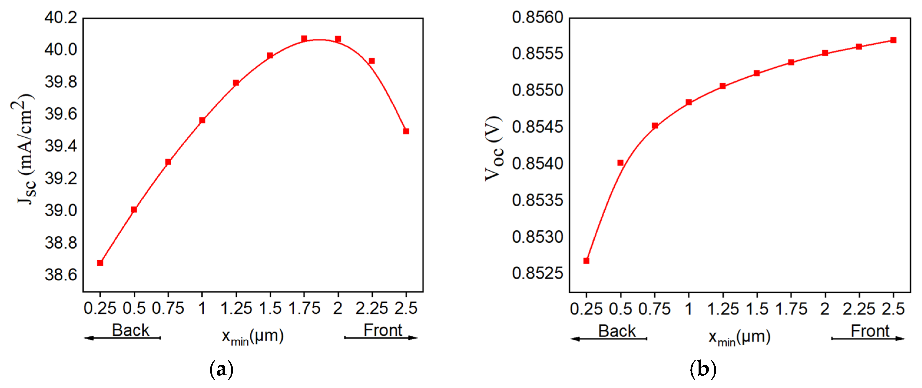
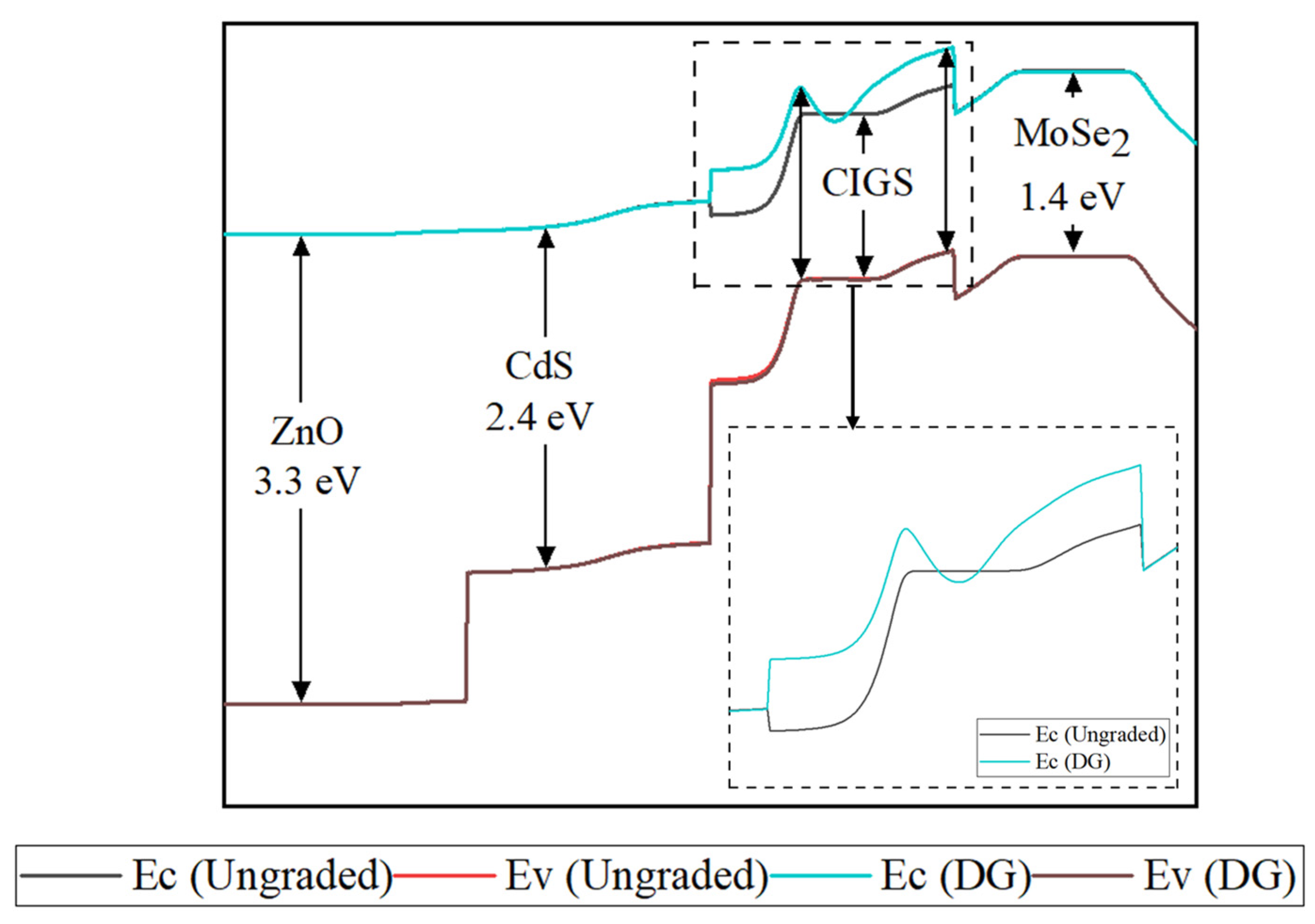
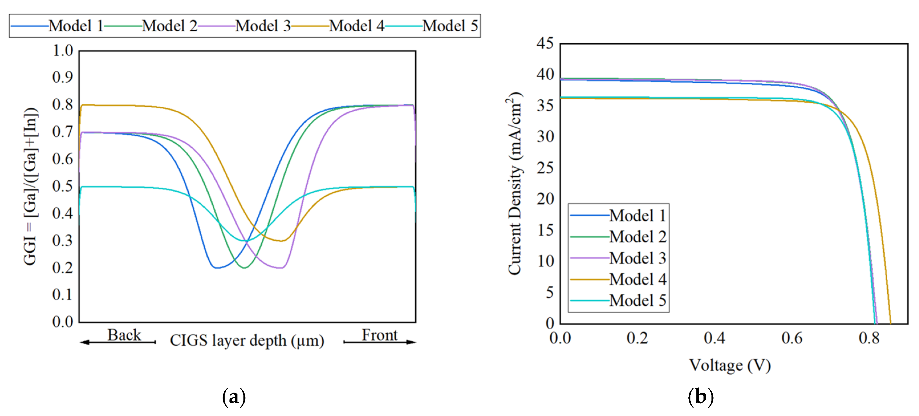
3.2. Study of Absorber Layer Bandgap Grading in CIGS Solar Cell Structure

In this study, bandgap grading was introduced into the model by including a Ga concentration profile in the absorber layer, that is the variation of GGI ratio throughout the depth of the absorber layer. Double grading (DG) profile was defined within the absorber layer, which corresponds to a minimum amount of Ga in the middle layer region and a higher amount toward the CIGS/MoSe2 and the CdS/CIGS interfaces. These bandgap variations are described in this work by the parameters: (i) y l e f t and y r i g h t (corresponding to the Ga concentration at the back and front sides of the absorber layer); (ii) y m i n (notch point which represents the lowest composition value); (iii) x m i n (position of the notch point across the depth of absorber layer) through the use of parabolic grading [28]. Thus, y l e f t and y r i g h t define the E g , m a x (maximum bandgap value) while y m i n defines E g , m i n (minimum bandgap value) in the bandgap grading profiles. With the purpose of determining the best grading configuration for this notch type double graded bandgap structure in our CIGS model, different values for these related bandgap grading parameters were simulated and the effects on cell performance were analyzed. In order to incorporate an optimum DG bandgap profile, the effects of separate grading at either ends of the absorber must be first understood. Thereby, optimization of single graded Ga profiles (back and front grading) was conducted prior to the introduction of DG and the results obtained are illustrated in Figures S2–S4 in the supporting materials section. Table 6 shows the optimum values for Ga composition (GGI ratio) at the back contact and at the CdS/CIGS interface and the lowest bandgap ( y m i n ) in the CIGS absorber layer obtained from the optimization of single graded Ga profiles.
Conceptually, double graded (DG) bandgap absorbers promote photovoltaic performance by increasing JSC, which is a consequence of the minimum bandgap introduced in the absorber layer of the device, and at the same time increased VOC due to the increased bandgap in the SCR. This principal of two bandgaps was experimentally verified by Dullweber et al. [47]. In DG bandgap profile, the position of notch ( x m i n ) is a significant parameter that will influence the effectiveness of bandgap grading in the absorber layer. Hence, x m i n is varied in the range from 0 to 2.5 μ m to observe the effects mainly on JSC and VOC, keeping the notch value ( y m i n ) constant at 0.3. From Figure 7a, it can be observed that JSC significantly improved when the x m i n value is shifted to the front junction of the CIGS layer. As mentioned earlier in Section 1, absorption in the frontal part is reduced as the bandgap in this region becomes larger. However, if the front grading with wider bandgap is restricted within the SCR by placing the notch ( x m i n ) inside the width of SCR, the loss in JSC can be compensated by an increased absorption further into the CIGS absorber layer, where the band gap is minimum. Moreover, the rise of E g in the SCR will generate an additional electric field that will oppose the transport of electrons. Hence, it is important to confine the front grading only in this region. As x m i n shifts further towards the backside of the absorber layer (from the distance of 2.25 to 0.25 μ m), the decrease in JSC is more pronounced (from 38.97 to 36.37 mA/cm2). The graph in Figure 7b depicts VOC dependency on the notch position ( x m i n ) that is fairly contrasting to JSC. VOC does not seem to be substantially affected by the variation in x m i n , though small increment is observed as x m i n shifts towards the front side of the absorber layer.
There are certain conditions related to the grading parameters that must be satisfied in order to completely benefit from bandgap grading. In the case of a p-type CIGS layer, the needed quasi-electric field arising from an absorber material with graded bandgap structure should be directed towards the back contact so that electrons will drift in the opposite direction to reduce back surface recombination. In other words, in this case, the bandgap must be larger towards the back contact. The second condition is that the formation of wider bandgap region at the front junction must be confined within SCR since this quasi-electric field would oppose the motion of photo-generated carriers from the bulk of the semiconductor towards the collecting junction. From the above considerations, different magnitudes, shapes, and depths of double graded (DG) bandgap structure were tested in order to find its relevance in the solar cell performance and to determine the best grading configuration for an optimized CIGS device. Figure 8a illustrates the simulated compositional ratios of five models with different bandgap configurations and the resulting current density-voltage (J-V) curves obtained are shown in Figure 8b. A summary of the solar cell parameters for the different Ga profiles is presented in Table 7.
As can be observed in Table 7, the best PCE is obtained from the simulated Model 2 that presents a front grading and back grading composition of 0.8 and 0.7, respectively. The notch for this model is positioned at a distance of 1.25 μm from the CdS/CIGS interface. Although it is mentioned earlier that the notch should be placed close to the junction and restricted within the SCR for improved JSC as evident from previous Figure 7a, 1.25 μm was found to be the optimum notch position for the DG absorber bandgap profile developed in this study. The slight loss in JSC in Model 3 in comparison to Model 2, with Model 3 having a steeper Ga grading profile at the frontside of the absorber, can be attributed to the fact that the notch acts like a confinement region for electrons decreasing photogenerated carrier collection probability. Similar observation can be made for Model 4 and Model 5. In line with the reflection that improved JSC in DG absorber bandgap structure is controlled by the minimum bandgap value in the layer, it can be discerned that JSC values are higher when y m i n was set at GGI = 0.2 as compared to 0.3 in all bandgap grading models. With regard to VOC, Model 4 presents the highest value of 0.856 V that can be attributed to the highest GGI ratio of 0.8 ( E g , b a c k = 1.5 eV) at the backside of the absorber layer. The enhanced VOC is directly correlated to the reduced back surface recombination as discussed and presented in the earlier section. FF is the highest in device Model 5 with DG absorber bandgap value of 1.28 eV corresponding to GGI (=0.5) at both the frontside and backside of the absorber layer. Ideally, FF is only a function of VOC. However, practically, FF does not only depend on VOC, but also on the recombination process in the depletion region [45], which explains the difference in the trend of FF in comparison to VOC as can be seen in Table 7. The highest PCE gain from the ungraded bandgap cell is over 8.8% as seen in Model 2.

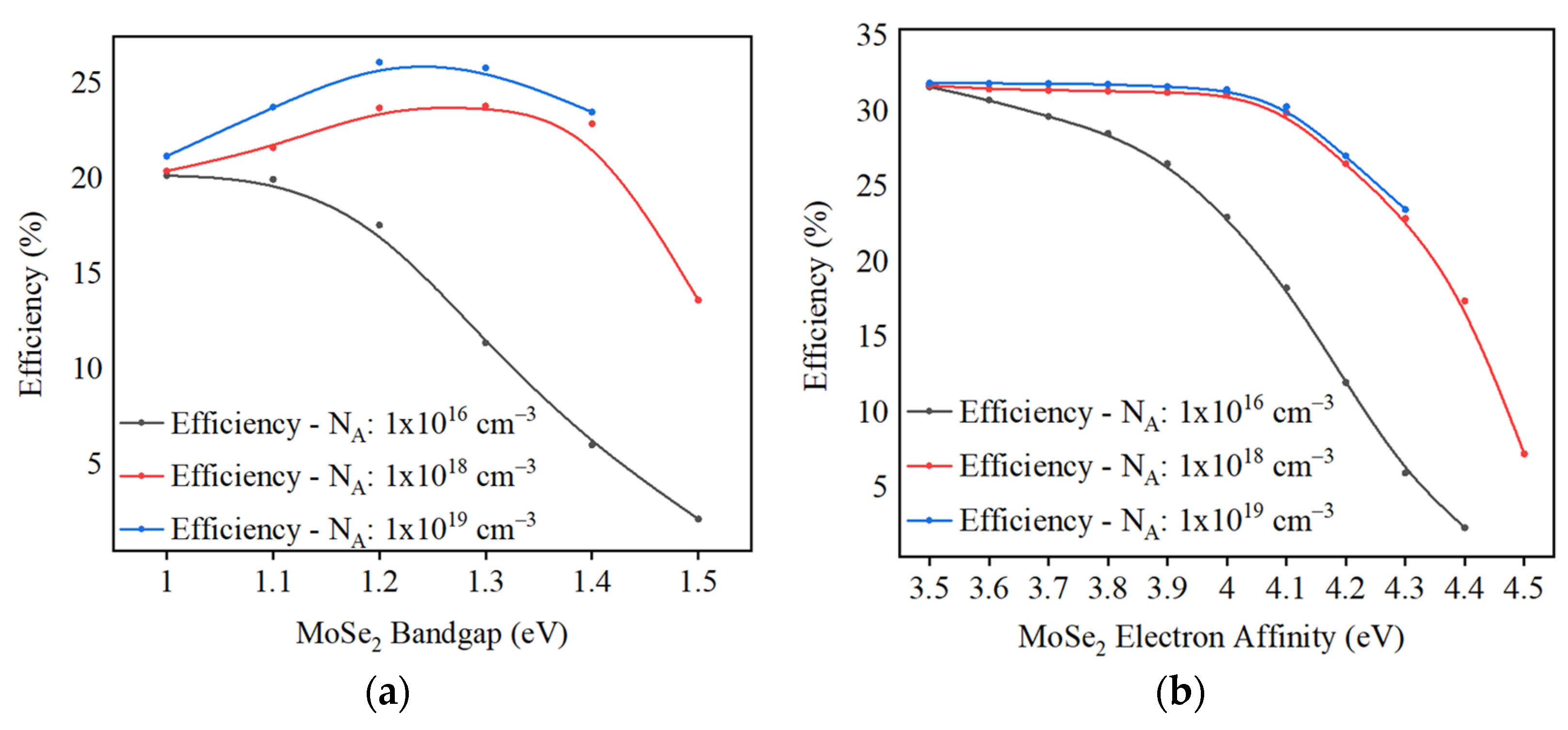
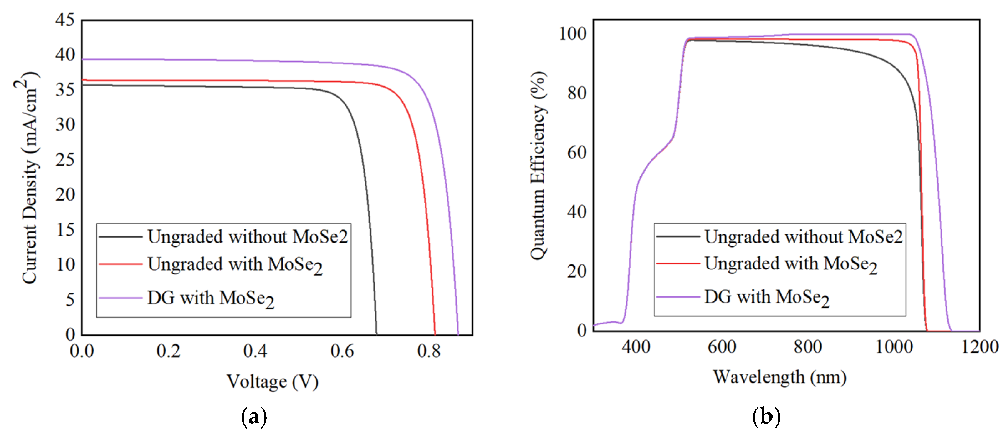
3.3. Optimizing Bandgap Energy of MoSe2 Layer for Compatibility with Double Graded (DG) Bandgap Profile of CIGS Absorber Layer

For the purpose of associating the bandgap grading study with MoSe2 layer properties, optimum DG bandgap profile with front and back GGI ratio of 0.8 and 0.7, respectively, x m i n = 1.25 μm, and y m i n = 0.2 as previously determined was employed with MoSe2 layers with varying bandgaps of 1.0 to 1.4 eV. The resulting solar photovoltaic parameters (JSC, VOC, FF and PCE) obtained are tabulated in Table 8. In Section 3.1, it has been shown that E g and χ of both MoSe2 and CIGS layers are vital in determining the Δ E C , Δ E V , and q V b i b a c k of the CIGS/MoSe2 heterojunction [43]. Lower Δ E V and higher positive q V b i b a c k (or lower negative q V b i b a c k ) are desirable for the ease of hole transport across the valence band of the CIGS layer to the valence band of MoSe2. Hence, the resulting device performance is partly contributed by the composite function of Δ E V and q V b i b a c k . The effects of MoSe2 bandgap on these parameters have been discussed and presented in Section 3.1. Based on the values of JSC, VOC, FF and PCE in Table 8, MoSe2 bandgap of 1.3 eV is the best match with E g , b a c k of 1.43 eV at the backside of CIGS absorber layer for devices with DG absorber bandgap profile.
It is a fact that recombination of photo-generated carriers is the main detrimental factor affecting the performance of CIGS solar cells [46,47,48]. Extraction of interface recombination rates allows detailed analysis for material and device engineering to reduce interface recombination leading to an improved VOC. Though experimental VOC analysis is compulsory in understanding the physics of recombination mechanism, previous investigation has demonstrated the possibility of utilizing numerical simulation for extracting recombination rates in the complete width of the absorber layer (from the buffer/absorber interface [48] to absorber/back contact interface [49]). The principle of temperature- and illumination-dependent VOC analysis is to identify and quantify Shockley–Read–Hall (SRH) as well as radiative recombination rates in different regions of the CIGS absorber-namely, the heterointerface, depletion region and quasi-neutral region (QNR). A study conducted by Paul et al. [50] depicted that most of the recombination occurs near the CdS buffer/CIGS absorber interface and in the depletion region, with Shockley–Read–Hall (SRH) recombination dominating over radiative recombination when operating temperature, T is set at 300 K. By emulating the investigation carried out by Paul et al., simulation study on the relationship of recombination rate and the depth of the absorber layer was carried out using the baseline CIGS model at V = VOC. The MoSe2 interface layer and absorber bandgap grading was not incorporated in this baseline CIGS model. Uniform mid-gap defect level for all layers in the structure were considered, with radiative recombination coefficient defined as 1.0 × 10⁻¹⁰ cm3/s based on [50]. Figure 9 shows the generated SRH and radiative recombination profiles (for T = 300 K) at V = VOC. It was found that the interface of CdS/CIGS and SCR act as recombination centers in the structure, matching the observations made by [50]. However, in this study radiative recombination rate seems to be higher at the depletion region and QNR while SRH is significantly more dominant at the front interface. There was not much difference in the recombination rates with the variation in operating temperature, T = 200 K and 300 K.
Controlling bandgap grading within the CIGS absorber is claimed to be one way of improving band alignment and suppressing recombination at the interface and in the bulk of the layer. It is said that in a uniform bandgap absorber with a low Ga content, recombination in the quasi-neutral region dominates, while in the high Ga-absorber, interface recombination dominates [51]. However, the effect of bandgap grading on the recombination process has not yet been fully understood. Hence, one of the objectives for implementing a graded structure in this study is to rearrange the recombination throughout the cell, by optimizing CdS/CIGS and CIGS/MoSe2 band offsets to reduce surface recombination at the interface and by utilizing the built-in potential that causes drift of the photogenerated electrons and holes towards the right direction. In order to understand the role that bandgap grading has in suppressing carrier recombination, recombination profiles for the simulated CIGS device with MoSe2 interfacial layer and with/without graded structure (DG) in the absorber layer were analyzed and presented in Figure 10 (left inset). There was clear benefit to be seen in recombination yields with the introduction of bandgap grading as suggested by earlier studies, with a significant decrease in back surface and front surface recombination illustrated in Figure 10 left and right inset respectively. Additional electric field known as quasi-electric field ( ξ A ) is formed due to the change in bandgap, E g over the distance x and can be described by Equation (11) [20]. This quasi-electric field directed towards the back contact with the introduction of back grading will drift the electrons in the opposite direction to reduce back surface recombination. Hence. Ga-rich structure at the backside of absorber layer (towards CIGS/MoSe2 interface) is beneficial and effective in suppressing electrons from combining with holes.
ξ A = d Δ E g d x
With respect to the front surface recombination, recombination rate in the SCR can be reduced by increasing the barrier height via the increase of bandgap at the junction region (CdS/CIGS interface). This is due to the fact that the CdS buffer/CIGS absorber conduction-band offset, Δ E C significantly influences the band bending and thereby affecting interface recombination where stronger band bending and larger hole barrier are induced by a positive Δ E C at the CdS/CIGS interface [49].
By comparing the J-V characteristic and quantum efficiency (QE) curves of a uniform bandgap device with and without MoSe2 layer to the device with DG absorber profile, shown in Figure 11, the composite benefit of the MoSe2 layer and DG absorber layer on the performance of CIGS solar cells, is remarkable and was clearly demonstrated in this simulation study, as seen in the overall cell performance parameters. This enhancement in current density is attributed to the increased absorption of photons in the longer wavelength region of above 1000 nm, as can be seen from the QE curve of Figure 11b. A reasonable explanation for the enhanced photon absorption is the lower E g , m i n of 1.10 eV in the underlying bulk region of DG CIGS absorber layer in comparison to the device with uniform absorber bandgap of 1.20 eV. This observation is in agreement with the inferred statement earlier that this notch value and its position is crucial for the device to benefit from bandgap grading of the absorber layer. Table 9 below shows the performance parameters of all the devices investigated in this section.

4. Conclusions

Via the use of SCAPS software, a comprehensive numerical simulation analysis of CIGS thin film solar cell having additional MoSe2 interface layer with varying material properties and various absorber bandgap profiles has been performed. The primary objective of this work was to investigate the simultaneous effects of MoSe2 layer and Ga grading of the absorber in suppressing carrier losses due to back contact recombination and resistance that usually happen in the case of standard Mo thin films. Numerical simulations were performed to analyze the dependence of output parameters such as JSC, VOC, FF and PCE to a wide range of thickness, carrier concentration, E g and χ of MoSe2 layer as well as to different kinds of related grading parameters that can be optimized through the incorporation of bandgap grading in the absorber layer. From the obtained results, it was identified that MoSe2 with E g of 1.3 eV and high carrier concentration above 1.0 × 1019 cm−3 can be beneficial for the CIGS solar cell. It was also shown that the MoSe2 layer needs to be very thin in the range of 0.04 to 0.1 μm in order to be effective. With regard to bandgap grading, it is evident from our results that an in-depth control of back and front Ga composition and the position of notch that correlates to the lowest bandgap value in the absorber layer is necessary to produce high performing solar cell. With the incorporation of double grading (DG) bandgap profile in the absorber layer, the performance of our simulated CIGS cell was significantly enhanced, achieving the highest efficiency of 28.06%. In summary, CIGS thin film solar cells with a functional MoSe2 contact layer and a suitable double graded bandgap absorber layer are key focus areas in achieving higher photovoltaic conversion efficiencies.

Supplementary Materials

The following are available online at https://www.mdpi.com/article/10.3390/coatings11080930/s1, Figure S1: Measured J–V curves with different illumination values. Plots (ac) correspond to the simulated CIGS device with carrier concentration of MoSe2 interfacial layer of 1.0 × 10¹⁴, 1.0 × 10¹⁶, and 1.0 × 1019 cm−3, respectively, at T = 300 K. Figure S2: Electrical parameters as a function of back (CIGS/MoSe2 interface) composition ranging from 0 to 1 for BG structure (a) JSC and VOC (b) FF and conversion efficiency (PCE). Figure S3: Electrical parameters as a function of front (CdS/CIGS interface) composition ranging from 0 to 1 for FG structure (a) JSC and VOC (b) FF and conversion efficiency (PCE). Figure S4: Electrical parameters as a function of as a function of lowest composition value ( y min ) in the bulk region of CIGS absorber layer for FG bandgap profile (a) JSC and VOC (b) FF and conversion efficiency (PCE).

Author Contributions

Conceptualization, Y.Y., F.I.Z. and P.C.; methodology Y.Y. and F.I.Z.; validation, P.C., N.A., K.S.R. and N.A.S.; formal analysis, Y.Y. and F.I.Z.; investigation, F.I.Z., M.S.B. and W.S.W.A.; writing—original draft preparation, F.I.Z.; writing—review and editing, Y.Y. and P.C.; supervision, N.A., S.F.A. and A.W.M.Z.; funding acquisition, A.W.M.Z. and H.M. All authors have read and agreed to the published version of the manuscript.

Funding

This research project was funded by Universiti Tenaga Nasional through its UNITEN BOLD 2021 grant (J510050002/2021082).

Institutional Review Board Statement

Not applicable.

Informed Consent Statement

Not applicable.

Data Availability Statement

Data is contained within the article or supplementary material.

Acknowledgments

The authors would like to acknowledge Burgelman’s group from University of Ghent, Belgium for providing the SCAPS simulator that is available at the SCAPS website https://scaps.elis.ugent.be/ (accessed on 15 January 2021). The publication of this work was supported by UNITEN BOLD Publication Fund.

Conflicts of Interest

The authors declare no conflict of interest exists with any parties. The funders had no role in the design of the study; in the collection, analyses, or interpretation of data; in the writing of the manuscript or in the decision to publish the results.

Appendix A

Table A1. Simulation Material Gaussian Defect for the CIGS Solar Cell.
MaterialZnOCdSCIGSMoSe2
Defect typeDonorDonorAcceptorAcceptor
Energy level (eV)1.651.20.60.7
σ n (cm2)1.0 × 10−151.0 × 10−175.3 × 10−135.3 × 10⁻¹³
σ p (cm2)1.0 × 10−129.8 × 10−131.0 × 10−181.0 × 10⁻¹⁸
N t (cm−3)1.0 × 10161.0 × 10181.0 × 10141.0 × 1014
Table A2. Contact Parameters Applied in the Simulation.
ParameterBack ContactFront Contact
ϕ B (eV)0.6348Flat band
S n (cm/s)1.0 × 1071.0 × 107
S p (cm/s)1.0 × 1071.0 × 107
ReflectivityNA0.02
Table A3. Definition of the Parameters Used During the Simulations.
ParameterDefinition
ε r Dielectric permittivity
μ n / μ p Mobility of electron/holes
N A / N D Acceptor/donor concentration
E g Bandgap energy
N C / N V Effective density of states in the conduction/valence band
χ Electron affinity
σ n / σ p Capture cross section of electron/holes
N t Defect concentration
ϕ B Barrier height
S n / S p Surface recombination velocity of electron/holes

References

  1. Green, M.A.; Dunlop, E.D.; Hohl-Ebinger, J.; Yoshita, M.; Kopidakis, N.; Ho-Baillie, A.W.Y. Solar cell efficiency tables (Version 55). Prog. Photovolt. Res. Appl. 2020, 28, 3–15. [Google Scholar] [CrossRef]
  2. Siebentritt, S. What limits the efficiency of chalcopyrite solar cells? Sol. Energy Mater. Sol. Cells 2011, 95, 1471–1476. [Google Scholar] [CrossRef]
  3. Kohara, N.; Nishiwaki, S.; Hashimoto, Y.; Negami, T.; Wada, T. Electrical properties of the Cu(In,Ga)Se2/ MoSe2/Mo structure. Sol. Energy Mater. Sol. Cells 2001, 67, 209–215. [Google Scholar] [CrossRef]
  4. Nishiwaki, S.; Kohara, N.; Negami, T.; Nishitani, M.; Wada, T. Characterization of Cu(In,Ga)Se2/Mo Interface in CIGS Solar Cells. MRS Proc. 1997, 485, 139. [Google Scholar] [CrossRef]
  5. Klinkert, T.; Theys, B.; Patriarche, G.; Jubault, M.; Donsanti, F.; Guillemoles, J.F.; Lincot, D. New insights into the Mo/Cu(In,Ga)Se2 interface in thin film solar cells: Formation and properties of the MoSe2 interfacial layer. J. Chem. Phys. 2016, 145, 154702. [Google Scholar] [CrossRef]
  6. Wada, T.; Kohara, N.; Nishiwaki, S.; Negami, T. Characterization of the Cu(In,Ga)Se2/Mo interface in CIGS solar cells. Thin Solid Films 2001, 387, 118–122. [Google Scholar] [CrossRef]
  7. Neugebohrn, N.; Hammer, M.S.; Neerken, J.; Parisi, J.; Riedel, I. Analysis of the back contact properties of Cu(In,Ga)Se2solar cells employing the thermionic emission model. Thin Solid Films 2015, 582, 332–335. [Google Scholar] [CrossRef]
  8. Wei, S.-H.; Zunger, A. Effects of Ga addition to CuInSe2 on its electronic, structural, and defect properties. Appl. Phys. Lett. 1998, 72, 3199–3201. [Google Scholar] [CrossRef] [Green Version]
  9. Cai, C.-H.; Chen, R.-Z.; Chan, T.-S.; Lu, Y.-R.; Huang, W.-C.; Yen, C.-C.; Zhao, K.; Lo, Y.-C.; Lai, C.-H. Interplay between potassium doping and bandgap profiling in selenized Cu(In,Ga)Se 2 solar cells: A functional CuGa: KF surface precursor layer. Nano Energy 2018, 47, 393–400. [Google Scholar] [CrossRef]
  10. Morales-Acevedo, A. A simple model of graded band-gap CuInGaSe2 solar cells. Energy Procedia 2010, 2, 169–176. [Google Scholar] [CrossRef] [Green Version]
  11. Gloeckler, M.; Sites, J.R. Band-gap grading in Cu(In,Ga)Se2solar cells. J. Phys. Chem. Solids 2005, 66, 1891–1894. [Google Scholar] [CrossRef]
  12. Saadat, M.; Moradi, M.; Zahedifar, M. CIGS absorber layer with double grading Ga profile for highly efficient solar cells. Superlattices Microstruct. 2016, 92, 303–307. [Google Scholar] [CrossRef]
  13. Zheng, X.; Li, W.; Aberle, A.G.; Venkataraj, S. Efficiency enhancement of ultra-thin Cu(In,Ga)Se 2 solar cells: Optimizing the absorber bandgap profile by numerical device simulations. Curr. Appl. Phys. 2016, 16, 1334–1341. [Google Scholar] [CrossRef]
  14. Aissani, H.; Helmaoui, A.; Moughli, H. Numerical Modeling of Graded Band-Gap CIGS Solar Celle for High Efficiency. Int. J. Appl. Eng. Res. 2017, 12, 227–232. [Google Scholar]
  15. Song, J.; Li, S.S.; Huang, C.H.; Crisalle, O.D.; Anderson, T.J. Device modeling and simulation of the performance of Cu(In1-x,Gax)Se2solar cells. Solid State Electron. 2004, 48, 73–79. [Google Scholar] [CrossRef]
  16. Huang, C.H. Effects of Ga content on Cu(In,Ga)Se2 solar cells studied by numerical modeling. J. Phys. Chem. Solids 2008, 69, 330–334. [Google Scholar] [CrossRef]
  17. Amin, N.; Chelvanathan, P.; Hossain, M.I.; Sopian, K. Numerical modelling of ultra thin Cu(In,Ga)Se2solar cells. Energy Procedia 2012, 15, 291–298. [Google Scholar] [CrossRef] [Green Version]
  18. Kuo, S.-Y.; Hsieh, M.-Y.; Hsieh, D.-H.; Kuo, H.-C.; Chen, C.-H.; Lai, F.-I. Device Modeling of the Performance of Cu(In,Ga)Se2 Solar Cells with V-Shaped Bandgap Profiles. Int. J. Photoenergy 2014, 2014, 186579. [Google Scholar] [CrossRef]
  19. Lundberg, O.; Edoff, M.; Stolt, L. The effect of Ga-grading in CIGS thin film solar cells. Thin Solid Films 2005, 480, 520–525. [Google Scholar] [CrossRef]
  20. Park, J.; Shin, M. Numerical Optimization of Gradient Bandgap Structure for CIGS Solar Cell with ZnS Buffer Layer Using Technology Computer-Aided Design Simulation. Energies 2018, 11, 1785. [Google Scholar] [CrossRef] [Green Version]
  21. Belghachi, A.; Limam, N. Effect of the absorber layer band-gap on CIGS solar cell. Chin. J. Phys. 2017, 55, 1127–1134. [Google Scholar] [CrossRef]
  22. Khoshsirat, N.; Md Yunus, N.A.; Hamidon, M.N.; Shafie, S.; Amin, N. Analysis of absorber layer properties effect on CIGS solar cell performance using SCAPS. Optik 2015, 126, 681–686. [Google Scholar] [CrossRef]
  23. Burgelman, M.; Verschraegen, J.; Minnaert, B.; Marlein, J. Numerical simulation of thin film solar cells: Practical exercises with SCAPS. In Proceedings of the International Workshop on Numerical Modelling of Thin Film Solar Cells (NUMOS), Gent, Belgium, 28–30 March 2007. [Google Scholar]
  24. Jackson, P.; Hariskos, D.; Wuerz, R.; Kiowski, O.; Bauer, A.; Friedlmeier, T.M.; Powalla, M. Properties of Cu(In,Ga)Se2solar cells with new record efficiencies up to 21.7%. Phys. Status Solidi-Rapid Res. Lett. 2015, 9, 28–31. [Google Scholar] [CrossRef]
  25. Gloeckler, M.; Fahrenbruch, A.L.; Sites, J.R. Numerical modeling of CIGS and CdTe solar cells: Setting the baseline. In Proceedings of the 3rd World Conference onPhotovoltaic Energy Conversion, Osaka, Japan, 11–18 May 2003; Volume 1, pp. 491–494. [Google Scholar]
  26. Minemoto, T.; Matsui, T.; Takakura, H.; Hamakawa, Y.; Negami, T.; Hashimoto, Y.; Uenoyama, T.; Kitagawa, M. Theoretical analysis of the eff ect of conduction band of set of window/CIS layers on performance of CIS solar cells using device simulation. Sol. Energy Mater. Sol. Cells 2001, 67, 83–88. [Google Scholar] [CrossRef]
  27. Ikball Ahamed, E.M.K.; Matin, M.A.; Amin, N. Modeling and simulation of highly efficient ultra-thin CIGS solar cell with MoSe2 tunnel. In Proceedings of the 4th International Conference on Advances in Electrical Engineering, ICAEE 2017, Dhaka, Bangladesh, 28–30 September 2017; pp. 681–685. [Google Scholar]
  28. Burgelman, M.; Marlein, J. Analysis of graded band gap solar cells with SCAPS. In Proceedings of the 23rd European Photovoltaic Solar Energy Conference, Valencia, Spain, 1–5 September 2008; pp. 2151–2155. [Google Scholar]
  29. Thompson, A.G.; Woolley, J.C. Energy-gap variation in mixed III–V alloys. Can. J. Phys. 1967, 45, 255–261. [Google Scholar] [CrossRef]
  30. Dejene, F.B.; Alberts, V. Structural and optical properties of homogeneous Cu(In,Ga)Se2 thin films prepared by thermal reaction of InSe/Cu/GaSe alloys with elemental Se vapour. J. Phys. D Appl. Phys. 2005, 38, 22. [Google Scholar] [CrossRef]
  31. Paulson, P.D.; Birkmire, R.W.; Shafarman, W.N. Optical characterization of CuIn1-xGaxSe2 alloy thin films by spectroscopic ellipsometry. J. Appl. Phys. 2003, 94, 879–888. [Google Scholar] [CrossRef]
  32. Parisi, A.; Pernice, R.; Rocca, V.; Curcio, L.; Stivala, S.; Cino, A.C.; Cipriani, G.; Di Dio, V.; Ricco Galluzzo, G.; Miceli, R.; et al. Graded carrier concentration absorber profile for high efficiency CIGS solar cells. Int. J. Photoenergy 2015, 2015, 410549. [Google Scholar] [CrossRef]
  33. Zarabar, F.I.; Zuhdi, A.W.M.; Bahrudin, M.S.; Abdullah, S.F.; Hasani, A.H. Numerical modelling of graded bandgap CIGS solar cell for performance improvement. In Proceedings of the 2019 Electron Devices Technology and Manufacturing Conference, EDTM 2019, Marina Bay Sands, Singapore, 13–15 March 2019. [Google Scholar]
  34. Severino, N.; Bednar, N.; Adamovic, N. Guidelines for Optimization of the Absorber Layer Energy Gap for High Efficiency Cu(In,Ga)Se 2 Solar Cells. J. Mater. Sci. Chem. Eng. 2018, 6, 147–162. [Google Scholar] [CrossRef] [Green Version]
  35. Lorbada, R.V.; Walter, T.; Marrón, D.F.; Muecke, D.; Lavrenko, T.; Salomon, O.; Schaeffler, R. Phototransistor behavior in CIGS solar cells and the effect of the back contact barrier. Energies 2020, 13, 4753. [Google Scholar] [CrossRef]
  36. Alzoubi, T.; Moustafa, M. Simulation analysis of functional MoSe2 layer for ultra-thin Cu(In,Ga)Se2 solar cells architecture. Mod. Phys. Lett. B 2020, 34, 2050065. [Google Scholar] [CrossRef]
  37. Zhu, X.; Zhou, Z.; Wang, Y.; Zhang, L.; Li, A.; Huang, F. Determining factor of MoSe2 formation in Cu(In,Ga)Se2 solar Cells. Sol. Energy Mater. Sol. Cells 2012, 101, 57–61. [Google Scholar] [CrossRef]
  38. Gao, S.; Jiang, Z.; Wu, L.; Ao, J.; Zeng, Y.; Sun, Y.; Zhang, Y. Interfaces of high-efficiency kesterite Cu2 ZnSnS(e)4 thin film solar cells. Chinese Phys. B 2018, 27, 018803. [Google Scholar] [CrossRef] [Green Version]
  39. Sun, Y.; Lin, S.; Li, W.; Cheng, S.; Zhang, Y.; Liu, Y.; Liu, W. Review on Alkali Element Doping in Cu(In,Ga)Se2Thin Films and Solar Cells. Engineering 2017, 3, 452–459. [Google Scholar] [CrossRef]
  40. Ott, T.; Walter, T.; Unold, T. Phototransistor effects in Cu(In,Ga)Se2 solar cells. Thin Solid Films 2013, 535, 275–278. [Google Scholar] [CrossRef]
  41. Ott, T.; Schönberger, F.; Walter, T.; Hariskos, D.; Kiowski, O.; Salomon, O.; Schäffler, R. Verification of phototransistor model for Cu(In,Ga)Se2solar cells. Thin Solid Films 2015, 582, 392–396. [Google Scholar] [CrossRef]
  42. Anderson, R.L. Germanium-Gallium Arsenide Heterojunctions [Letter to the Editor]. IBM J. Res. Dev. 1960, 4, 283–287. [Google Scholar] [CrossRef]
  43. Sze, S.M.; Ng, K.K. Physics of Semiconductor Devices; Wiley: Hoboken, NJ, USA, 2007; ISBN 978-0-471-14323-9. [Google Scholar]
  44. Hossain, E.S.; Chelvanathan, P.; Shahahmadi, S.A.; Sopian, K.; Bais, B.; Amin, N. Performance assessment of Cu2SnS3 (CTS) based thin film solar cells by AMPS-1D. Curr. Appl. Phys. 2018, 18, 79–89. [Google Scholar] [CrossRef]
  45. Ferdaous, M.T.; Shahahmadi, S.A.; Chelvanathan, P.; Akhtaruzzaman, M.; Alharbi, F.H.; Sopian, K.; Tiong, S.K.; Amin, N. Elucidating the role of interfacial MoS 2 layer in Cu 2 ZnSnS 4 thin film solar cells by numerical analysis. Sol. Energy 2019, 178, 162–172. [Google Scholar] [CrossRef]
  46. Dullweber, T.; Rau, U.; Contreras, M.A.; Noufi, R.; Schock, H.W. Photogeneration and carrier recombination in graded gap Cu(In, Ga)Se2 solar cells. IEEE Trans. Electron. Devices 2000, 47, 2249–2254. [Google Scholar] [CrossRef]
  47. Wang, Y.; Muryobayashi, T.; Nakada, K.; Li, Z.; Yamada, A. Correlation between carrier recombination and valence band offset effect of graded Cu(In,Ga)Se2 solar cells. Sol. Energy Mater. Sol. Cells 2019, 201, 110070. [Google Scholar] [CrossRef]
  48. Song, T.; Kanevce, A.; Sites, J.R. Emitter/absorber interface of CdTe solar cells. J. Appl. Phys. 2016, 119, 233104. [Google Scholar] [CrossRef]
  49. Paul, S.; Grover, S.; Repins, I.L.; Keyes, B.M.; Contreras, M.A.; Ramanathan, K.; Noufi, R.; Zhao, Z.; Liao, F.; Li, J.V. Analysis of Back-Contact Interface Recombination in Thin-Film Solar Cells. IEEE J. Photovolt. 2018, 8, 871–878. [Google Scholar] [CrossRef]
  50. Paul, S.; Lopez, R.; Mia, M.D.; Swartz, C.H.; Li, J.V. A Simulation Study on Radiative Recombination Analysis in CIGS Solar Cell. In Proceedings of the 2017 IEEE 44th Photovoltaic Specialist Conference (PVSC), Washington, DC, USA, 25–30 June 2017. [Google Scholar]
  51. Li, J.V.; Grover, S.; Contreras, M.A.; Ramanathan, K.; Kuciauskas, D.; Noufi, R. A recombination analysis of Cu(In,Ga)Se2 solar cells with low and high Ga compositions. Sol. Energy Mater. Sol. Cells 2014, 124, 143–149. [Google Scholar] [CrossRef]
Figure 1. Schematic device structure of CIGS solar cell developed using SCAPS interface (a) reference model without MoSe2 layer (b) proposed model with MoSe2 layer.
Coatings 11 00930 g001
Figure 2. Schematic view of the band diagram of ZnO/CdS/CIGS/MoSe2 layers in the SCAPS model, with double grading (DG) bandgap profile in the CIGS absorber. Inset: Close-up view of how the double grading (DG) is incorporated in the model. DG is modelled as conduction band ( E C ) minimum rises from a determined notch position towards the back and front of CIGS absorber.
Coatings 11 00930 g002
Figure 3. Schematic energy band diagram of (a) CIGS/Mo after contact; (b) CIGS/MoSe2/Mo after contact.
Coatings 11 00930 g003
Figure 4. The simulated electrical performance parameters as a function of MoSe2 acceptor carrier concentration ranging from 1.0 × 10¹⁴ to 1.0 × 1020 cm−3: (a) JSC; (b) VOC; (c) FF; and (d) conversion efficiency (PCE) at different MoSe2 layer thicknesses ranging from 0.01 μm to 0.1 μm.
Coatings 11 00930 g004
Figure 5. Effects of (a) E g ; (b) χ on the PCE with carrier concentration of 1016, 1018, and 1019 cm−3.
Coatings 11 00930 g005
Figure 6. The simulated electrical performance parameters as a function of MoSe2 electron affinity ranging from 3.5 eV to 4.5 eV: (a) JSC; (b) VOC; (c) FF; and (d) conversion efficiency (PCE) at different bandgap ranging from 1.0 eV to 1.5 eV.
Coatings 11 00930 g006
Figure 7. Comparing the effects of notch position ( x m i n ) on (a) JSC; (b) VOC of the cell with the incorporation of DG bandgap profiles.
Coatings 11 00930 g007
Figure 8. (a) Different Ga profiles implemented in the simulations in order to extract the most suitable front and back grading profiles for double graded (DG) bandgap structure. These Ga profiles show the compositional ratio GGI along the CIGS layer depth; (b) simulated J-V curves obtained using the different compositional ratio as reported in SRH and radiative recombination profiles left inset.
Coatings 11 00930 g008
Figure 9. SRH and radiative recombination profile at V = VOC (T = 200 K and 300 K) under one sun illumination (AM 1.5) for baseline structure of CIGS without the presence of MoSe2 interface layer. Light yellow region represents CIGS absorber, deep yellow area is CdS buffer, and ZnO window layer is indicated as the grey region.
Coatings 11 00930 g009
Figure 10. SRH and radiative recombination profiles at V = VOC (T = 300 K) under one sun illumination (AM 1.5) for the simulated CIGS cell with and without the presence of double grading (DG) bandgap alignment in the absorber layer. (Left Inset) Zoom-in image of the recombination rate curve at the interface of CdS/CIGS. (Right Inset) Zoom-in image of the recombination rate curve at the interface of CIGS/MoSe2.
Coatings 11 00930 g010
Figure 11. (a) J-V characteristics and (b) quantum efficiency curves of CIGS cells simulated in this study with/without MoSe2 and with DG bandgap grading profile in the absorber layer.
Coatings 11 00930 g011
Table 1. Summary of the Optical and Electrical Parameters Used for the Simulation Model.
LayerWindowBufferAbsorberInterface
MaterialZnOCdSCIGSMoSe2
Thickness (μm)0.150.052.50.01–0.1
ε r 9913.67.29
μ n (cm2 V−1 s−1)10010010025
μ p (cm2 V−1 s−1)252525100
N A (cm−3)002.0 × 10161.0 × 1014–1.0 × 10²⁰
N D (cm−3)1.0 × 10181.0 × 101700
E g (eV)3.32.41.011–1.676
(1 Ga-dep)
1.0–1.5
N C (cm3)2.2 × 10182.2 × 10182.2 × 10182.2 × 1018
N V (cm−3)1.8 × 10191.8 × 10191.8 × 10191.8 × 1019
χ (eV)4.004.004.350–3.685
(1 Ga-dep)
3.5–4.5
1 Ga-dep = Gallium dependent.
Table 2. The Variation in Grading Parameters Simulated.
Grading ProfileGrading ParametersVariation
Double grading (DG)Back/front composition (GGI)0–1
x m i n (notch position)0 μ m–2.5 μ m
y m i n (lowest composition)0–1
Table 3. Calculated Interface Electronic Parameters of Mo/MoSe2 in Various N A of MoSe2.
Band   Diagram   Parameters   ( N A ) N A   ( cm 3 )
1.0 × 10141.0 × 10151.0 × 10161.0 × 10171.0 × 10181.0 × 10191.0 × 1020
MoSe2/Mo Φ M o S e 2 4.98725.04675.10625.16585.22535.28485.3443
MoSe2/Mo q V o 0.03720.09670.15620.21580.27530.33480.3943
Table 4. Calculated Interface Electronic Parameters of Mo/MoSe2/CIGS in Various E g of MoSe2.
Band Diagram Parameters (eV) E g   ( eV )
1.01.11.21.31.41.5
MoSe2/Mo Φ M o S e 2 4.88484.98485.08485.18485.28485.3848
MoSe2/Mo q V o −0.06520.03480.13480.23480.33480.4348
MoSe2/Mo Φ B n 1.051.051.051.051.051.05
MoSe2/Mo Φ B p −0.050.050.150.250.350.45
CIGS/MoSe2 Δ E C −0.04−0.04−0.04−0.04−0.04−0.04
CIGS/MoSe2 Δ E V −0.16−0.060.040.140.240.34
CIGS/MoSe2 q V b i b a c k 0.000650.100650.200650.300650.400650.50065
Table 5. Performance Parameters of the Proposed CIGS Cell Structure in Comparison to the Recorded Experimental Cell.
Performance ParameterProposed Cell (CIGS without MoSe2)Proposed Cell (CIGS with Optimized MoSe2)Reference Cell [24]
JSC (mA/cm2)35.7536.4436.60
VOC (V)0.6810.8150.746
FF (%)82.8878.4679.30
PCE (%)20.1923.3021.70
Table 6. Optimum Values of Grading Parameters Related to BG and FG Determined from Simulation.
Grading ProfileGrading ParametersOptimum Values Found
Back grading (BG)Back composition (GGI)0.7
y m i n (lowest composition)0.3
Front grading (FG)Front composition (GGI)0.8
y m i n (lowest composition)0.3
Table 7. Solar Cell Parameters For Different Front and Double Grading Combinations Extracted from Simulated J-V Reported in SRH and Radiative Recombination Profiles (Left Inset).
Ga ProfilesSolar Cell Parameters
Front:Back (GGI) E g , f r o n t : E g ,   b a c k (eV) y m i n (GGI) 1 2.5– x m i n (μm)VOC (V)JSC (mA/cm2)FF (%)PCE (%)
Model 1 (DG)0.8:0.71.50:1.430.22.000.82039.2078.3625.18
Model 2 (DG)0.8:0.71.50:1.430.21.250.82039.4578.4725.37
Model 3 (DG)0.8:0.71.50:1.430.20.250.82039.3178.4125.26
Model 4 (DG)0.5:0.81.28:1.500.30.250.85636.2480.0724.83
Model 5 (DG)0.5:0.51.28:1.280.31.250.81536.4081.5324.19
Ungraded bandgap cell0.3:0.31.20:1.20NANA0.81536.4478.4623.30
1 2.5– x m i n = distance from the CdS/CIGS interface.
Table 8. Solar Cell Parameters for Different Front and Double Grading Combinations Extracted from Simulated J-V Reported in SRH and Radiative Recombination Profiles (Right Inset).
CIGS Bandgap
E g , f r o n t : E g , b a c k (eV)
MoSe2 Bandgap
E g , M o S e 2   ( eV )
1 Δ E C
(eV)
2 Δ E V
(eV)
3 q V b i b a c k
(eV)
Solar Cell Parameters
VOC (V)JSC (mA/cm2)FF (%)PCE (%)
1.50:1.431.0−0.07−0.36−0.19930.93939.4480.9429.97
1.1−0.07−0.26−0.09931.16639.4768.3531.46
1.2−0.07−0.160.00071.05539.4775.0930.97
1.3−0.07−0.060.10070.86839.4581.8928.06
1.4−0.070.040.20070.82039.4578.4725.37
1 From Equation (8); 2 from Equation (9); 3 from Equation (10).
Table 9. Performance Parameters of the Proposed CIGS Cell Structure in Comparison to the Recorded Experimental Cell.
Performance ParameterBaseline Cell (Ungraded Bandgap without MoSe2)Proposed Cell (Ungraded Bandgap with Optimized MoSe2)Proposed Cell (DG Bandgap with Optimized MoSe2)
JSC (mA/cm2)35.7536.4439.45
VOC (V)0.6810.8150.868
FF (%)82.8878.4681.89
PCE (%)20.1923.3028.06
Publisher’s Note: MDPI stays neutral with regard to jurisdictional claims in published maps and institutional affiliations.

