Abstract
We report a small-angle ultra-narrowband mid-infrared tunable absorber that uses graphene and dielectric metamaterials. The absorption bandwidth of the absorber at the graphene Fermi level of 0.2 eV is 0.055 nm, and the absorption peaks can be tuned from 5.14803 to 5.1411 μm by changing the graphene Fermi level. Furthermore, the resonance absorption only occurs in the angle range of several degrees. The simulation field distributions show the magnetic resonance and Fabry–Pérot resonance at the resonance absorption peak. The one-dimensional photonic crystals (1DPCs) in this absorber act as a Bragg mirror to efficiently reflect the incidence light. The simulation results also show that the bandwidth can be further narrowed by increasing the resonance cavity length. As a tunable mid-infrared thermal source, this absorber can possess both high temporal coherence and near-collimated angle characteristics, thus providing it with potential applications.
1. Introduction
Metamaterial, which is an artificial electromagnetic material, has extraordinary physical properties that natural materials do not have. Metamaterial absorbers have been widely studied in recent years because they have such potential applications as photo-detection [1], sensing [2], solar cell [3], and thermal emission source [4]. For photo-detection and solar cell applications, broadband or multiband absorbers are needed [5,6,7,8,9,10,11,12,13,14,15,16,17]. However, for sensing and coherent thermal emission source applications, the narrower the absorption bandwidth is, the better performance it will have [18,19]. Thus, to achieve better performance, many schemes have been proposed to narrow the absorption bandwidths for ultra-narrowband absorbers [20,21,22,23,24,25]. Unlike the conventional metal metamaterials, dielectric metamaterials have almost no absorption loss; therefore, their use provides an extremely efficient way to produce ultra-narrowband absorbers [26,27,28,29]. On the other hand, tunable absorbers are generally desirable because they can work at different resonance wavelengths to meet various requirements. By combining active medium and resonant microstructures, several tunable absorbers have been proposed based on vanadium dioxide, Ge2Sb2Te5, etc. [30,31,32,33]. Recently, great attention has been paid to graphene because it possesses many unprecedented properties such as high optical transparency, high electron mobility, flexibility, and tunable conductivity [34,35,36,37,38,39,40]. In addition, due to the advantage of rapid-response conductivity by applying the bias voltage upon graphene, tunable ultra-narrowband mid-infrared absorbers with graphene are very desirable.
Particularly, manipulation of the incidence angles with perfect absorption is another important topic in the research of metamaterial absorbers. For example, for solar cell and photo-detection applications, absorbers are expected to operate within a wide-angle range to collect more incident electromagnetic energy [6,7,8]. On the other hand, similarly to lasers, mid-infrared thermal emission sources based on the metamaterial absorbers are expected to emit near-collimated light, which means that the emissions occur within a small angle range to focus the radiation energy in space [41]. However, to date, no small-angle ultra-narrowband tunable mid-infrared absorber has been reported.
In this paper, a small-angle ultra-narrowband tunable mid-infrared absorber is proposed based on graphene and dielectric metamaterials. The ultra-narrowband resonance absorption in the mid-infrared regime can be tuned by changing the Fermi level of graphene. In this proposed structure, a Bragg mirror consisting of the 1DPCs efficiently reflects the incident light. Furthermore, the resonance absorption only occurs within several degrees. Such an absorber can be used as a tunable near-collimated coherence thermal emission source.
2. Structure of the Proposed Absorber
Figure 1 shows the schematic diagram of the proposed absorber. The top-layer material is graphene, which is placed on the periodic micro-structured Ge material determined by period p, height h, and width w. A ZnS film layer is inserted between the periodic micro-structured Ge material and 1DPCs, which consist of N = 10 pairs of CaF2 and Ge film layers. The thickness of ZnS is t. The substrate material is calcium fluoride. Compared with graphene, reduced graphene oxide (RGO) has a larger imaginary part of refractive index due to G–O bonding of RGO; therefore RGO is difficult to use in narrowband absorption [42,43]. Although RGO is a material that is commonly available at scale for practical applications, we choose graphene in Figure 1 instead of RGO to obtain ultra-narrowband absorption in our design. We use Ge microstructures because Ge has high refractive indices, which are often used to localize the electromagnetic field in the mid-infrared regime [44]. ZnS is an optical thin film material with middle refractive indices, and it is placed under the Ge microstructures in order to decrease the transmission from the upper layer. A plane electromagnetic wave with the transverse-magnetic (TM) polarization is incident on the proposed structure with angle θ. Rigorous coupled-wave analysis (RCWA), which is a semi-analytical method, is utilized to study the light absorption characteristics [45]. In the simulation process, the reflection R and the transmission T are the sum of reflected Fourier components and the transmitted Fourier components, respectively. The absorption A can be evaluated with A = 1 − R − T. The refractive index of air is set as 1. The refractive indices of calcium fluoride, zinc sulfide and Ge are obtained from previously published studies [46,47].
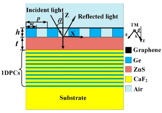
Figure 1.
Schematic diagram of the proposed absorber.
The surface conductivity σs of graphene can be expressed by using the Kubo formula with
where kB is Boltzmann’s constant, τ is the relaxation time, T is the temperature, e is the electron charge, is the reduced Planck’s constant and Ef is the Fermi energy [48]. Thus, the refractive index of graphene can be expressed as with the approximate graphene thickness tg = 0.34 nm and vacuum permittivity ε0. In addition, T and τ are 300 K and 1 ps, respectively.
3. Results and Discussion
To provide efficient reflection with 1DPCs, the optical thickness of each film layer in 1DPCs should be equal to one quarter of the interested wavelength [49]. In addition, to obtain higher reflection with less film layer pairs, the refractive index ratio of two dielectrics in 1DPCs should be large. CaF2 and Ge have little absorption loss in the mid-infrared regime. Furthermore, CaF2 has low refractive indices. Therefore, to achieve high reflection in the mid-infrared regime, we choose CaF2 and Ge as the two primitive dielectrics of 1DPCs, and the thicknesses of the CaF2 and Ge layers are set as tC = 0.55 μm and, tG = 0.31 μm respectively. Other parameters are optimized with p = 2.0 μm, N = 10, w = 1.0 μm, h = 1.0 μm, θ = 0° and t = 1.027 μm. Figure 2a shows that, at Ef = 0.2 eV, there is an absorption peak at the wavelength of 5.14803 μm with a full width half maximum (FWHM) of 0.055 nm, which is much less than those with metallic metamaterials [21,22,23,24,25]. The parameters used in the next parts are the same as those in Figure 2a if they are not specified. Figure 2b shows that the absorption peak can shift from 5.14803 to 5.1411 μm by changing Ef from 0.2 to 0.6 eV.
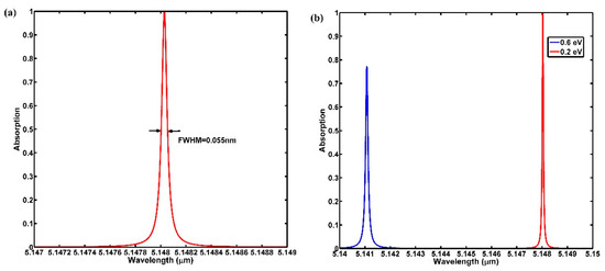
Figure 2.
(a) Absorption spectrum with Ef = 0.2 eV; (b) absorption spectra with Ef = 0.2 eV and Ef = 0.6 eV.
To investigate the influence of the incidence angle on absorption, we plot the absorption spectra with different incidence angles in Figure 3a. As seen in Figure 3a, we can find that the ultra-narrowband resonance absorption exists in two angle regions. One is from 0° to 4°, and the other is from 5° to 8°. To further show the angle-dependent absorption characteristics, we plot the absorption spectra with small angle ranges in Figure 3b,c. From Figure 3b, we can see that the absorption peak shift in the angle range from 0° to 2° is smaller than 0.2 nm, and the absorption rate is still larger than 0.95 for angles up to 2°. Furthermore, the absorption rate decreases drastically in the angle range from 2° to 4°. Figure 3c shows that the absorption peaks will shift to the shorter wavelengths as the incidence angles increase in the angle range from 5° to 8°. In addition, we can see that, in the angle range from 5° to 8°, the resonance absorption rate decreases when the incidence angle deviates from 6°. From the above discussion, we can conclude that the resonance absorption only occurs in a small angle range, which means that our absorber can be used as a mid-infrared thermal source with a near-collimated light beam.
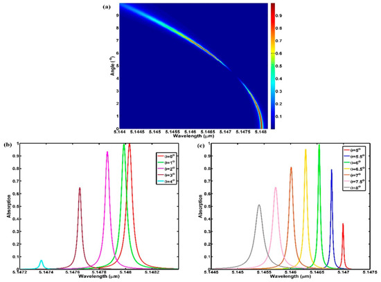
Figure 3.
(a) Absorption spectra with different incidence angles; (b) absorption spectra with incidence angles from 0° to 4°; (c) absorption spectra with incidence angles from 5° to 8°.
To reveal the physical mechanism of the perfect absorption, we calculate the electromagnetic field distributions of and within one-unit cell at the resonance absorption peak of 5.14803 μm in Figure 4. From Figure 4a, we can find that the magnetic field is mainly localized in the Ge microstructure layer, which causes strong magnetic resonance to occur. In addition, the magnetic field distribution in the ZnS film layer exhibits Fabry–Pérot resonance [50] at the absorption peak. Furthermore, the intensity in the 1DPCs from top to bottom decrease to zero; thus, the 1DPCs with 10 pairs of CaF2 and Ge film layer act as a perfect Bragg mirror to totally reflect the incidence light. Figure 4b shows that the electric field is mainly localized at the top-surface of the microstructures where graphene is located. Therefore, due to the electromagnetic resonance in the Ge microstructures and Fabry–Pérot resonance inside the ZnS film layer, near-perfect absorption can be realized.
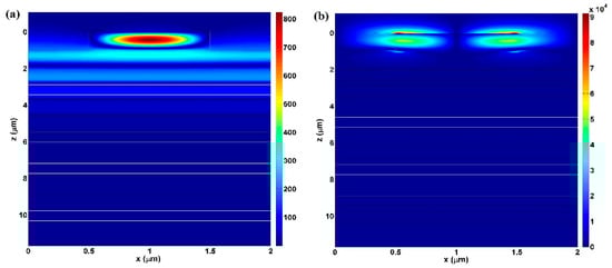
Figure 4.
Field distributions at the resonance absorption wavelength of 5.14803 μm: (a) magnetic field; (b) electric field.
We notice that the optical path in the ZnS layer is approximately equal to the half-resonance wavelength. To further demonstrate the Fabry–Pérot resonance effect, we optimize the ZnS film thicknesses of t = 2.15 μm and t = 3.286 μm with different high-order resonance modes. Figure 5a,b show the absorption spectra with t = 2.15 μm and t = 3.286 μm, respectively. As seen in Figure 5a,b, the absorption bandwidths are narrower than that in Figure 2a. In addition, the bandwidth in Figure 5b is narrower than that in Figure 5a. The magnetic field distributions with t = 2.15 μm and t = 3.286 μm are presented in Figure 5c,d, respectively. The magnetic field distributions in the ZnS film layer indicate the first-order mode and second-order mode in Figure 5c,d, respectively. The results in Figure 5 indicate that the bandwidths can be further narrowed by increasing the thickness of the ZnS film layer, and the related mechanism can be interpreted based on the Fabry–Pérot resonance effect [20]. Based on the Fabry–Pérot resonance theory, the FWHM at the resonance absorption wavelength can be expressed as [50]
where λ0 is the resonance wavelength, , and R1 and R2 are the reflections of the top layer of the ZnS film layer and the 1DPCs, respectively. Equation (2) shows that the FWHM is inversely proportional to the ZnS layer thickness. Thus, an absorber with narrower bandwidth can be realized by adding the thickness of the ZnS film layer.
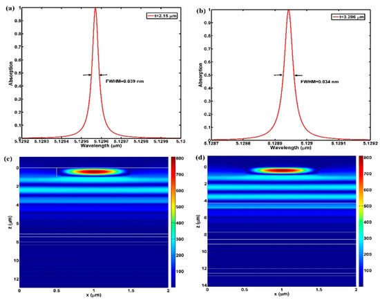
Figure 5.
Absorption spectra with different silica layer thickness: (a) t = 2.15 μm and (b) t = 3.286 μm. Magnetic field distributions: (c) t = 2.15 μm and (d) t = 3.286 μm.
To investigate the influence of the pair layers (N) on the transmission and absorption, we have calculated the spectra of transmission and absorption with different values of N in Figure 6. As seen in Figure 6a, the transmission decreases to zero as N increases from 6 to 10. In addition, the absorption rate increases to 100% as N increases to 10 in Figure 6b, and it maintains a constant value of 100% when N is larger than 10. To reduce computation costs, we set N as 10, which indicates that the 1DPCs can act as a perfect Bragg mirror to provide efficient reflection.
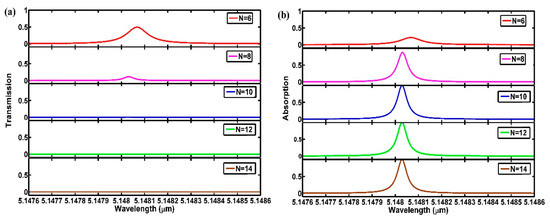
Figure 6.
(a) Transmission spectra with different N; (b) absorption spectra with different N.
Next, we calculate the absorption spectra with the different geometric parameters of w, h and t in Figure 7. As seen in Figure 7a, the absorption rate of the absorber will decrease as w deviates from 1 μm, and it remains above 0.85 as w ranges from 0.994 to 1.006 μm. The absorption spectra with different values of h are shown in Figure 7b. From Figure 7b, we can see that the absorption peaks shift to longer wavelengths as the grating heights increase, and the absorption rate is still larger than 0.8 in the grating height range from 0.98 and 1.02 μm. Figure 7c gives the absorption spectra with different t. As seen in Figure 7c, the resonance absorption peaks shift to the longer wavelengths as the t increases. This phenomenon can be explained by increasing of the optical path g. The above discussion indicates that our proposed structure still has good absorption characteristics if the related parameters only slightly deviate from the optimized values.
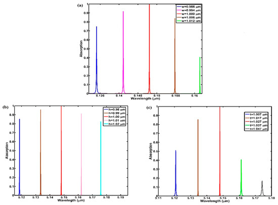
Figure 7.
(a) Absorption spectra with different w; (b) absorption spectra with different h; (c) absorption spectra with different t.
4. Conclusions
A small-angle ultra-narrowband mid-infrared tunable absorber that uses graphene and dielectric metamaterials has been reported. The absorption bandwidth of the absorber at the graphene Fermi level of 0.2 eV is 0.055 nm, and the absorption peaks can be tuned by changing the graphene Fermi level. Furthermore, the resonance absorption only occurs in the angle range of several degrees. The simulation results also show that the bandwidth can be further narrowed by increasing the resonance cavity length. This absorber has potential applications as a tunable near-collimated coherent thermal source.
Author Contributions
Conceptualization, Y.-L.L.; methodology, H.W.; validation, Y.Z.; formal analysis, X.C. and J.W.; investigation, Z.C. All authors have read and agreed to the published version of the manuscript.
Funding
This work is supported by the National Natural Science Foundation of China (No. 51901001), the Anhui Provincial Natural Science Foundation (No. 2008085MF221 and 1908085MF198) and the Provincial Natural Science Foundation of Anhui Higher Education Institution of China (No. KJ2019A0016 and KJ2018A0175).
Institutional Review Board Statement
Not applicable.
Informed Consent Statement
Not applicable.
Data Availability Statement
Data is contained within the article.
Conflicts of Interest
The authors declare no conflict of interest.
References
- Yu, Z.; Veronis, G.; Fan, S.; Brongersma, M.L. Design of midinfrared photodetectors enhanced by surface plasmons on grating structures. Appl. Phys. Lett. 2006, 89, 151116. [Google Scholar] [CrossRef] [Green Version]
- Cai, L.; Li, Q.; Yu, J.; Luo, H.; Du, K.; Qiu, M. Simultaneous single-peak and narrowband thermal emission enabled by hybrid metal-polar dielectric structures. Appl. Phys. Lett. 2019, 115, 093505. [Google Scholar] [CrossRef]
- Li, J.; Chen, X.; Yi, Z.; Yang, H.; Tang, Y.; Yi, Y.; Yao, W.; Wang, J.; Yi, Y. Broadband solar energy absorber based on monolayer molybdenum disulfide using tungsten elliptical arrays. Mater. Today Energy 2020, 16, 100390. [Google Scholar] [CrossRef]
- Cen, C.; Chen, Z.; Xu, D.; Jiang, L.; Chen, X.; Yi, Z.; Wu, P.; Li, G.; Yi, Y. High quality factor, high sensitivity metamaterial graphene-perfect absorber based on critical coupling theory and impedance Matching. Nanomaterials 2020, 10, 95. [Google Scholar] [CrossRef] [PubMed] [Green Version]
- Ji, Y.; Tang, C.; Xie, N.; Chen, J.; Gu, P.; Peng, C.; Liu, B. High-performance metamaterial sensors based on strong coupling between surface plasmon polaritons and magnetic plasmon resonances. Results Phys. 2019, 14, 102397. [Google Scholar] [CrossRef]
- Liao, Y.-L.; Zhao, Y. A wide-angle broadband polarization-dependent absorber with stacked metal-dielectric grating. Opt. Commun. 2016, 370, 245–249. [Google Scholar] [CrossRef]
- Sergeant, N.P.; Pincon, O.; Agrawal, M.; Peumans, P. Design of wide-angle solar-selective absorbers using aperiodic metal-dielectric stacks. Opt. Express 2009, 17, 22800–22812. [Google Scholar] [CrossRef]
- Liao, Y.-L.; Zhao, Y.; Wu, S.; Feng, S. Wide-angle broadband absorber based on uniform-sized hyperbolic metamaterial. Opt. Mater. Express 2018, 8, 2484–2493. [Google Scholar] [CrossRef]
- Wu, D.; Liu, C.; Xu, Z.; Liu, Y.; Yu, Z.; Yu, L.; Chen, L.; Li, R.; Ma, R.; Ye, H. The design of ultra-broadband selective near-perfect absorber based on photonic structures to achieve near-ideal daytime radiative cooling. Mater. Des. 2018, 139, 104–111. [Google Scholar] [CrossRef]
- Liao, Y.-L.; Zhao, Y. Ultrabroadband absorber using a deep metallic grating with narrow slits. Opt. Commun. 2015, 334, 328–331. [Google Scholar] [CrossRef]
- Dayal, G.; Ramarkrishna, A. Design of multi-band metamaterial perfect absorbers with stacked metal–dielectric disksperfect absorbers with stacked metal–dielectric disks. J. Opt. 2013, 15, 055106. [Google Scholar] [CrossRef]
- Wang, B.-X.; He, Y.; Lou, P.; Huang, W.-Q.; Xing, W. Design of a dual-band terahertz metamaterial absorber using two identical square patches for sensing application. Nanoscale Adv. 2020, 2, 763–769. [Google Scholar] [CrossRef] [Green Version]
- Wang, B.-X.; He, Y.; Lou, P.; Huang, W.-Q.; Pi, F. Penta-band terahertz light absorber using five localized resonance responses of three patterned resonators. Results Phys. 2020, 16, 102930. [Google Scholar] [CrossRef]
- Wang, B.-X.; Tang, C.; Niu, Q.; He, Y.; Chen, T. Design of narrow discrete distances of dual/triple-band terahertz met-amaterial absorbers. Nanoscale Res. Lett. 2019, 16, 64. [Google Scholar]
- Cui, Y.; Fung, K.H.; Xu, J.; Ma, H.; Jin, Y.; He, S.; Fang, N.X. ultrabroadband light absorption by a sawtooth anisotropic metamaterial slab. Nano Lett. 2012, 12, 1443–1447. [Google Scholar] [CrossRef] [Green Version]
- Wang, B.-X.; Wang, G.-Z.; Sang, T.; Wang, L.-L. Six-band terahertz metamaterial absorber based on the combination of multiple-order responses of metallic patches in a dual-layer stacked resonance structure. Sci. Rep. 2017, 7, 1–9. [Google Scholar] [CrossRef] [PubMed] [Green Version]
- Long, C.; Yin, S.; Wang, W.; Li, W.; Zhu, J.; Guan, J. Broadening the absorption bandwidth of metamaterial absorbers by transverse magnetic harmonics of 210 mode. Sci. Rep. 2016, 6, 1–9. [Google Scholar] [CrossRef] [PubMed] [Green Version]
- Meng, L.; Zhao, D.; Ruan, Z.; Li, Q.; Yang, Y.; Qiu, M. Optimized grating as an ultra-narrow band absorber or plasmonic sensor. Opt. Lett. 2014, 39, 1137–1140. [Google Scholar] [CrossRef] [PubMed]
- Greffet, J.-J.; Carminati, R.; Joulain, K.; Mulet, J.-P.; Mainguy, S.; Cheng, Y. Coherent emission of light by thermal sources. Nat. Cell Biol. 2002, 416, 61–64. [Google Scholar] [CrossRef] [PubMed]
- Liao, Y.; Zhao, Y. Absorption manipulation in a narrowband infrared absorber based on the hybridization of gap plasmon and fabry-perot resonance. Plasmonics 2015, 10, 1219–1223. [Google Scholar] [CrossRef]
- Zhao, D.; Meng, L.; Gong, H.; Chen, X.; Chen, Y.; Yan, M.; Li, Q.; Qiu, M. Ultra-narrow-band light dissipation by a stack of lamellar silver and alumina. Appl. Phys. Lett. 2014, 104, 221107. [Google Scholar] [CrossRef]
- Meng, L.; Zhao, D.; Yang, Y.; de Abajo, F.J.G.; Li, Q.; Ruan, Z.; Min, Q. Gain-assisted plasmon resonance narrowing and its application in sensing. Phys. Rev. Appl. 2019, 11, 044030. [Google Scholar] [CrossRef] [Green Version]
- Feng, A.; Yu, Z.; Sun, X. Ultranarrow-band metagrating absorbers for sensing and modulation. Opt. Express 2018, 26, 28197–28205. [Google Scholar] [CrossRef]
- He, X.; Jie, J.; Yang, J.; Chen, Y.; Han, Y.; Zhang, S. Suppressing the unwanted resonance mode in a metal-insulator-metal structure using fine-structured gratings. Opt. Express 2019, 27, 15298–15308. [Google Scholar] [CrossRef]
- Li, R.; Wu, D.; Liu, Y.; Yu, L.; Yu, Z.; Ye, H. Infrared plasmonic refractive index sensor with ultra-high figure of merit based on the optimized all-metal grating. Nanoscale Res. Lett. 2017, 12, 1–6. [Google Scholar] [CrossRef] [Green Version]
- Liao, Y.-L.; Zhao, Y.; Zhang, X.; Chen, Z. An ultra-narrowband absorber with a compound dielectric grating and metal substrate. Opt. Commun. 2017, 385, 172–176. [Google Scholar] [CrossRef]
- Liao, Y.; Zhao, Y. An ultra-narrowband absorber with a dielectric-dielectric-metal structure based on guide-mode reso-nance. Opt. Commun. 2017, 382, 307–310. [Google Scholar] [CrossRef]
- Ali, M.O.; Tait, N.; Gupta, S. High-Q all-dielectric thermal emitters for mid-infrared gas-sensing applications. J. Opt. Soc. Am. A 2017, 35, 119–124. [Google Scholar] [CrossRef]
- Liao, Y.; Zhao, Y. Ultra-narrowband dielectric metamaterial absorber for sensing based on cavity-coupled phase reso-nance. Results Phys. 2020, 17, 103072. [Google Scholar] [CrossRef]
- Qin, F.; Chen, Z.; Chen, X.; Yi, Z.; Yao, W.; Duan, T.; Wu, P.; Yang, H.; Li, G.; Yi, Y. A tunable triple-band near-infrared metamaterial absorber based on Au nano-cuboids array. Nanomaterials 2020, 10, 207. [Google Scholar] [CrossRef] [PubMed] [Green Version]
- Li, J.; Chen, Z.; Yang, H.; Yi, Z.; Chen, X.; Yao, W.; Duan, T.; Wu, P.; Li, G.; Yi, Y. Tunable broadband solar energy absorber based on monolayer transition metal dichalcogenides materials using Au nanocubes. Nanomaterials 2020, 10, 257. [Google Scholar] [CrossRef] [Green Version]
- Privitera, S.; Rimini, E.; Zonca, R. Amorphous-to-crystal transition of nitrogen- and oxygen-doped Ge2Sb2Te5 films stud-ied by in situ resistance measurements. Appl. Phys. Lett. 2004, 85, 3044–3046. [Google Scholar] [CrossRef]
- Wang, T.; Zhang, H.; Zhang, Y.; Zhang, Y.; Cao, M. Tunable bifunctional terahertz metamaterial device based on dirac semimetals and vanadium dioxide. Opt. Express 2020, 28, 17434–17448. [Google Scholar] [CrossRef] [PubMed]
- Wang, Y.; Li, T.; Zhu, S. Graphene-based plasmonic modulator on a groove-structured metasurface. Opt. Lett. 2017, 42, 2247–2250. [Google Scholar] [CrossRef]
- Jia, Z.-X.; Shuai, Y.; Xu, S.-D.; Tan, H.-P. Graphene-based tunable metamaterial filter in infrared region. Smart Sci. 2016, 4, 127–133. [Google Scholar] [CrossRef]
- Liao, Y.-L.; Zhao, Y. Graphene-based tunable ultra-narrowband mid-infrared TE-polarization absorber. Opt. Express 2017, 25, 32080–32089. [Google Scholar] [CrossRef]
- Xu, K.; Li, J.; Zhang, A.; Chen, Q. Tunable multi-band terahertz absorber using a single-layer square graphene ring structure with T-shaped graphene strips. Opt. Express 2020, 28, 11482–11492. [Google Scholar] [CrossRef] [PubMed]
- Chen, X.; Tian, Z.; Lu, Y.; Xu, Y.; Zhang, X.; Ouyang, C.; Gu, J.; Han, J.; Zhang, W. Electrically tunable perfect terahertz ab-sorber based on a graphene salisbury screen hybrid metasurface. Adv. Opt. Mater. 2020, 8, 1900660. [Google Scholar] [CrossRef]
- Cai, Y.; Guo, Y.; Zhou, Y.; Huang, X.; Yang, G.; Zhu, J. Tunable dual-band terahertz absorber with all-dielectric configura-tion based on graphene. Opt. Express 2020, 28, 31524–31534. [Google Scholar] [CrossRef]
- Khavasi, A. Ultra-sharp transmission resonances in periodic arrays of graphene ribbons in te polarization. J. Light. Technol. 2015, 34, 1020–1024. [Google Scholar] [CrossRef]
- Chang, J.-H.; Wang, T.-T.; Zhang, C.; Ge, Y.-X.; Tao, Z.-H.; Jian-Hua, C.; Ting-Ting, W.; Chuang, Z.; Yi-Xian, G.; Zai-Hong, T. Compact and tunable mid-ir light source based on a dual-wavelength fiber laser. Chin. Phys. Lett. 2013, 30, 114206. [Google Scholar] [CrossRef]
- Cao, Y.; Hu, E.; Xing, J.; Liu, L.; Gu, T.; Zheng, J.; Yu, K.; Wei, W. Optical constants of restored and etched reduced graphene oxide: A spectroscopic ellipsometry study. Opt. Mater. Express 2018, 9, 234–243. [Google Scholar] [CrossRef]
- Wang, W.; Qu, Y.; Du, K.; Bai, S.; Tian, J.; Pan, M.; Ye, H.; Qiu, M.; Li, Q. Broadband optical absorption based on single-sized metal-dielectric-metal plasmonic nanostructures with high-ε″ metals. Appl. Phys. Lett. 2017, 110, 101101. [Google Scholar] [CrossRef]
- Liao, Y.-L.; Zhao, Y. Ultra-narrowband mid-infrared absorber based on Mie resonance in dielectric metamaterials. Can. J. Phys. 2020, 98, 484–487. [Google Scholar] [CrossRef]
- Moharam, M.G.; Gaylord, T.K.; Grann, E.B.; Pommet, D.A. Formulation for stable and efficient implementation of the rigorous coupled-wave analysis of binary gratings. J. Opt. Soc. Am. A 1995, 12, 1068–1076. [Google Scholar] [CrossRef]
- Amotchkina, T.; Trubetskov, M.; Hahner, D.; Pervak, V. Characterization of e-beam evaporated Ge, YbF3, ZnS, and LaF3 thin films for laser-oriented coatings. Appl. Opt. 2020, 59, A40–A47. [Google Scholar] [CrossRef] [PubMed]
- Malitson, I.H. A redetermination of some optical properties of calcium fluoride. Appl. Opt. 1963, 2, 1103–1107. [Google Scholar] [CrossRef]
- Hanson, G.W. Dyadic Green’s functions and guided surface waves for a surface conductivity model of graphene. J. Appl. Phys. 2008, 103, 064302. [Google Scholar] [CrossRef] [Green Version]
- Winn, J.N.; Fink, Y.; Fan, S.; Joannopoulos, J.D. Omnidirectional reflection from a one-dimensional photonic crystal. Opt. Lett. 1998, 23, 1573–1575. [Google Scholar] [CrossRef] [PubMed]
- Born, M.; Wolf, E. Principles of Optics, 6th ed.; Pergamon Press: New York, NY, USA, 1980. [Google Scholar]
Publisher’s Note: MDPI stays neutral with regard to jurisdictional claims in published maps and institutional affiliations. |
© 2021 by the authors. Licensee MDPI, Basel, Switzerland. This article is an open access article distributed under the terms and conditions of the Creative Commons Attribution (CC BY) license (https://creativecommons.org/licenses/by/4.0/).