Abstract
A method based on acoustic emission (AE) sensing in which two AE sensors are used to measure the tribological characteristics of two interacting friction materials simultaneously in real time was assessed for the in situ measurement and evaluation of the wear process of silver plating. AE sensors were attached to a silver-plated pin and a silver-plated plate, and the two AE signals were measured simultaneously on a pin-on-plate-type reciprocating sliding tester. The resulting changes in the AE signal could be classified into three phases. Surface observations and energy-dispersive X-ray spectroscopy analyses showed that the wear of the silver-plating layer progressed in Phase I, the nickel intermediate layer was exposed and wear of the nickel progressed in Phase II, and the contact electrical resistance increased and the copper substrate was exposed in Phase III. In summary, the wear process of a silver-plating layer, which cannot be identified from the changes in the frictional resistance or the contact electric resistance, can be detected from changes in the dual AE signals. Furthermore, changes in the wear state of both the pin and plate specimens can be identified from differences in the amplitudes of the AE signals and the timing of their detection.
1. Introduction
Friction and wear are basically caused by the interactions of surface asperities on two contacting materials that might have atmospheric gas molecules or lubricants present on their surfaces. The deformation and fracture phenomena that occur between the friction surfaces are complicated and unpredictable. To grasp the state of friction and wear between two friction surfaces with high accuracy, it is necessary to measure and evaluate the surface state of each material by means of measurements made in situ. However, the states of friction surfaces and their amounts of wear are generally evaluated by measurements made ex situ after stopping the operation of the relevant machine. However, if the operation is stopped and the frictional surfaces are separated, their actual state is not maintained. In addition, any deformation or fracture that might occur under the coating layer cannot be seen from the outside [1]. Consequently, because it is not possible to be certain that ex situ measurements provide an accurate assessment of the state of the friction system, an in situ measurement method for evaluating the state of the two frictional materials simultaneously is required instead.
In the case of plated materials used as electrical contacts, although various studies have made on their tribological problems [2,3,4,5,6,7], many aspects of the wear mechanism remain unknown. Because wear progresses through several different stages from the start of wear to the end of the lifetime of a composite material, it is necessary to identify the state of wear for each layer of the material, such as the surface plating, intermediate plating, and substrate, at each stage. Additionally, it is important to know which makes the greater contribution: adhesive wear or abrasive wear. Furthermore, it is necessary to understand any differences between the fixed side and the moving side of an electrical contact. Elucidation of the wear mechanism and a clarification of the effects of various material combinations and terminal shapes would contribute greatly to the development of new materials for electrical contacts.
For terminals of automobile wiring harnesses, which are currently gold plated, a switch to silver plating is being considered as a means of reducing costs [8]. Therefore, the wear mechanism of the silver-plating layer, its intermediate-plating layer, and the substrate need to be examined in detail. In silver plating, which requires high wear resistance, the lifetime of the coating is defined as the period until the nickel of the base plating is exposed. No method for detecting this period has yet been established. Even when the silver layer is partially removed, a low contact electrical resistance is maintained, so the lifetime of silver plating cannot be detected by measuring the contact electrical resistance alone. Similarly, because the friction coefficient fluctuates markedly, it cannot be used as an evaluation parameter. In this study, acoustic emission (AE) sensing, which is a measurement method used to monitor and evaluate the state of a material by detecting and analyzing elastic stress waves generated when the material deforms and fractures, was tested for the evaluation of wear of a silver-plating layer. Various leading-edge studies on AE sensing related to tribology are likely to permit the establishment of in situ measurement and the evaluation of tribological characteristics [9,10,11,12,13]. If AE sensing could be used to detect the lifetime of such a layer, it should be possible to make an accurate evaluation of the correlation between test conditions and durability, permitting efficient research in the development of new products.
In essence, friction and wear phenomena occur between pairs of friction materials, and the surface condition of each of the two materials changes sequentially in a different manner. As mentioned earlier, to evaluate the wear state with high accuracy, it is necessary to measure the state of each friction material in real time. Therefore, in this study we attached an AE sensor to each of two interacting friction materials, and we simultaneously measured the AE waves generated from each material. We have named this novel technique “dual AE sensing”. Although many studies on source location by using multiple AE sensors have been conducted [14,15,16,17], our present approach is unprecedented. We hoped that by monitoring changes in the amplitudes of AE signals and detecting the timing of bursts of AE by dual AE sensing, it would be possible to perform in situ measurement and to make an accurate evaluation of the state of wear of each plating layer. Our sliding friction experiments with dual AE sensing were performed with silver-plated pin-and-plate test pieces, and we assessed whether the wear states of the plating layers on both test pieces could be measured and evaluated.
2. Materials and Methods
Figure 1 shows the appearance of our test equipment and Figure 2 is a schematic representation of the pin-on-plate type reciprocating sliding tester that we used in this study. With this tester, the normal force and frictional force were measured by using load cells. At the same time, the contact electrical resistance between the two specimens was measured by the four-terminal method at an applied constant current of 10 mA. The experiments were conducted by attaching an embossed specimen to the upper part (pin side) of the tester and attaching a plate specimen to the stage. As shown in Figure 1 and Figure 2, a wideband-type AE sensor was installed on the jig to which the embossed specimen was fixed, and an identical sensor was attached to the plate specimen. An instant glue was used to attach the sensors. The optimal positions for attaching the AE sensors to the two specimens were determined by means of a preliminary experiment in which the AE signal amplitudes at various positions were compared. Table 1 shows the AE measurement conditions. The output signals from the two AE sensors were amplified with an amplification factor of 90 dB and were passed through a high-pass filter (50 kHz or 100 kHz) to eliminate noise. The AE signals were evaluated in terms of the AE mean amplitude, i.e., the amplitude of the voltage signal after passage through half-wave rectification, an enveloping process, and an averaging process with a discriminator after the filter.
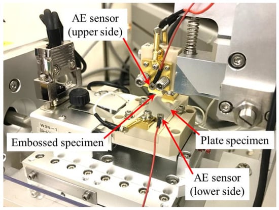
Figure 1.
Appearance of the experimental setup.
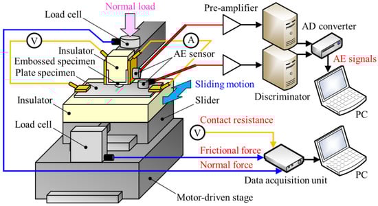
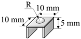
Figure 2.
Schematic diagram of the experimental setup and the measurement system.

Table 1.
Summary of the AE measurement conditions.
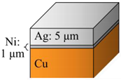
Table 2 shows the details of the specimens and the sliding conditions that we used in our study. The pin specimen was an embossed specimen with a hemispherical protrusion of radius (R) 1.5 mm. The pin and plate specimens had a total thickness of 0.64 mm and consisted of a copper substrate with a layer of matte nickel plating [thickness (t) = 1 µm] surmounted by a glossy silver plating (t = 5 µm). In some experiments, an embossed protrusion of R = 1.0 mm on a plate of thickness of 0.2 mm (silver plating thickness: 1 µm; nickel plating thickness: 0.5 µm) was used. Nickel plating plays a role in preventing the substrate or any lower layer of plating material from diffusing into the upper layer. The friction and wear experiments were conducted with a normal load of 3.0 N and sliding velocities of 100 mm/min or 200 mm/min, with a reciprocating sliding distance of 5 mm. The thickness of specimens, the normal load, and the sliding velocity were varied to change the wear process for each plating layer in the electric-contact material in a stepwise manner. All experiments were performed at room temperature in the open air without lubrication.
Table 2.
Summary of the specimens and the sliding conditions.
3. Results and Discussion
3.1. Series of Wear Processes for the Silver-Plating Layer
First of all, we will give an overview of the series of wear processes of the silver-plating layer as identified by the friction and wear experiments. Figure 3 shows the changes in the frictional force and the corresponding contact electrical resistance for an experiment involving 50 reciprocation cycles for specimens with a silver-plating thickness of 1 µm. The average one-way sliding period for the frictional force and the contact electrical resistance were calculated and plotted as “going” and “returning” data. Here, it is inferred that the difference between the frictional force values for the “going” and “returning” strokes was the result of differences in the rigidity of the embossed specimen fixing arm. The frictional force temporarily increased immediately after the start of sliding, and then decreased gradually through a running-in process. The frictional force subsequently increased at about the 30th reciprocation. The contact electrical resistance also initially decreased due to the effect of the running-in process, but then increased from the 25th reciprocation, before the frictional force increased.
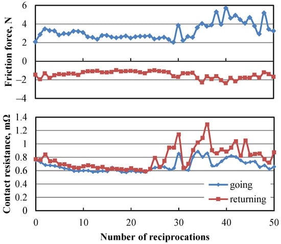
Figure 3.
Changes in the frictional force and the electrical contact resistance (t = 0.2 mm, Ag plating 1 µm, v = 100 mm/min).
Figure 4 shows micrographs of the worn surface of both specimens after 50 reciprocation cycles. The surface was found to be roughened due to adhesion and the presence of residues of transfer particles, and it can be seen that the copper of the substrate was exposed in both specimens. During the experiment, metallic-colored severe-wear particles, as shown in Figure 5, were also observed. An enlarged image of the surface of the wear particles (Figure 5b) showed the presence of both copper and silver-colored parts. These particles were therefore generated through a mutual transfer-and-growth process due to adhesive wear [18,19].
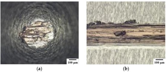
Figure 4.
Micrographs of the worn surfaces of a (a) the embossed specimen and (b) the plate specimen (t = 0.2 mm, Ag plating 1 µm, v = 100 mm/min, n = 50).
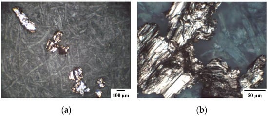
Figure 5.
Micrographs of wear particles collected after the experiment: (a) the shape and (b) the surface.
3.2. Change in the AE Signals Due to Wear of the Silver-Plating Layer
Next, we examined changes in the AE signal due to the wear process for the silver-plating layer, as described above.
3.2.1. Changes in AE Signal for the Plate Specimen
First, the change in the AE signal for the plate specimen will be discussed. Figure 6, Figure 7 and Figure 8 show the experimental results obtained by using specimens with a silver-plating thickness of 5 µm. Figure 7 shows changes in the AE mean amplitude detected from the plate-specimen side, corresponding to the experiment in Figure 6. It can be seen from the results in Figure 6 that the changes in the frictional force and the contact electrical resistance became stable late in the running-in process. Observations of the worn surface (Figure 8) showed the presence of silver-white transfer particles on the plate specimen and silver-white adhesions on the embossed specimen. Measurements of the cross-sectional shape of the wear track on the plate specimen showed that the wear depth was about 5 µm, and it appears that a silver-plating layer remained in some places only. We therefore consider that the contact electrical resistance did not increase due to the presence of the underlying nickel-plating layer. Local exposure of copper was also observed in areas with deep wear tracks. Therefore, if exposure of copper was not clear, as shown in Figure 4, the frictional force and the contact electrical resistance did not increase significantly. As shown in Figure 7, the change in the AE mean value during the wear process of the silver-plating layer (including the underlying nickel-plating layer) did not produce a loud burst-type AE signal, unlike the case when the copper substrate was exposed. The AE signal amplitude increased slightly as wear progressed. Furthermore, the small burst-type AE signals seen toward the latter half of the experiment are considered to have been due to the growth of small transfer particles.
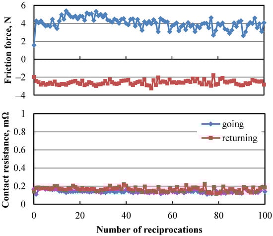
Figure 6.
Changes in the frictional force and the contact electrical resistance (t = 0.64 mm, Ag plating 5 µm, v = 200 mm/min).
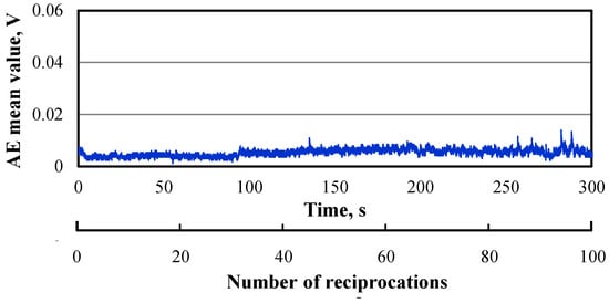
Figure 7.
Changes in the AE mean amplitude measured by the AE sensor for the plate-specimen side, corresponding to the experimental results in Figure 6 (high-pass filter: 100 kHz).
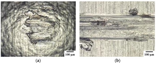
Figure 8.
Micrographs of the worn surfaces of (a) the embossed specimen and (b) the plate specimen (t = 0.64 mm, Ag plating 5 µm, v = 200 mm/min, n = 100 times).
Figure 9, Figure 10 and Figure 11 show the experimental results obtained for a silver-plating thickness of 1 µm, which were similar to the results described in Section 3.1. Figure 10 shows the change in the AE mean value detected from the plate-specimen side, which corresponded to the experiment shown in Figure 9. In the period from 0 to 20 s (the 1st to 3rd reciprocation) in Figure 10, the silver-plating layer appeared to remain on the sliding surface in a manner consistent with the results shown in Figure 6, Figure 7 and Figure 8. The micrographs of the worn surfaces in Figure 11 show that copper was exposed on the surface of the plate specimen and adhesion could be observed on the surface of the embossed specimen. We consider that the sliding surface became rough due to this exposure of the copper substrate, and that the contact electrical resistance and the frictional force increased as a consequence.
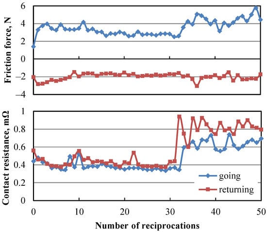
Figure 9.
Changes in the frictional force and the contact electrical resistance (t = 0.2 mm, Ag plating 1 µm, v = 200 mm/min).
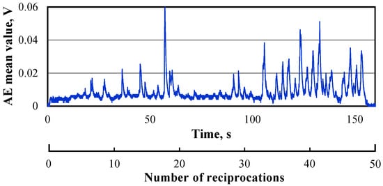
Figure 10.
Changes in the AE mean amplitude measured by the AE sensor for the plate-specimen side, corresponding to the experimental data in Figure 9 (high-pass filter: 100 kHz).
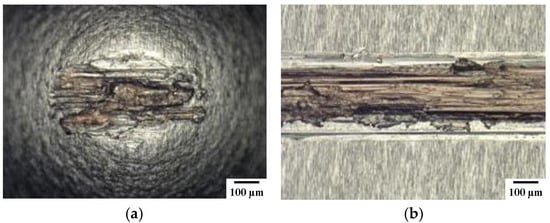
Figure 11.
Micrographs of the worn surfaces of (a) the embossed specimen and (b) the plate specimen (t = 0.2 mm, Ag plating 1 µm, v = 200 mm/min, n = 50 times).
The transition point at around the 30th reciprocation, as shown in Figure 9, corresponds to the time position of 100 s in Figure 10. Therefore, the contact electrical resistance tends to change after the AE signal has changed. This is because AE sensing can capture microscopic wear processes. Even in experiments under different sliding conditions of normal load and sliding velocity, it was confirmed that the contact electrical resistance tended to increase after the burst-type AE signal was temporarily activated. This change in the AE mean value is considered to have corresponded to activation of the burst-type AE signal due to the mutual transfer-and-growth process, and the decrease was due to the detachment of transfer particles [20].
3.2.2. Changes in AE Signal for the Embossed-Specimen Side
In this section, changes in the AE signal for the embossed-specimen side are described and two typical sets of results obtained from sliding experiments with 50 reciprocations with a silver-plating thickness of 1 µm are presented. The changes in the frictional force and the contact electrical resistance were almost the same as those in Figure 3 and Figure 9, so they are omitted. Figure 12 shows the changes in the AE mean value as measured by the AE sensor for the embossed-specimen side. The difference in the AE signal level between these two experimental results is considered to have arisen from differences in the progress of wear.
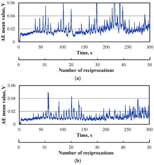
Figure 12.
Changes in the AE mean amplitude value as measured by the AE sensor for the embossed-specimen side (t = 0.2 mm, Ag plating 1 µm, v = 100 mm/min, n = 50 times, high-pass filter: 100 kHz): (a) Experiment 1 and (b) Experiment 2.
Figure 13 shows micrographs of the worn surfaces of the embossed specimens for (a) Experiment 1 and (b) Experiment 2. From observations of the wear surface and measurements of the shape of the cross-section of the wear track after the experiments, it was confirmed that there was a difference in damage, especially in the width of the wear track (wear volume), which was larger in Experiment 1. Consequently, as shown in Figure 12a, in Experiment 1, a large burst-type AE signal was detected earlier than in Experiment 2 (Figure 12b). In addition, we found that the change in the AE signal on the embossed-specimen side tended to increase in the latter half, unlike the change in the AE signal from the AE sensor attached to the plate-specimen side. It is likely that this signal captured the progression of damage on the embossed-specimen side due to repeated rubbing. Because the AE signal amplitude changed with the amount of transfer, we consider that the changes in the AE signal corresponded to various phases of the mutual transfer-and-growth process for each plating layer.
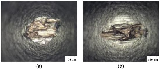
Figure 13.
Micrographs of the worn surface for the embossed specimens corresponding to the experimental data in Figure 12: (a) Experiment 1 and (b) Experiment 2.
3.3. Phase of Wear Based on Changes in the AE Signal
Figure 14 shows the changes in the frictional force, the contact electrical resistance, and the AE mean value obtained in sliding experiments with 150 reciprocations and a silver-plating thickness of 5 µm. It was confirmed that the frictional force increased from around the 100th reciprocation and that large fluctuations were finally observed. The contact electrical resistance rose after the 96th reciprocation, before the frictional force increased. This is thought to because the copper of the substrates was exposed and adhesive wear between the copper layers took place, causing significant roughening of the sliding surfaces. With regard to the AE measurement conditions, the AE high-pass filter was changed from 100 kHz to 50 kHz to take account of the fact that the AE signals originated from frictional phenomena [21]. The changes in the two AE signals from the two sensors were basically similar but differed in some respects. These differences in timing and the amplitude of the AE signals are considered to have captured differences in the progress of plastic deformation and the transfer phenomena on the two surfaces. In addition, burst-type AE signals were detected at about the 20th reciprocation, and therefore the AE measurements captured phenomena in the early stages of wear that were difficult to identify from changes in the frictional force or the contact electrical resistance.
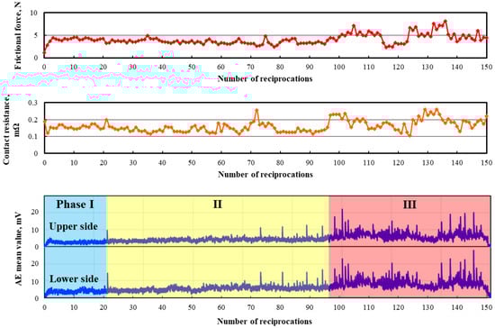
Figure 14.
Changes in the frictional force, contact electrical resistance and AE signals for the three phases of wear (t = 0.64 mm, Ag plating 5 µm, v = 200 mm/min, HPF: 50 kHz).
The progress of wear was classified into the following three phases based on changes in the AE signals.
- Phase I: Region where no large burst-type AE signals were detected.
- Phase II: Region where large burst-type AE signals were detected and the fluctuations gradually increased.
- Phase III: Region where large burst-type AE signals were actively detected and large fluctuations appeared.
To clarify the differences between the various phases, the experiment was stopped at the beginning of Phase I and Phase II, and the wear surface was analyzed by energy-dispersive X-ray spectroscopy (EDS) (Figure 15). From the result of the elemental mapping shown in Figure 15a, it can be seen that the outermost surface in Phase I consisted entirely of silver. On the other hand, when the experiment was stopped at the beginning of Phase II, nickel of the intermediate plating was present on microscopic areas, as shown in Figure 15b. Therefore, the burst-type AE signal that was detected was caused by material transfer in adhesive wear. Because the test was stopped when a large burst-type AE signal was detected from the plate specimen side at an early stage of Phase II, the AE signal was detected when the material was transferred from the plate specimen to the embossed specimen.
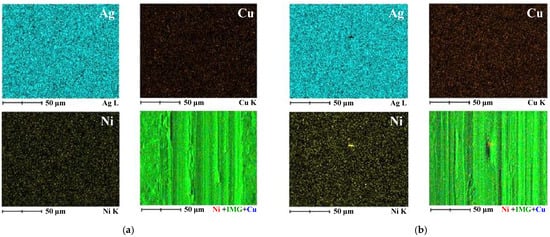
Figure 15.
Elemental mapping images by EDS analysis of the worn surfaces of plate specimens obtained in (a) Phase I and (b) the beginning of Phase II.
The above results and discussion show that the wear process of the plating layer could be identified by using dual-AE sensing. Because each AE pulse wave was generated by material transfer (adhesion and breakdown) [22], the amount of wear for each coating material can be estimated by integration of the relevant AE pulse waves.
4. Conclusions
In this study of pin-on-plate-type reciprocating sliding, two AE sensors were attached to silver-plated embossed and plate specimens, respectively, to verify the usefulness of dual sensing of AE signals. Our conclusions from this study are as follows.
- The AE signal changes before the frictional force or the contact electrical resistance increases.
- When the burst-type AE signal decreases immediately after it has been temporarily activated, the contact electrical resistance tends to increase.
- Changes in two AE signals simultaneously detected from the two specimens show basically the same trends, but there are some variations due to differences in the degree of material transfer and plastic deformation of the sliding surfaces.
- The changes in the AE signals can be classified into three phases. By surface observations and EDS analyses, we confirmed that the wear process of a silver-plating layer progresses in Phase I, the nickel intermediate layer is exposed and the wear of nickel progresses in Phase II, and the copper substrate is exposed and contact electrical resistance increases in Phase III.
- Dual AE sensing can identify wear of a silver-plating layer on both pin and plate specimens that cannot be identified from changes in the frictional force or the contact electrical resistance.
Author Contributions
Conceptualization, A.H. and K.S.; methodology, A.H., Y.S. and K.S.; software, A.H.; validation, A.H. and Y.S.; formal analysis, A.H. and Y.S.; investigation, A.H., Y.S., K.S. and K.A.; resources, A.H., Y.S., K.S. and K.A.; data curation, A.H. and Y.S.; writing—original draft preparation, A.H.; writing—review and editing, A.H.; visualization, A.H.; supervision, A.H. and K.A.; project administration, A.H., Y.S. and K.S.; funding acquisition, A.H. All authors have read and agreed to the published version of the manuscript.
Funding
This research was partly supported by the Japan Society for the Promotion of Science (JSPS) [Grant-in-Aid for Scientific Research (C), No. 19K04154].
Institutional Review Board Statement
Not applicable.
Informed Consent Statement
Not applicable.
Data Availability Statement
The data that support the findings of this study are available from the corresponding author upon reasonable request.
Acknowledgments
The authors thank Souma Yamanaka, who was a student of Saitama Institute of Technology when the experiments were performed, for his assistance.
Conflicts of Interest
The authors declare no conflict of interest.
References
- Mishina, H. Microscopic real time observation of failure, wear and deformation on coating/subsurface. Tribol. Int. 1999, 32, 137–144. [Google Scholar] [CrossRef]
- Beake, B.D.; Harris, A.J.; Liskiewicz, T.W.; Wagner, J.; McMaster, S.J.; Goodes, S.R.; Neville, A.; Zhang, L. Friction and electrical contact resistance in reciprocating nano-scale wear testing of metallic materials. Wear 2021, 474–475, 203866. [Google Scholar] [CrossRef]
- Liskiewicz, T.W.; Kubiak, K.J.; Mann, D.L.; Mathia, T.G. Analysis of surface roughness morphology with TRIZ methodology in automotive electrical contacts: Design against third body fretting-corrosion. Tribol. Int. 2020, 143, 106019. [Google Scholar] [CrossRef]
- Kure-Chu, S.; Nakagawa, R.; Ogasawara, T.; Yashiro, H.; Sawada, S.; Shimizu, A.; Saitoh, Y. Sliding friction, wear and tribofilm formation of silver films electro-plated on copper alloy sheets. In Proceedings of the 2016 IEEE 62nd Holm Conference on Electrical Contacts, Clearwater Beach, FL, USA, 9–12 October 2016; IEEE: Piscataway, NJ, USA, 2016; pp. 135–140. [Google Scholar] [CrossRef]
- Song, J.; Wang, L.; Zibart, A.; Koch, C. Corrosion protection of electrically conductive surfaces. Metals 2012, 2, 450–477. [Google Scholar] [CrossRef]
- Ossart, F.; Noel, S.; Alamarguy, D.; Correia, S.; Gendre, P. Electromechanical modelling of multilayer contacts in electrical connectors. In Proceedings of the 53th IEEE Holm Conference on Electrical Contacts, Pittsburgh, PA, USA, 16–19 September 2007; IEEE: Piscataway, NJ, USA, 2007; pp. 1–8. [Google Scholar] [CrossRef]
- Queffelec, J.L.; Jemaa, N.B.; Travers, D.; Pethieu, G. Materials and contact shape studies for automobile connector development. In Proceedings of the 36th IEEE Conference on Electrical Contacts, and the Fifteenth International Conference on Electrical Contacts, Montreal, QC, Canada, 20–24 August 1990; IEEE: Piscataway, NJ, USA, 1990; pp. 225–231. [Google Scholar] [CrossRef]
- Kloch, K.T.; Kozak, P.; Mlyniec, A. A review and perspectives on predicting the performance and durability of electrical contacts in automotive applications. Eng. Fail. Anal. 2021, 121, 105143. [Google Scholar] [CrossRef]
- König, F.; Sous, C.; Ouald Chaib, A.; Jacobs, G. Machine learning based anomaly detection and classification of acoustic emission events for wear monitoring in sliding bearing systems. Tribol. Int. 2021, 155, 106811. [Google Scholar] [CrossRef]
- Rastegaev, I.; Merson, D.; Rastegaeva, I.; Vinogradov, A. A time-frequency based approach for acoustic emission assessment of sliding wear. Lubricants 2020, 8, 52. [Google Scholar] [CrossRef]
- Shanbhag, V.V.; Rolfe, B.F.; Pereira, M.P. Investigation of galling wear using acoustic emission frequency characteristics. Lubricants 2020, 8, 25. [Google Scholar] [CrossRef]
- Fuentes, R.; Dwyer-Joyce, R.S.; Marshall, M.B.; Wheals, J.; Cross, E.J. Detection of sub-surface damage in wind turbine bearings using acoustic emissions and probabilistic modelling. Renew. Energy 2020, 147, 776–797. [Google Scholar] [CrossRef]
- Hase, A. Early detection and identification of fatigue damage in thrust ball bearings by an acoustic emission technique. Lubricants 2020, 8, 37. [Google Scholar] [CrossRef]
- Ito, K.; Kusano, M.; Demura, M.; Watanabe, M. Detection and location of microdefects during selective laser melting by wireless acoustic emission measurement. Addit. Manuf. 2021, 40, 101915. [Google Scholar]
- Mao, W.; Aoyama, S.; Towhata, I. A study on particle breakage behavior during pile penetration process using acoustic emission source location. Geosci. Front. 2020, 11, 413–427. [Google Scholar] [CrossRef]
- Morscher, G.N.; Han, Z. Damage determination in ceramic composites subject to tensile fatigue using acoustic emission. Materials 2018, 11, 2477. [Google Scholar] [CrossRef] [PubMed]
- Suzuki, T.; Shiotani, T.; Ohtsu, M. Evaluation of cracking damage in freeze-thawed concrete using acoustic emission and X-ray CT image. Constr. Build. Mater. 2017, 136, 619–626. [Google Scholar] [CrossRef]
- Sasada, T.; Norose, S. The formation and growth of wear particles through mutual material transfer. In Proceedings of the Joint JSLE–ASLE International Lubrication Conference, Tokyo, Japan, 9–11 June 1975; Sakurai, T., Ed.; Elsevier: Amsterdam, The Netherlands, 1976; pp. 82–91. [Google Scholar]
- Hase, A.; Mishina, H. Wear elements generated in the elementary process of wear. Tribol. Int. 2009, 42, 1684–1690. [Google Scholar] [CrossRef]
- Hase, A.; Mishina, H.; Wada, M. Acoustic emission in elementary processes of friction and wear: In-situ observation of friction surface and AE signals. J. Adv. Mech. Des. Syst. Manuf. 2009, 3, 333–344. [Google Scholar] [CrossRef]
- Hase, A.; Wada, M.; Mishina, H. Scanning electron microscope observation study for identification of wear mechanism using acoustic emission technique. Tribol. Int. 2014, 72, 51–57. [Google Scholar] [CrossRef]
- Hase, A.; Mishina, H.; Wada, M. Microscopic study on the relationship between AE signal and wear amount. Wear 2013, 308, 142–147. [Google Scholar] [CrossRef]
Publisher’s Note: MDPI stays neutral with regard to jurisdictional claims in published maps and institutional affiliations. |
© 2021 by the authors. Licensee MDPI, Basel, Switzerland. This article is an open access article distributed under the terms and conditions of the Creative Commons Attribution (CC BY) license (https://creativecommons.org/licenses/by/4.0/).