Article

MOCVD Growth of GeTe/Sb2Te3 Core–Shell Nanowires

1
CNR—Institute for Microelectronics and Microsystems, Via C. Olivetti 2, 20864 Agrate Brianza, Italy
2
CNR—Institute for Microelectronics and Microsystems, Via Gobetti, 101, 40129 Bologna, Italy
3
CNR—Institute for Microelectronics and Microsystems, Via del Fosso del Cavaliere, 100, 00133 Rome, Italy
4
CNR—Institute for Microelectronics and Microsystems, Strada VIII, 5, 95121 Catania, Italy
*
Authors to whom correspondence should be addressed.
Coatings 2021, 11(6), 718; https://doi.org/10.3390/coatings11060718
Submission received: 27 April 2021 / Revised: 9 June 2021 / Accepted: 12 June 2021 / Published: 15 June 2021

Abstract

:
We report the self-assembly of core–shell GeTe/Sb2Te3 nanowires (NWs) on Si (100), and SiO2/Si substrates by metalorganic chemical vapour deposition, coupled to the vapour–liquid–solid mechanism, catalyzed by Au nanoparticles. Scanning electron microscopy, X-ray diffraction, micro-Raman mapping, high-resolution transmission electron microscopy, and electron energy loss spectroscopy were employed to investigate the morphology, structure, and composition of the obtained core and core–shell NWs. A single crystalline GeTe core and a polycrystalline Sb2Te3 shell formed the NWs, having core and core–shell diameters in the range of 50–130 nm and an average length up to 7 µm.

1. Introduction

Interest in chalcogenide nanowires (NWs) continues to grow due to their potential capacity to undergo low energy crystalline-amorphous (order-disorder) phase transition [1,2], for several applications such as memory, logic, and sensor devices [3,4,5,6,7,8,9]. Such phase change materials have attracted significant attention, being a promising media for non-volatile phase-change memories (PCM), in addition to optical memories such as (re)writable compact discs (CD) and digital video discs (DVD) [10,11,12]. The realization of PCM devices is, however, still limited due to the requirements of alloy composition, structure, small cell size, high scalability, and low power consumption. The major setback for attaining high-density PCM devices is the operation currents and power consumption needed to prepare the system in the amorphous physical state associated with high resistance reset state [13]. The reduction of the operation currents is desirable because it can realize faster amorphization of material with less power consumed and enable higher storage density, faster memory switching, and higher reliability.
These challenges motivated the researchers to employ bottom-up approaches to synthesize chalcogenide NWs with small diameters [14,15,16]. Moreover, the ability to synthesize such types of NWs facilitates systematic and direct-access studies of size dependence of PCM switching and phase-transition behavior down to sub-lithographic dimensions [13,17]. Recently, self-assembled, single-crystalline GeTe [17,18,19,20], Ge-Sb-Te [15,21], Sb2Te3 [18,22], In3Sb1Te2 [23], In-Sb [24] and In2Se3 [25] NWs have gained much interest in the field of PCM. Advantages of employing NWs for such applications are due to their low dimensionality and single-crystalline, defect-free structure, where novel properties are expected to originate by modifying the essential compositions, sizes, and structures, as in the case of axial [26,27], radial (core–shell) [28,29,30] or branched heterostructured [31] NWs. Core–shell NWs formed by two chalcogenide materials with different phase-change characteristics, namely Ge2Sb2Te5 and GeTe, have been proposed as multi-level PCM memory cells [30]. Compared to Ge2Sb2Te5 and GeTe alloys, Sb2Te3 exhibits lower crystallization temperature and faster reversible switching, making it an ideal candidate for the realization of heterostructure-based multilevel PCM cells, in which the opposite properties of the involved materials can be combined to improve the overall performances, and for carrying out fundamental studies on the role of the heterointerface in the resistive switch. Indeed, the multilevel switching of Ge2Sb2Te5/Sb2Te3 and GeTe/Sb2Te3 PCM cells has been reported for the stacked thin-film geometry [32,33]. However, until now, the growth and nanoscale characterization of GeTe/Sb2Te3 core–shell NWs have not been investigated.
Here, we report for the first time, to our knowledge, the Metalorganic Chemical Vapour Deposition (MOCVD) synthesis of GeTe/Sb2Te3 core–shell NWs. These heterostructures were obtained in two steps: the growth of axial GeTe NWs by vapour–liquid–solid (VLS) process, catalyzed by Au nanoparticles (NPs), was followed by the deposition of a conformal Sb2Te3 shell at room temperature. We explored the different growth conditions and studied the morphological, structural, and compositional properties of the synthesized GeTe/Sb2Te3 NWs.

2. Experimental Section

The growth of the NWs was performed with an Aixtron AIX200/4 MOCVD reactor (Aixtron SE, Herzogenrath, Germany), employing the VLS mechanism induced by Au NPs with average diameter sizes of 10, 20, 30, and 50 nm, respectively. The Au NPs were dispersed from a colloidal solution by Ted Pella © on Si (100) and Si/SiO2 substrates by a simple drop-casting method. For the growth on Si (100) substrates, the native oxide was removed prior to dispersion of the Au NPs by immersion in an HF 5% solution. The employed metalorganic precursors were electronic-grade tetrakisdimethylamino germanium (Ge[N(CH3)2]4, TDMAGe), diisopropyltelluride ((C3H7)2Te, DiPTe), antimonytrichloride (SbCl3), and bis(trimethylsilyl) telluride (Te(SiMe3)2, DSMTe), transported to the MOCVD reactor by an ultra-purified N2 carrier/process gas. The GeTe core NWs were obtained with the reactor temperature (T), reactor pressure (P), and growth duration (t) varied in the range of 300–400 °C, 50–300 mbar, and 60–120 min, respectively. The MOCVD growth of the Sb2Te3 shell over the GeTe core NWs was carried out at room temperature.
The morphology of the NWs was studied by a Zeiss Supra 40 field emission scanning electron microscope (SEM), (Cark Zeiss, Oberkochen, Germany) in both plan and cross-section mode. The structural analysis was performed by X-ray diffraction (XRD) experiments, using an ItalStructures HRD3000 diffractometer system (Ital Structures Sas, Riva de Garda, Italy) to evaluate the average crystal structure of the NWs. The experimental XRD curves were analyzed by a best-fit procedure based on the Rietveld method [34]. The vibrational properties of the NWs were also studied by collecting Raman maps with a Thermo Scientific DXR2xi Raman Imaging Microscope (ThermoFischer Scientific, Waltham, MA, USA), equipped with a 50× objective and a 532 nm excitation laser. The maps were acquired with a step size of 0.5 µm, and each point spectrum resulted from 40 accumulations of 50 ms acquisitions. The local microstructure, growth direction, and composition were studied by high-resolution transmission electron microscopy (HR-TEM). To make the NWs suitable for TEM observations, the as-grown NWs were transferred directly from the substrate by mechanical rubbing on the TEM grid. TEM analyses were performed on a Cs-probe-corrected TEM JEOL ARM200CF microscope (JEOL Ltd, Akishima, Japan), operated in scanning mode, Scanning Transmission Electron Microscope (STEM) at a primary beam energy of 200 keV and equipped with a GIF Quantum ER energy filter by GATAN for electron energy loss spectroscopy (EELS), (Gatan Inc., Pleasanton, CA, USA) spectroscopy.

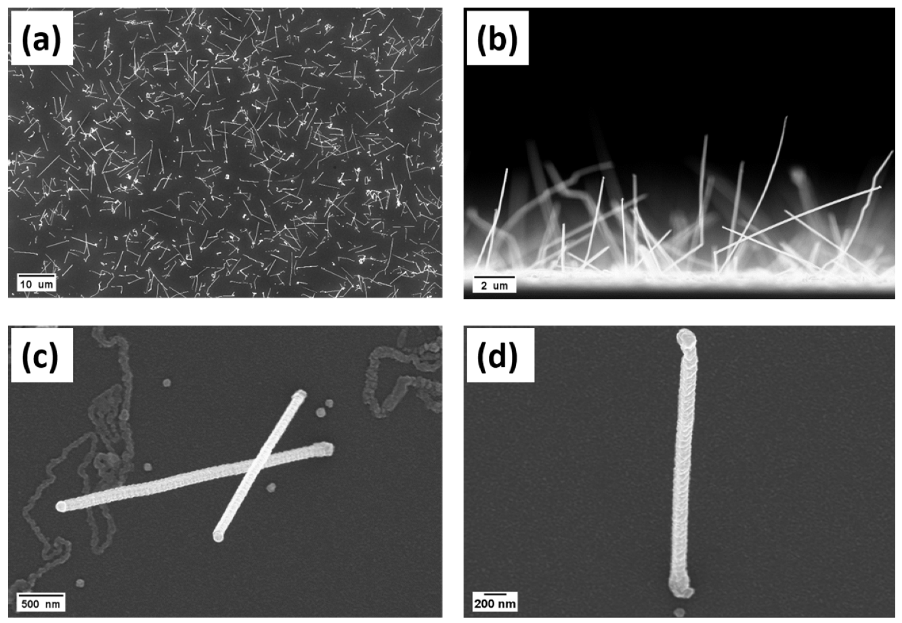
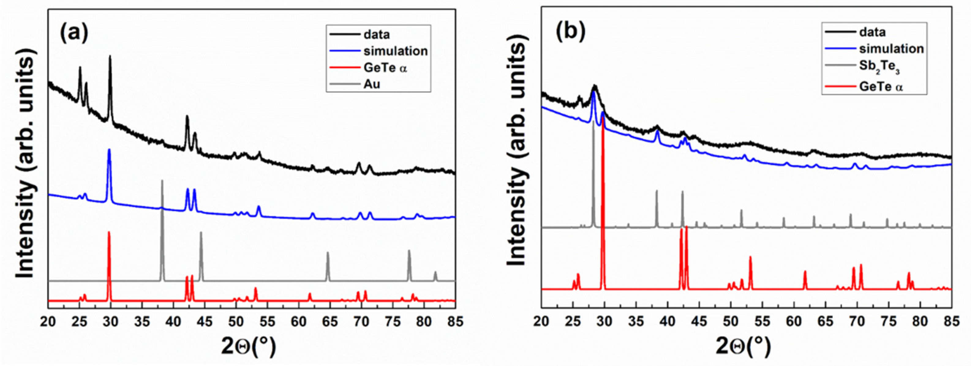
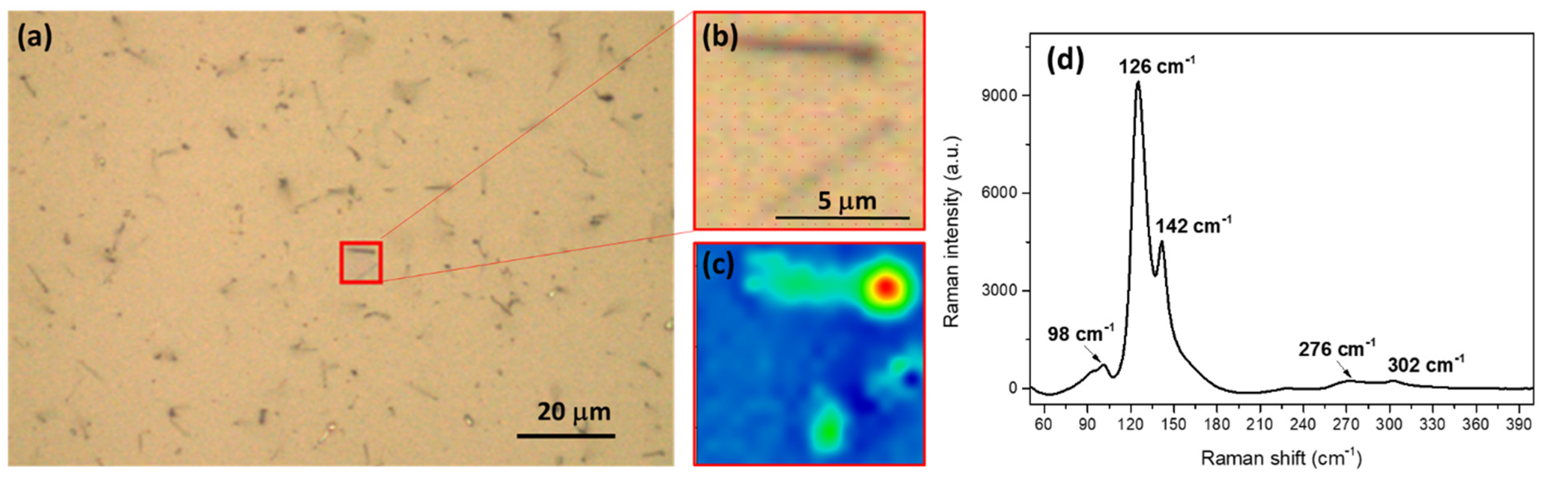
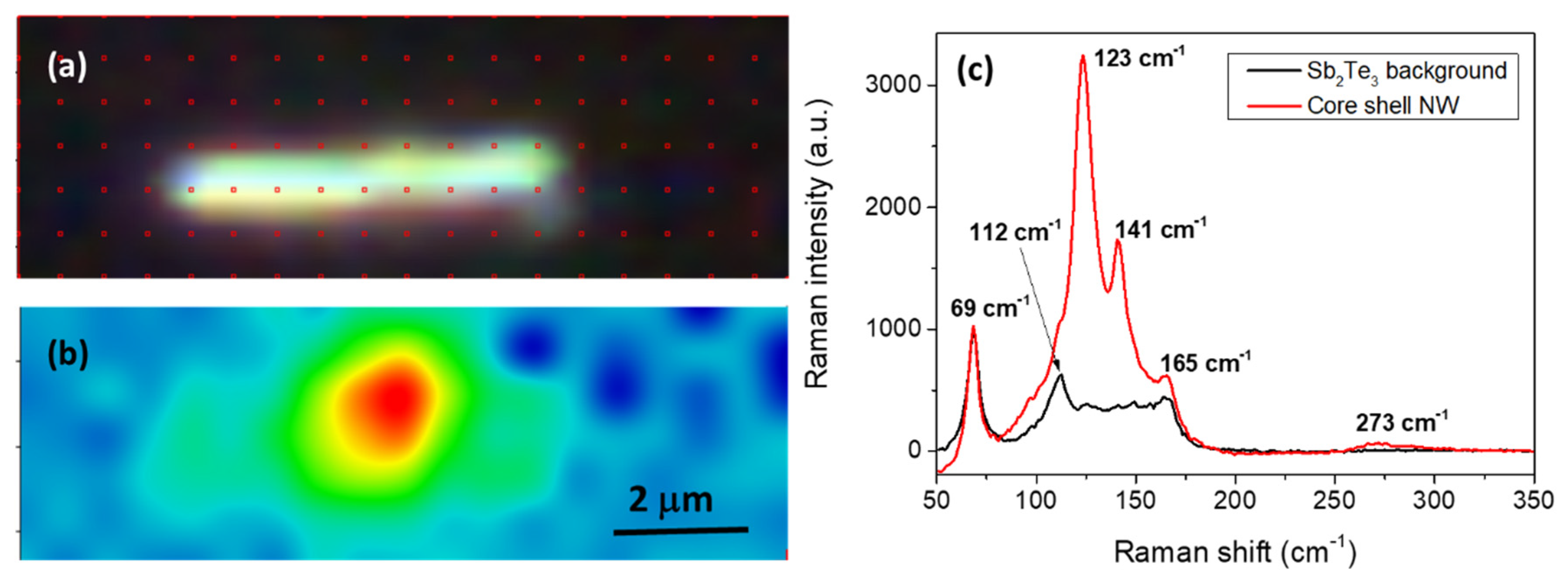
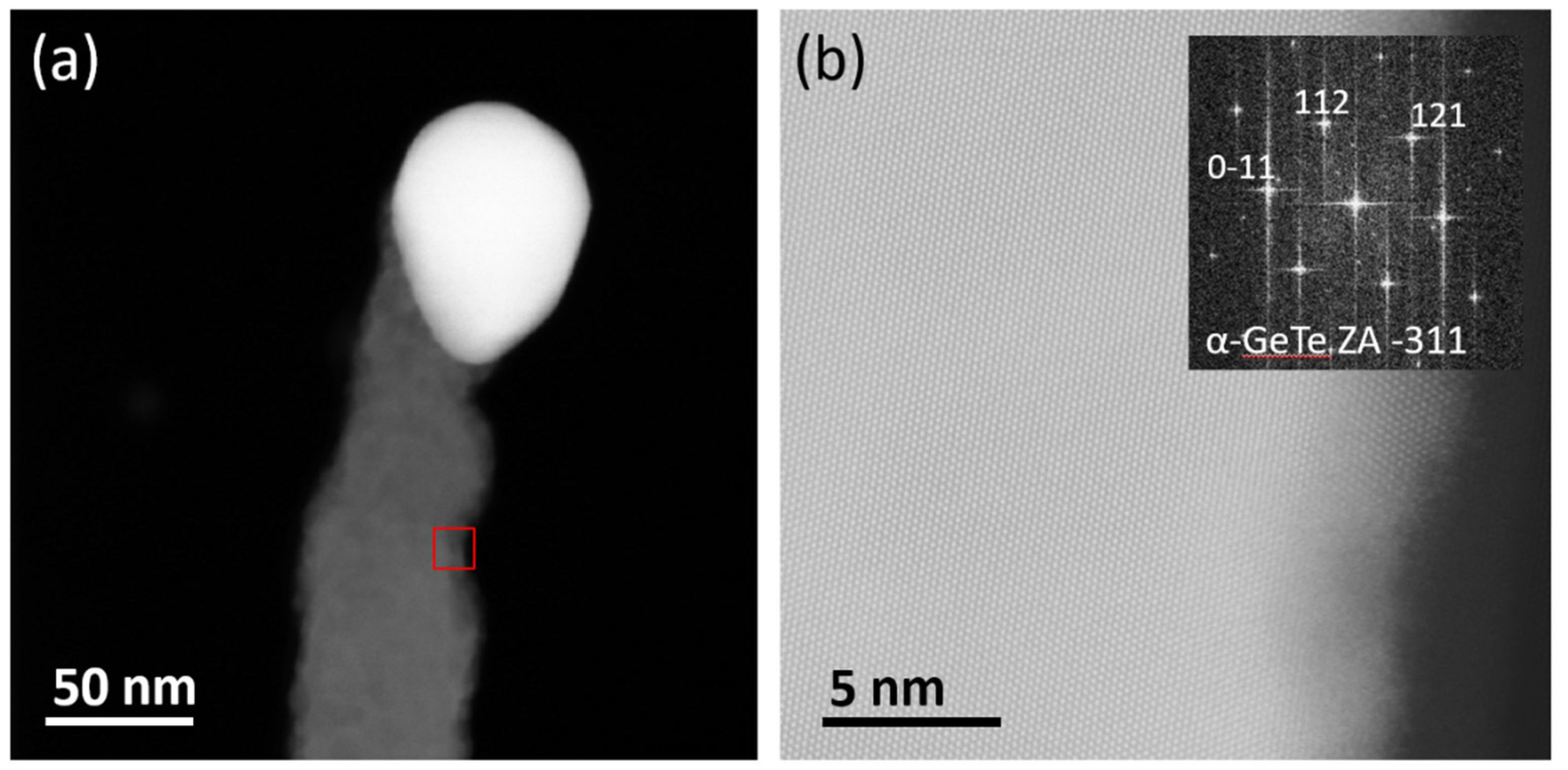
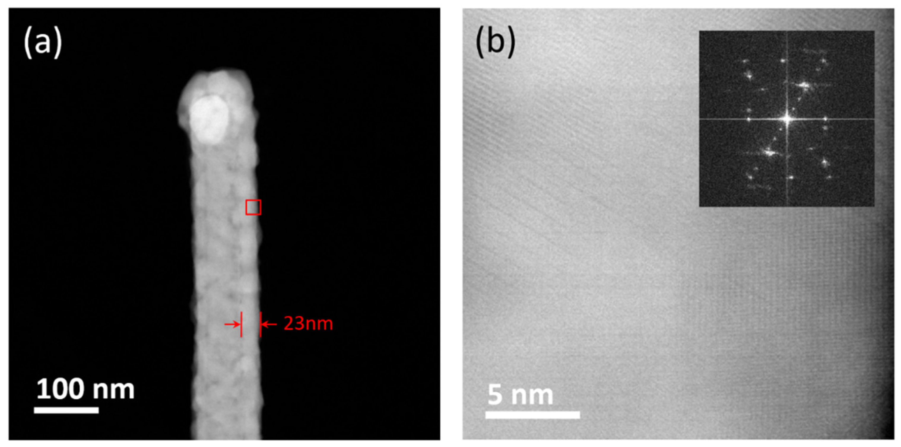
3. Results and Discussion

The first step of our investigation addressed the growth of the GeTe core NWs. Different precursors and different growth parameters were investigated. In particular, using the DSMTe and TDMAGe precursors, we investigated the growth process conditions ranges: T = 380–400 °C, P = 50–300 mbar, with t = 120 min, TDMAGe partial pressure = 4.48 × 10⁻³, and DSMTe partial pressure = 8.06 × 10⁻³. Under non-optimized conditions, only a relatively low fraction of Au NPs gave rise to the VLS process (see Supplementary Material, Figure S1). The best results in terms of morphological characteristics (length and density of NWs) were obtained for T = 400 °C and P = 50 mbar. However, a large density of unreacted Au NPs (see Supplementary Material, Figure S2) was observed. Also, XRD measurements revealed that the NWs were basically formed by Germanium (see Supplementary Material, Figure S3). Replacing the DSMTe precursor with the DiPTe precursor and optimized growth conditions, i.e., T = 400 °C, P = 50 mbar, t = 60 min, DiPTe partial pressure = 8.58 × 10⁻³ mbar, TDMAGe partial pressure = 3.35 × 10⁻³ mbar, the growth of GeTe NWs was achieved (see Figure 1a,b). Au catalyst NPs were observed at the NWs tips, confirming that the growth occurs via the VLS mechanism. Also, SEM observations indicated that the NWs grew with high density and unevenly distributed both on Si (100) and SiO2 substrates, with a certain dispersion in length and diameter (see Supplementary Material, Figures S4 and S5). The density of the NWs increased with increasing the Au NPs sizes. Also, larger NPs produced NWs with larger diameters, consistently with the VLS growth mechanism, and no material growth was found to occur without Au NPs. The effect of the Au NPs size on the diameter of the GeTe NWs is illustrated in Figure S6.
In the second step of the core–shell fabrication, the GeTe NWs were coated with a Sb2Te3 layer using the combination of SbCl3 and DSMTe precursors, under the MOCVD growth conditions: T = room temperature, P = 15 mbar, t = 90 min, SbCl3 partial pressure = 2.23 × 10⁻⁴ mbar, DSMTe partial pressure = 3.25 × 10⁻⁴ mbar, leading to the conformal growth of a uniform and continuous layer on the NWs core (see Figure 1c,d and Supplementary Material Figure S7) [35]. For the shell, it was necessary to lower the deposition temperature down to room temperature to obtain the conformal NWs coating, although with a granular morphology. It was also possible to obtain the Sb2Te3 coating at higher deposition temperatures, but this was detrimental for the conformality, since different voids appeared and the tendency to form crystalline clusters was clearly enhanced. The obtained core–shell NWs have overall diameters in the range of (80–130) nm (see Supplementary Materials Figure S8) and lengths in the range of several microns. The presented results show that, by an appropriate selection of growth conditions, a relatively high density of NWs (i.e., the efficiency of growth catalyzed by Au NPs) and a relatively good control in terms of reproducibility and dispersion of their morphology were achieved.
The results of the large-area XRD analysis on as-grown GeTe core NWs are presented in Figure 2a. The data were analyzed by Rietveld refinement, taking into account not only the peak position, but also the existing background and peak broadening, using the open-source software Maud [36,37,38]. The patterns were simulated using the rhombohedral GeTe structure [39] and cubic Au [40]. The presence of cubic GeTe [41] cannot be excluded. The simulation of the diffracting maxima at a low angle allowed us to extract the lattice parameters of the NWs, which resulted to be a = 8.28 Å and c = 10.55 Å. Moreover, the different intensity of the low-angle diffracting maxima, compared to the powder pattern, suggested that the NWs exhibit a preferential orientation. The data of the GeTe/Sb2Te3 core–shell structures are presented in Figure 2b. Scattering from crystallized Sb2Te3 was evident, as shown by the numerous diffracting maxima assigned to rhombohedral Sb2Te3 [42], with the following lattice parameters, as extracted from Rietveld refinement: a = 4.22Å and c = 30.46Å. The Sb2Te3 crystals also showed a preferential orientation, which was analyzed in more detail by HR-TEM analysis (see in the corresponding section). A shoulder at the right side of the (015) reflection of Sb2Te3, a peak at around 2θ = 29.6°, could be attributed to the (202) main reflection of the GeTe structure, confirming that the core GeTe NWs preserve their crystallinity after the Sb2Te3 deposition.
Micro Raman mapping was performed to analyze the vibrational modes of the deposited GeTe core and GeTe/Sb2Te3 core–shell NWs. Figure 3a shows a large area bright-field optical image of GeTe NWs on the SiO2 substrate with 20 nm Au NPs. The high magnification micrograph revealed that the NWs have a length up to about 5 µm (Figure 3b). The two-dimensional (2D) map in Figure 3c was obtained over the entire region of Figure 3b by measuring a series of Raman spectra with a step-size of 0.5 µm (see the red points indicating the measuring array in Figure 3b). The map’s colour representation refers to a point-by-point correlation with the Raman spectrum, averaged over the full length of the NW, identified on the upper part of the map and reported in Figure 3d. The mean spectrum reveals features similar to those of crystalline GeTe, confirming the well-defined crystalline structure of the NWs. In particular, the peak at about 98 cm−1 assigned to the E mode is specific to the distorted octahedral Ge sites, and it is not present in the spectra of the amorphous material, while the two high-intensity bands at about 126 and 142 cm−1 can be assigned to the A1 mode, attributed to vibrations of Ge atoms in distorted and defective octahedral sites [43,44]. Two more features at 276 and 300 cm−1 could be identified in the spectrum and ascribed to Ge–Ge stretching vibrations, typically observed for Ge nanocrystals [45].
Figure 4 shows the results of Raman mapping on the GeTe/Sb2Te3 core–shell NWs. A single NW was localized and selected by means of optical microscopy in dark-field modality (Figure 4a) and then mapped with a 0.5 µm step-size array of Raman spectra (Figure 4b). Figure 4c reports the spectra corresponding to the Sb2Te3 background (black line, blue area of the map) and the NW (red line, green to red contrast in the map). The background spectrum is characterized by 3 main features at about 69, 112, and 165 cm−1, associated with the A11g (LO), E2g(TO), and A21g(LO) modes of Sb2Te3, respectively [46,47,48]. These peaks are also present in the NW spectrum, together with those already identified for GeTe at 123, 141, and 273 cm−1 (slightly displaced with respect to those of Figure 3d).
The HR-TEM analysis confirmed that the NWs synthesized with Au NPs have a well-defined core–shell structure, where the core is composed of a single crystalline GeTe, surrounded by a polycrystalline Sb2Te3 shell. Figure 5 shows a STEM micrograph of a core GeTe NW with the Au nanoparticle still on the tip. From the high-resolution image of the NW portion, it is revealed that the core GeTe NWs are composed of a single crystalline core, as depicted in Figure 5b. In the inset of Figure 5b, the relative orientations of the Fast-Fourier-Transform (FFT) patterns demonstrate the interplanar distances. By indexing this diffraction pattern, a rhombohedral GeTe phase was recognized, consistent with recent studies of GeTe NWs and the XRD results. EELS confirmed the presence of only Ge and Te along the whole NW, with a ratio compatible with a 1:1 proportion of Ge and Te (see Supplementary Material Figure S9a).
Further, the STEM images of GeTe/Sb2Te3 core–shell NWs showed a uniform and conformal shell around the NWs. Indeed, a clear interface between the core and the shell region is visible on the core–shell NWs (see Figure 6a). This observation indicated the epitaxial growth of the Sb2Te3 layer on top of the GeTe core NW. In Figure 6b, the high-resolution STEM image indicated that the shell is polycrystalline. EELS measurement on the polycrystalline shell confirmed the presence of only Sb and Te, with a ratio compatible with 2:3 of Sb and Te (see Supplementary Material Figure S9b). The GeTe/Sb2Te3 core–shell NWs were found to contain no detectable defects, such as dislocations and stacking faults; the crystal structures of each region of the GeTe/Sb2Te3 core–shell NW heterostructures were in agreement with the XRD results.
The above analyses demonstrated the effectiveness of the present approach in achieving a uniform and conformal deposition of Sb2Te3 at room temperature onto the core GeTe NWs, while maintaining a physically and chemically distinct interface, with minimum interdiffusion of the elements.

4. Conclusions

We presented a bottom-up approach to synthesize core–shell chalcogenide GeTe/Sb2Te3 nanowires, with a diameter down to 80 nm and an average length up to 7 µm. The synthesis of this type of nanoscaled heterostructures could facilitate the understanding of the switching mechanisms in heterostructure-based PCMs and open the way to the realization of advanced microelectronic devices, including multilevel phase-change memories.

Supplementary Materials

The following are available online at https://www.mdpi.com/article/10.3390/coatings11060718/s1, Figure S1: SEM plan view of a sample after MOCVD deposition with TDMAGe and DSMTe precursors at the growth conditions of: TDMAGe partial pressure = 4.48 × 10⁻³ mbar DSMTe partial pressure = 8.06 × 10⁻³ mbar, T = 380 °C, P = 300 mbar, t = 120 min. One visible nanowire generated by the VLS mechanism; plenty of unreacted 20 nm Au particles are also visible. Figure S2: SEM plan view images of nominal GeTe NWs self-assembled by the aid of Au NPs of different size: 10, 20, 30 nm on Si(100) substrates with TDMAGe and DSMTe precursors at the growth conditions of: TDMAGe partial pressure = 4.48 × 10⁻³ mbar DSMTe partial pressure = 8.06 × 10⁻³ mbar, T = 400 °C, P = 50 mbar, t = 120 min. Figure S3: XRD pattern of NWs grown with TDMAGe and DSMTe precursors, signifying only the presence of germanium NWs. Figure S4: SEM images on MOCVD growth of high density GeTe NWs using DiPTe and TDMAGe precursors and 10, 20, 30 and 50 nm Au NPs on (a–d) Si (100), and (e–h) Si/SiO2, respectively; inset: single core GeTe NWs with Au NP on tips. Figure S5: Histograms of the length distribution of the GeTe NWs on Si (100) using DiPTe and TDMAGe precursors with 10, 20, 30 and 50 nm Au NPs, relative to samples of Figure S4 (a–d). Figure S6: Statistical plot of the average diameter distribution of the GeTe core NWs on Si (100) with 10, 20, 30 and 50 nm Au NPs, relative to samples of Figure S4 (a–d). Figure S7: SEM images on MOCVD growth of GeTe/Sb2Te3 core-shell NWs with 10, 20, 30 and 50 nm Au NPs on (a–d) Si (100), and (e–h) Si/SiO2, respectively. Figure S8: Statistical plot of the average diameter distribution of the GeTe/Sb2Te3 core-shell NWs on Si (100) with 10, 20, 30 and 50 nm Au NPs. Figure S9: Electron energy loss spectrum of (a) GeTe core NW and (b) GeTe/Sb2Te3 core-shell NWs.

Author Contributions

Conceptualization, M.L.; investigation, A.K., R.C. (Raimondo Cecchini), C.W., V.M., S.D.S., R.C. (Raffaella Calarco) and M.S.; writing—original draft preparation, A.K., C.W., V.M. and M.S.; writing—review and editing, R.C. (Raimondo Cecchini), S.D.S., R.C. (Raffaella Calarco), G.N. and M.L.; supervision, M.L.; funding acquisition, G.N. and M.L. All authors have read and agreed to the published version of the manuscript.

Funding

This project has received funding from the European Union’s Horizon 2020 research and innovation program under Grant Agreement No. 824957 (“BeforeHand:” Boosting Performance of Phase Change Devices by Hetero- and Nanostructure Material Design). TEM measurements were performed at BeyondNano CNR-IMM, which is supported by the Italian Ministry of Education and Research (MIUR) under project Beyond-Nano (PON a3_00363). The STEM has received funding from the European Union’s Horizon 2020 research and innovation programme under grant agreement No. 823717–ESTEEM3.

Institutional Review Board Statement

Not applicable.

Informed Consent Statement

Not applicable.

Data Availability Statement

Not Applicable.

Conflicts of Interest

The authors declare no conflict of interest.

References

  1. Ovshinsky, S.R. Reversible electrical switching phenomena in disordered structures. Phys. Rev. Lett. 1968, 21, 1450–1453. [Google Scholar] [CrossRef]
  2. Lankhorst, M.H.R.; Ketelaars, B.W.S.M.M.; Wolters, R.A.M. Low-cost and nanoscale non-volatile memory concept for future silicon chips. Nat. Mater. 2005, 4, 347–352. [Google Scholar] [CrossRef] [PubMed]
  3. Long, Y.Z.; Yu, M.; Sun, B.; Gu, C.Z.; Fan, Z. Recent advances in large-scale assembly of semiconducting inorganic nanowires and nanofibers for electronics, sensors and photovoltaics. Chem. Soc. Rev. 2012, 41, 4560–4580. [Google Scholar] [CrossRef]
  4. Zhe, L.; Jing, X.; Di, C.; Guozhen, S. Flexible electronics based on inorganic nanowires. Chem. Soc. Rev. 2014, 44, 161–192. [Google Scholar] [CrossRef]
  5. Yu, R.; Wu, W.; Ding, Y.; Wang, Z.L. GaN nanobelt-based strain-gated piezotronic logic devices and computation. ACS Nano 2013, 7, 6403–6409. [Google Scholar] [CrossRef] [PubMed]
  6. Ng, H.T.; Han, J.; Yamada, T.; Nguyen, P.; Chen, Y.P.; Meyyappan, M. Single crystal nanowire vertical surround-gate field-effect transistor. Nano Lett. 2004, 4, 1247–1252. [Google Scholar] [CrossRef] [Green Version]
  7. Meyyappan, M.; Lee, J.S. The quiet revolution of inorganic nanowires. IEEE Nanotechnol. Mag. 2010, 4, 5–9. [Google Scholar] [CrossRef]
  8. Yu, B.; Sun, X.; Ju, S.; Janes, D.B.; Meyyappan, M. Chalcogenide-nanowire-based phase change memory. IEEE Trans. Nanotechnol. 2008, 7, 496–502. [Google Scholar] [CrossRef]
  9. Eggleton, B.J.; Luther-Davies, B.; Richardson, K. Chalcogenide photonics. Nat. Photonics 2011, 5, 141–148. [Google Scholar] [CrossRef]
  10. Yamada, N.; Ohno, E.; Nishiuchi, K.; Akahira, N.; Takao, M. Rapid-phase transitions of GeTe-Sb2Te3 pseudobinary amorphous thin films for an optical disk memory. J. Appl. Phys. 1991, 69, 2849–2856. [Google Scholar] [CrossRef]
  11. Yamada, N.; Matsunaga, T. Structure of laser-crystallized Ge2Sb2+xTe5 sputtered thin films for use in optical memory. J. Appl. Phys. 2000, 88, 7020–7028. [Google Scholar] [CrossRef]
  12. Longo, M. Advances in nanowire PCM. In Advances in Non-Volatile Memory and Storage Technology; Woodhead Publishing: Amsterdam, The Netherlands, 2019; pp. 443–518. [Google Scholar] [CrossRef]
  13. Lee, S.H.; Ko, D.K.; Jung, Y.; Agarwal, R. Size-dependent phase transition memory switching behavior and low writing currents in GeTe nanowires. Appl. Phys. Lett. 2006, 89, 223116. [Google Scholar] [CrossRef]
  14. Lu, W.; Lieber, C.M. Nanoelectronics from the bottom up. Nat. Mater. 2007, 6, 841–850. [Google Scholar] [CrossRef] [PubMed]
  15. Lee, S.H.; Jung, Y.; Agarwal, R. Highly scalable non-volatile and ultra-low-power phase-change nanowire memory. Nat. Nanotechnol. 2007, 2, 626–630. [Google Scholar] [CrossRef]
  16. Gudiksen, M.S.; Lieber, C.M. Diameter-selective synthesis of semiconductor nanowires. J. Am. Chem. Soc. 2000, 122, 8801–8802. [Google Scholar] [CrossRef]
  17. Yu, D.; Wu, J.; Gu, Q.; Park, H. Germanium telluride nanowires and nanohelices with memory-switching behavior. J. Am. Chem. Soc. 2006, 128, 8148–8149. [Google Scholar] [CrossRef] [PubMed]
  18. Meister, S.; Peng, H.; McIlwrath, K.; Jarausch, K.; Zhang, X.F.; Cui, Y. Synthesis and characterization of phase-change nanowires. Nano Lett. 2006, 6, 1514–1517. [Google Scholar] [CrossRef] [PubMed]
  19. Nukala, P.; Lin, C.C.; Composto, R.; Agarwal, R. Ultralow-power switching via defect engineering in germanium telluride phase-change memory devices. Nat. Commun. 2016, 7, 10482. [Google Scholar] [CrossRef] [Green Version]
  20. Longo, M.; Wiemer, C.; Salicio, O.; Fanciulli, M.; Lazzarini, L.; Rotunno, E. Au-catalyzed self assembly of GeTe nanowires by MOCVD. J. Cryst. Growth 2011, 315, 152–156. [Google Scholar] [CrossRef]
  21. Jung, Y.; Lee, S.H.; Ko, D.K.; Agarwal, R. Synthesis and characterization of Ge2Sb2Te5 nanowires with memory switching effect. J. Am. Chem. Soc. 2006, 128, 14026–14027. [Google Scholar] [CrossRef]
  22. Longo, M.; Stoycheva, T.; Fallica, R.; Wiemer, C.; Lazzarini, L.; Rotunno, E. Au-catalyzed synthesis and characterisation of phase change Ge-doped Sb-Te nanowires by MOCVD. J. Cryst. Growth 2013, 370, 323–327. [Google Scholar] [CrossRef]
  23. Selmo, S.; Cecchini, R.; Cecchi, S.; Wiemer, C.; Fanciulli, M.; Rotunno, E.; Lazzarini, L.; Rigato, M.; Pogany, D.; Lugstein, A.; et al. Low power phase change memory switching of ultra-thin In3Sb1Te2 nanowires. Appl. Phys. Lett. 2016, 109, 213103. [Google Scholar] [CrossRef]
  24. Cecchini, R.; Selmo, S.; Wiemer, C.; Fanciulli, M.; Rotunno, E.; Lazzarini, L.; Rigato, M.; Pogany, D.; Lugstein, A.; Longo, M. In-doped Sb nanowires grown by MOCVD for high speed phase change memories. Micro Nano Eng. 2019, 2, 117–121. [Google Scholar] [CrossRef]
  25. Sun, X.; Yu, B.; Ng, G.; Nguyen, T.D.; Meyyappan, M. III-VI compound semiconductor indium selenide (In2Se3) nanowires: Synthesis and characterization. Appl. Phys. Lett. 2006, 89, 233121. [Google Scholar] [CrossRef]
  26. Gudiksen, M.S.; Lauhon, L.J.; Wang, J.; Smith, D.C.; Lieber, C.M. Growth of nanowire superlattice structures for nanoscale photonics and electronics. Nature 2002, 415, 617–620. [Google Scholar] [CrossRef] [PubMed]
  27. Björ, M.T.; Ohlsson, B.J.; Sass, T.; Persson, A.I.; Thelander, C.; Magnusson, M.H.; Deppert, K.; Wallenberg, L.R.; Samuelson, L. One-dimensional Steeplechase for Electrons Realized. Nano Lett. 2002, 2, 87–89. [Google Scholar] [CrossRef]
  28. Lauhon, L.J.; Gudlksen, M.S.; Wang, D.; Lieber, C.M. Epitaxial core-shell and core-multishell nanowire heterostructures. Nature 2002, 420, 57–61. [Google Scholar] [CrossRef] [PubMed]
  29. Dong, Y.; Yu, G.; McAlpine, M.C.; Lu, W.; Lieber, C.M. Si/a-Si core/shell nanowires as nonvolatile crossbar switches. Nano Lett. 2008, 8, 386–391. [Google Scholar] [CrossRef] [PubMed]
  30. Jung, Y.; Lee, S.H.; Jennings, A.T.; Agarwal, R. Core-shell heterostructured phase change nanowire multistate memory. Nano Lett. 2008, 8, 2056–2062. [Google Scholar] [CrossRef]
  31. Jung, Y.; Ko, D.K.; Agarwal, R. Synthesis and structural characterization of single-crystalline branched nanowire heterostructures. Nano Lett. 2007, 7, 264–268. [Google Scholar] [CrossRef]
  32. Rao, F.; Song, Z.; Zhong, M.; Wu, L.; Feng, G.; Liu, B.; Feng, S.; Chen, B. Multilevel data storage characteristics of phase change memory cell with doublelayer chalcogenide films (Ge2Sb2Te5 and Sb2Te3 ). Jpn. J. Appl. Phys. Part 2 Lett. 2007, 46, L25. [Google Scholar] [CrossRef]
  33. Chong, T.C.; Shi, L.P.; Wei, X.Q.; Zhao, R.; Lee, H.K.; Yang, P.; Du, A.Y. Crystalline amorphous semiconductor superlattice. Phys. Rev. Lett. 2008, 100, 136101. [Google Scholar] [CrossRef] [PubMed]
  34. Wiemer, C.; Ferrari, S.; Fanciulli, M.; Pavia, G.; Lutterotti, L. Combining grazing incidence X-ray diffraction and X-ray reflectivity for the evaluation of the structural evolution of HfO2 thin films with annealing. Thin Solid Films 2004, 450, 134–137. [Google Scholar] [CrossRef]
  35. Cecchini, R.; Mantovan, R.; Wiemer, C.; Nasi, L.; Lazzarini, L.; Longo, M. Weak Antilocalization in Granular Sb2Te3 Thin Films Deposited by MOCVD. Phys. Status Solidi Rapid Res. Lett. 2018, 12, 1800155. [Google Scholar] [CrossRef]
  36. MAUD: Material Analysis Using Diffraction. Available online: http://maud.radiographema.eu/ (accessed on 27 May 2021).
  37. Lutterotti, L.; Chateigner, D.; Ferrari, S.; Ricote, J. Texture, residual stress and structural analysis of thin films using a combined X-ray analysis. Thin Solid Films 2004, 450, 34–41. [Google Scholar] [CrossRef]
  38. Lutterotti, L. Total pattern fitting for the combined size-strain-stress-texture determination in thin film diffraction. Nucl. Instrum. Methods Phys. Res. Sect. B Beam Interact. Mater. Atoms. 2010, 268, 334–340. [Google Scholar] [CrossRef]
  39. Inorganic Crystal Structure Database, ICSD, File n° 56039 for Rhombohedral GeTe; Fiz Karlsruhe: Eggenstein-Leopoldshafen, Germany, 2021.
  40. Inorganic Crystal Structure Database, ICSD, File n° 52700 for Cubic Au; Fiz Karlsruhe: Eggenstein-Leopoldshafen, Germany, 2021.
  41. Inorganic Crystal Structure Database, ICSD, File n° 56037 for Cubic GeTe; Fiz Karlsruhe: Eggenstein-Leopoldshafen, Germany, 2021.
  42. Inorganic Crystal Structure Database, ICSD, File n° 2084 for Rhombohedral Sb2Te3; Fiz Karlsruhe: Eggenstein-Leopoldshafen, Germany, 2021.
  43. Upadhyay, M.; Murugavel, S.; Anbarasu, M.; Ravindran, T.R. Structural study on amorphous and crystalline state of phase change material. J. Appl. Phys. 2011, 110, 083711. [Google Scholar] [CrossRef]
  44. Wang, R.; Campi, D.; Bernasconi, M.; Momand, J.; Kooi, B.J.; Verheijen, M.A.; Wuttig, M.; Calarco, R. Ordered Peierls distortion prevented at growth onset of GeTe ultra-thin films. Sci. Rep. 2016, 6, 32895. [Google Scholar] [CrossRef] [Green Version]
  45. Andrikopoulos, K.S.; Yannopoulos, S.N.; Kolobov, A.V.; Fons, P.; Tominaga, J. Raman scattering study of GeTe and Ge2Sb2Te5 phase-change materials. J. Phys. Chem. Solids 2007, 68, 1074–1078. [Google Scholar] [CrossRef]
  46. Shahil, K.M.F.; Hossain, M.Z.; Goyal, V.; Balandin, A.A. Micro-Raman spectroscopy of mechanically exfoliated few-quintuple layers of Bi2Te3, Bi2Se3, and Sb2Te3 materials. J. Appl. Phys. 2012, 111, 054305. [Google Scholar] [CrossRef] [Green Version]
  47. Sosso, G.C.; Caravati, S.; Bernasconi, M. Vibrational properties of crystalline Sb2Te3 from first principles. J. Phys. Condens. Matter 2009, 21, 095410. [Google Scholar] [CrossRef] [PubMed]
  48. Cecchi, S.; Dragoni, D.; Kriegner, D.; Tisbi, E.; Zallo, E.; Arciprete, F.; Holý, V.; Bernasconi, M.; Calarco, R. Interplay between Structural and Thermoelectric Properties in Epitaxial Sb2+xTe3 Alloys. Adv. Funct. Mater. 2019, 29, 1805184. [Google Scholar] [CrossRef]
Figure 1. SEM images in (a) plan and (b) cross-section view of GeTe NW core, and (c,d) plan view of GeTe/Sb2Te3 core–shell NWs grown on Si (100) with 50 nm Au NPs at different magnifications. The growth durations were 60 and 90 min for the GeTe core and Sb2Te3 shell, respectively.
Coatings 11 00718 g001
Figure 2. XRD patterns and corresponding simulations on (a) GeTe core and (b) GeTe/Sb2Te3 core–shell NWs. The powder patterns of Au [40], GeTe [39], and Sb2Te3 [42] are also added for comparison.
Coatings 11 00718 g002
Figure 3. (a) Large-area optical image of GeTe core NWs on a SiO2 substrate with 20 nm Au NPs; (b) High magnification micrograph localizing single NWs; (c) 2D Raman map acquired on the selected area of (b). The colour representation refers to point-by-point correlation with the Raman spectrum, averaged over the full length of the NW identified on the upper part of the map and reported in (d).
Coatings 11 00718 g003
Figure 4. (a) Image of a GeTe/Sb2Te3 core–shell NW, acquired with the optical microscope in dark field modality; the red points indicate the measuring array used to realize the 2D Raman map in (b). (c) Raman spectra corresponding to the Sb2Te3 background (black line, and blue area of the map) and to the NW (red line, and green to red area in the map).
Coatings 11 00718 g004
Figure 5. (a) STEM micrograph of an individual GeTe core NW; (b) enlarged view at a high resolution of the NW portion indicated by a red square. In the inset, the indexed diffraction pattern is obtained as FFT of the image in (b).
Coatings 11 00718 g005
Figure 6. (a) STEM micrograph of a GeTe/Sb2Te3 core–shell NW; (b) enlarged view at a high resolution of the shell (red square) and the corresponding FFT in the inset, showing its polycrystalline nature.
Coatings 11 00718 g006
Publisher’s Note: MDPI stays neutral with regard to jurisdictional claims in published maps and institutional affiliations.

