Article

Synthesis and Properties of p-Si/n-Cd1−xAgxO Heterostructure for Transparent Photodiode Devices

by
Mannarsamy Anitha
1,
Karuppiah Deva Arun Kumar
2,
Paolo Mele
2,*,
Nagarajan Anitha
3,
Karunamoorthy Saravanakumar
4,
Mahmoud Ahmed Sayed
5,6,
Atif Mossad Ali
5,6 and
Lourdusamy Amalraj
7
1
Department of Physics, Sri Vidhya College of Arts and Science, Virudhunagar 626005, India
2
Shibaura Institute of Technology, College of Engineering, Saitama 337-8570, Japan
3
Department of Physics, Devanga Arts College, Arupukottai 626101, India
4
Department of Chemistry, VHNSN College, Virudhunagar Tamilnadu 626001, India
5
Department of Physics, Faculty of Science, King Khalid University, Abha 61413, Saudi Arabia
6
Physics Department, Faculty of Science, Al-Azher University, Assiut 71524, Egypt
7
Department of Physics, VHNSN College, Virudhunagar 626001, India
*
Author to whom correspondence should be addressed.
Coatings 2021, 11(4), 425; https://doi.org/10.3390/coatings11040425
Submission received: 7 March 2021 / Revised: 1 April 2021 / Accepted: 2 April 2021 / Published: 7 April 2021

Abstract

:
We developed silver-doped Cd1xAgxO thin films (where x = 0, 0.01, 0.02, 0.03 and 0.04) on amorphous glass substrate by an automated nebulizer spray pyrolysis set-up. The XRD patterns show rock salt cubic crystal structures, and the crystallite sizes vary with respect to Ag doping concentrations. SEM images exhibited a uniform distribution of grains with the addition of Ag; this feature could support the enhancement of electron mobility. The transmittance spectra reveal that all films show high transmittance in the visible region with the observed bandgap of about 2.40 eV. The room temperature photoluminescence (PL) studies show the increase of near-band-edge (NBE) emission of the films prepared by different Ag doping levels, resulting in respective decreases in the bandgaps. The photodiode performance was analyzed for the fabricated p-Si/n-Cd1xAgxO devices. The responsivity, external quantum efficiency and detectivity of the prepared p-Si/n-Cd1xAgxO device were investigated. The repeatability of the optimum (3 at.% Ag) photodiode was also studied. The present investigation suggests that Cd1xAgxO thin films are the potential candidates for various industrial and photodetector applications.

1. Introduction

Thin film technology is a quick-moving field which includes the application of structures, film processing and the manufacture of devices by controlling the shape and size of grains at the nanometer range [1]. Nanometer-range thin films have distinctive and specific physical properties associated with their size [2]. Metal oxide semiconductors have attracted increasing attention because of their wide range of applications in various devices, which include optical communications, photodiode, gas sensors, low emissive windows and solar cells [3]. In the last decade, researchers developed metal oxide-based transparent detectors such as gas sensors and photodetectors [4]. At present, photodetectors are widely studied for use in imaging scanners, switching, touch panels and light sensors. Zheng et al. [4] studied the flexible ZnO–CdO nanofiber arrays for UV photodetectors with 95% transparency. Metal oxides are very common and easily available on Earth, and they are used to fabricate transparent devices due to their low absorption in the visible region. The typical wide bandgap metal oxides such as SnO2, ZnO, TiO2 and In2O3 can perform as ultraviolet light sensors [5]. The visible range-absorbing CdO is commonly used to fabricate solar cell devices, and it also might be a potential candidate to detect the light spectrum [5].
CdO is an n-type semiconductor with a direct optical bandgap of 2.3–2.5 eV [6] and nonstoichiometric composition, owing to the defects of oxygen vacancies or cadmium interstitials that act as double-loaded donors [7,8]. The unique qualities of CdO metal oxide are its low cost, chemical stability and wide availability.
In general, different kinds of nanostructures offer more attractive properties due to their high surface-to-volume ratios, consequently enhancing the light-sensing ability. The different nanostructures can be grown by changing several parameters, such as the chemical synthesis process, rate of the growth time, substrate temperature, nature of the substrate, and doping. However, metal doping can effectively modify the nature of grains in the host lattice; consequently, it could affect the surface-to-volume ratio or the observing capability of light on the host film surface, whereas the doping can enhance the grain growth level and Debye length, resulting in improved optoelectrical properties. Moreover, doping is a key parameter to improve the performance of any semiconducting materials and used in wide range of device applications [9]. Previously, CdO systems were prepared with different doping elements such as aluminum [10], manganese [11], gallium [12], indium [13], zinc [14] and silver [15] for various applications. However, the silver (Ag) metal element has been commonly used because of its numerous good characteristics and its notable chemical reactivity in solutions [16]. Ag is one of the active metals that might be easily oxidized by the doping process. Therefore, it is very interesting to understand the role of silver in a transparent CdO matrix. Recently, scientists worked on pure and Ag-doped CdO nanostructures through various techniques [15,17,18,19]. To our knowledge, the silver-doped CdO thin film prepared by nebulizer spray pyrolysis has not been reported. Kumar et al. [20,21] reported the advantages of the nebulizer spray pyrolysis (NSP) technique. The main advantages of the NSP technique are good adherence, mechanical stability, being inexpensive, fine droplet formation and capability for mass production for large area deposition that are required for industrial device applications.
Therefore, the aim of the present study is to fabricate Cd1–xAgxO thin films (where x = 0, 0.01, 0.02, 0.03 and 0.04) via an automated nebulizer spray pyrolysis method. Ag doping induced the improvement of the optical and electrical properties for the performance of solar cells and other optical devices. Recently, Kathalingam et al. [22] reported the fabrication of an n-Sn:CdO/p-Si heterostructure for visible photodetectors. They suggested that a high-bandgap n-type semiconductor can be easily coated on p-Si substrates to fabricate heterojunction solar cells. In addition, the fabricated p-Si/n-CdO heterojunction could decrease the recombination loss due to a mixture of small-bandgap absorber material and high-bandgap window material. Based on the above work, we report the development of the n-Ag:CdO/p-Si heterostructure and study the photoresponse. This work is propounded for the first time and suggests that the CdO thin films could be utilized for the development of multilayer photodetectors.

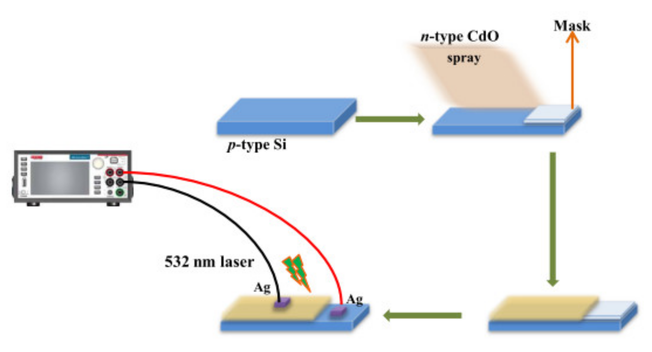
2. Materials and Methods

Ag-doped CdO films were prepared on glass substrates using the automated nebulizer spray pyrolysis technique. A total of 0.1 M of high-purity (3N) cadmium acetate dehydrate (Cd(CH3(COO)2)·2H2O) was liquefied by using a mixture of isopropyl alcohol and deionized water, with a volume ratio of 1:3 (20 mL). Silver nitrate (AgNO3) was used as a dopant precursor with different concentrations, as given in Supplementary Table S1. The prepared precursor solution was sprayed onto the heated glass substrates with a surface area of 25 mm2. The heated substrates were maintained at a constant temperature of 200 °C +/− 2 °C using a PID (select 500) controller. The parameters were maintained during spray deposition, including a carrier gas (compressed air) pressure of 14.7 × 10⁴ Nm−2, a distance between the nozzle and substrate of 10 mm and a solution flow rate of 0.5 mL/min, which were previously optimized. When the sprayed solution fell on the heated substrates, thermal decomposition took place on the film surface, resulting in yellow-colored CdO particles being grown. The structural properties of films were analyzed by an X`PERT-PRO diffractometer (Malvern Pananalytical Ltf, Malvern, UK) (λ = 0.15406 nm) with CuKα radiation. The SEM investigation was performed by a scanning electron microscope (TESCAN VEGA-III, Tescan, Brno, Czech Republic). The elemental analysis was carried out using energy dispersive X-ray spectroscopy (EDX). The optical properties of the films were characterized by a UV-visible spectrophotometer (Shimadzu-UV 1800 model, Shimadzu, Kyoto, Japan). The reflectance spectrum of the samples was recorded by a UV-2400 PC Series. The photoluminescence (PL) spectra was recorded using a fluorescence spectrophotometer (HITACHI F-7000), Hitachi, Tokyo, Japan with an excitation wavelength of ~325 nm. A 532 nm laser wavelength was used as illumination light to measure the photosensitivity, external quantum efficiency (EQE) and detectivity values with the help of a Keithley source meter (model 2450, Tectronix Inc, Beaverton, OR, USA).

3. Results and Discussion

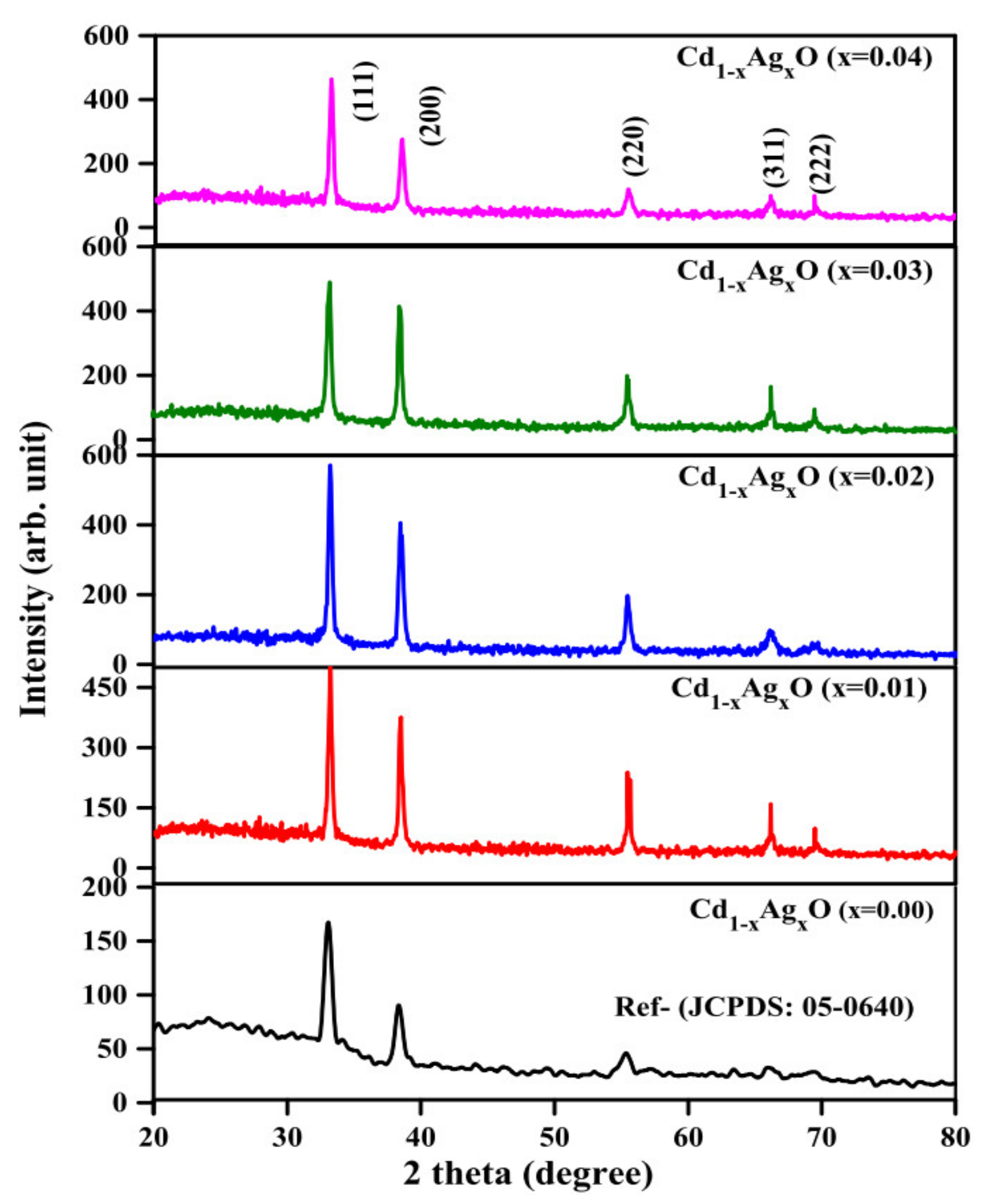
3.1. Structural Analysis

The phase structure of the Ag-doped Cd1xAgxO films (where x = 0, 0.01, 0.02, 0.03 and 0.04) was studied by XRD, which is shown in Figure 1. The identified diffraction peaks 2θ(111) = 33.03°, 2θ(200) = 38.44°, 2θ(220) = 55.34°, 2θ(311) = 66.03° and 2θ(222) = 69.35° matched well with the cubic structure of CdO (space group: Fm3m) (JCPDS Card No. 05-0640).
In Figure 1, a highly intense peak obtained at 2θ = 33.03° for all CdO films indicates a preferential growth orientation along the (111) direction. After the inclusion of Ag, the intensity of the XRD characteristic peaks increased gradually up to the optimum doping level (Ag = 0.03), due to Cd2+ ions being replaced by Ag+ ions because of the larger ionic radius of Ag+ (0.126 nm) compared with Cd2+ (0.095 nm). The increase in peak intensity or decrease of the full width at half maximum (β) indicated the enhancement of film crystallinity and grain sizes [23]. The comparative cure for 2 at.% and 3 at.% Ag-doped CdO films are given in Figure S1. The figure confirms that the (111) plane increased with the increasing Ag doping level. However, by increasing the Ag doping beyond the optimum level (Ag = 0.03), the peak intensity and film crystallinity started to decrease (Ag = 0.04). This may be attributed to the higher solution quantity or Ag precipitation, resulting a powder-like film being formed on the film surface. In addition, the peak reduction may have possibly occurred by the slight variation of both the Cd and Ag ionic radii, which led to the creation of lattice distortion or crystal imperfections [24]. It is worth noting that there were no impurity phase formations related to Ag or Ag3O4, even for a higher dopant level up to 4%. Rex et al. [24] reported the same trend in Ag-doped PbS (4% Ag) films under the NSP method. This could justify that the doping of Ag effectively substituted the site of Cd, resulting the formation of single-phase CdO. As expected, there was no observable peak shift in the predominant (111) plane, confirming the structural purity of CdO.
The lattice parameters were calculated using the standard relation of the cubic structure [25]. The calculated values increased with respect to the increase in Ag concentration up to 3% Ag and then reduced for higher doping levels, and they are tabulated in Table 1.
This behavior could be due to the change in the concentration of the native defects or structural defects developed in the prepared host films. The structural parameters, such as the crystallite size (D) and strain (ε), were determined using standard relations [26,27]. The calculated D and ε values of the Cd1–xAgxO films with respect to different Ag concentrations are given in Table 1. The crystallite size enhanced with the increase in Ag content, and then it slightly reduced for higher Ag (4 at.%) doping levels. This could possibly vary with the change of structural defects like ε. The defect factors of ε decreased initially as a function of the increasing Ag up to 3% and then slightly increased for the 4% Ag-doped CdO thin film. A decrease in defect values could be attributed to the enhancement of crystallinity caused by the periodic arrangement of atoms in the host crystal structure.
The texture coefficient TC(hkl) values demonstrate the crystal orientation of the (111) plane of the prepared Cd1–xAgxO system by using X-ray data with the equation given below [26]:
TC ( hkl ) = I ( hkl ) / I 0 ( hkl ) N r 1 I ( hkl ) / I 0 ( hkl )
where I(hkl), I0(hkl) and N denote the usual meanings. From Table 1, it is found that the calculated TC values increased with the increasing Ag doping concentration and then finally decreased. The obtained TCs for all the films were higher than 1 (TC > 1), which indicates the preferable grain growth in certain orientations. This result suggests that a lot of crystallites were gathered along the (111) plane, which helped improve the electrical performance. The variation of TC values was the same as in our previous report [26]. The XRD studies showed that the Ag, up to 3 at.%, maintained good structural quality (crystallinity) with minimum defects (strain) compared with that of other prepared films.

3.2. Surface Morphology Analysis

The observed SEM images of the pure CdO and Cd1–xAgxO films are shown in Figure S2. The pure CdO film showed densely packed, brain-like grains [28] uniformly distributed on the entire film surface, whereas the bunch of irregular spherical grains without the presence of voids were observed in 1–2 at.% Ag-doped films. The film with 3 at.% Ag doping exhibited spherical shaped grains with well-defined grain boundaries [29]. The particles were further agglomerated by increasing the doping beyond the optimum level (4 at.% Ag). Moreover, the grain sizes increased by increasing the doping concentrations up to 3 at.%. Thereafter, the grain size slightly decreased for higher-level doping (4 at.% Ag). Thus, various levels of Ag doping concentrations effectively modified the host CdO film surface, and this observation could be correlated with the XRD results. The change in grain size signified the change of grain boundaries in the host lattice. The composition of the pure and Ag-doped CdO (3 at.%) films were confirmed by energy dispersive X-ray spectroscopy (EDX). The obtained EDX spectra of the prepared films are shown in the inset of Figure S2. The expected elements of Cd, O and Ag are present with the desired atomic percentages which were taken. The composition percentages of Cd, O, and Ag were 48.07%, 49.06%, and 2.87%, respectively, for 3 at.% Ag.

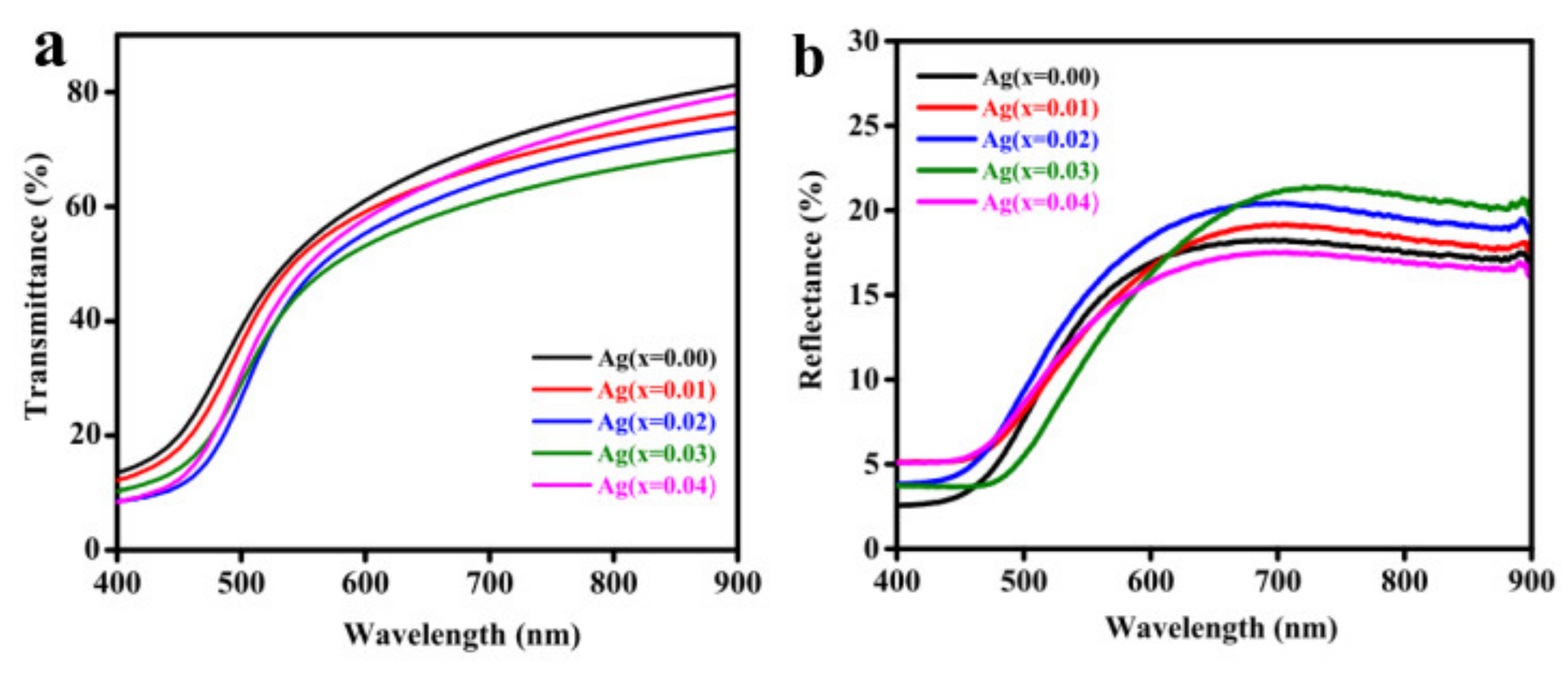
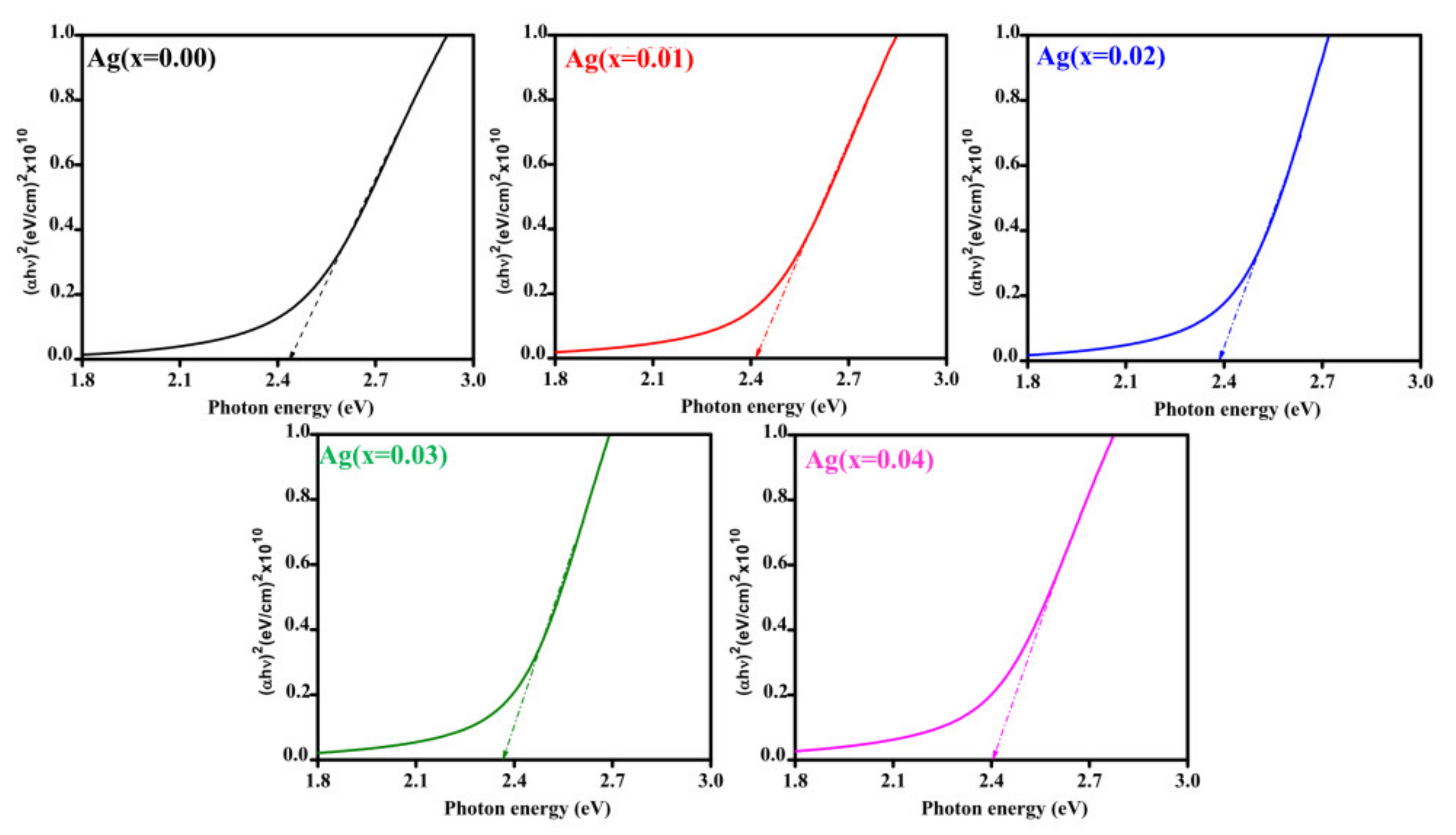
3.3. Optical Analysis

The optical properties were explored with a UV-visible spectrophotometer. The optical transmittance and reflectance spectra of Cd1–xAgxO films are given in Figure 2a,b, respectively. From Figure 2a, the obtained transparency was ~70% in the visible wavelength range. Transmittance was reduced slightly with the increasing doping concentration, which may have been due to the decrement in oxygen vacancies. Furthermore, the lessening of transmittance was due to the change in grain size and film thickness [30]. The observed transmittance range confirmed that the prepared film could work as a transparent photodetector.
The transmittance value was not as close to the lower wavelength of the visible region due to the appearance of absorption. Furthermore, the primary absorption edge was shifted in the direction of the higher wavelength (redshift) with respect to the Ag concentration. This edge in the wavelength can decide the variation of the bandgap because the transmittance is associated with stimulating the charge carriers from the valence to conduction bands. The optical bandgap is related by the following equation [24]:
α h ν = B ( h ν   - E g ) n  
where B is a constant and Eg is the bandgap of the material. The direct bandgaps of the Cd1xAgxO films were obtained from a plot of (αhν)2 versus , as illustrated in Figure 3. The bandgap values of the prepared films are given in Table 2. The Eg value of the pure CdO was 2.45 eV, which matched well with the one reported by Usharani et al. [31], whereas the Eg values for the doped CdO films were found to decrease from 2.43 eV to 2.37 eV with the increase in the Ag doping level. This might be due to the substitution of Ag in the sites of Cd. A similar reduction in the bandgap was observed for the Ag-doped PbS film under the NSP method [24]. Moreover, redshift absorption (toward a higher wavelength) further confirmed the decrease of the bandgap. For a higher doping concentration (4 at.% Ag), the bandgap was slightly enhanced due to the doped Ag ions effectively modifying the band structure of the host CdO lattice. The reduction of film crystallinity (XRD) and blueshift of the near-band-edge (NBE) emission (PL) occurred from 3 at.% to 4 at.% Ag-doped CdO, as evidenced by the increase of the bandgap. As shown in Table 2, the bandgap was low for the film doped with 3 at.% Ag, which absorbed more visible light than the other films. Consequently, the photoelectric interaction was enhanced, resulting in improving the photosensor performance with respect to the applied voltage.
Other optical factors, such as the refractive index (n) and reflectance (R), play an important role for any optical device. The R and n values of the Cd1xAgxO thin films are listed in Table 2. The R values of the Ag-doped CdO thin films increased from 17% to 22% as a function of the doping concentration increasing from 1 at.% to 3 at.% Ag. The variation of reflectance was in oppositional behavior to the transmittance with respect to the doping concentration, as shown in Figure 2b. The refractive index n was determined from the values of reflectance and the extinction coefficient (k) using the following equation [32]:.
n = ( 1 + R ) ( 1 R ) + 4 R ( 1 R ) 2 k 2
From Table 2, the observed low value of n confirmed the smooth surface morphologies and minimum reflectance of the prepared films. The variation of n systematically increased with the increasing Ag doping level due to the decrease of transmittance (T). Commonly, the n variation had the opposite trend of T, which may be attributed to the increase of light scattering of the photons. The estimated n values were in the range of 2.36–2.62 in the visible range for different doping concentration, as shown in Table 2.

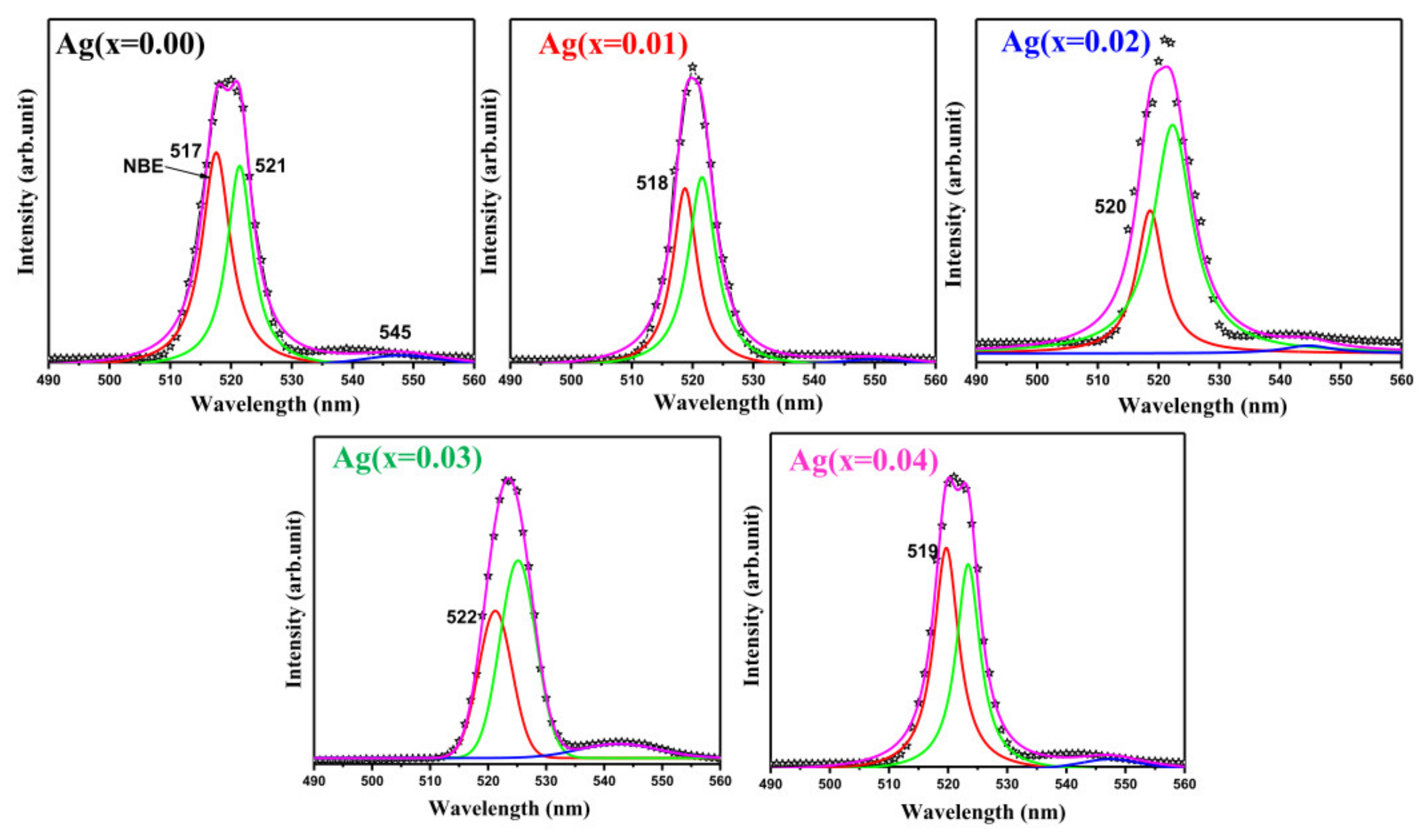
3.4. Photoluminescence Analysis

Photoluminescence (PL) was used to investigate the factor of the electron hole pairs in the semiconductor materials [33].
Figure 4 presents the photoluminescence spectra of the prepared Cd1xAgxO films obtained by an excitation wavelength of ~325 nm. The room temperature PL spectra mainly consisted of one strong green emission band observed at ~520 nm (2.38 eV) in all the prepared films. The green emission was consistent with the near-band-edge emission (NBE), which originated from the recombination of the electron and holes. In addition, the observed NBE emission by PL correlated well with the bandgap obtained by the UV-visible study. Similar green emission was previously observed by Velusamy et al. [23] for CdO films. The overall peak intensity increased as a function of the Ag doping concentration. This might be representative of the increasing quantity of Ag ions on the host CdO lattice and the decrease in space between the Ag+ and Cd2+ ions, while for the higher doping level, the peak intensity decreased slightly, which may have been due to the increasing interstitial placement level of the Ag ions near the Cd sites. The NBE emission shifted gradually toward longer wavelength sides (from 517 to 522 nm) with increasing Ag doping levels. Consequently, there was a decrease in the energy gap, as evidenced from Figure 3. Gaussian curve fitting was used to find the additional defect peaks from the prepared Cd1–xAgxO films. From the fitted PL cure, a peak was observed at 521 nm for all the prepared films. This might have been the presence of Cd as interstitials or native state defects. As seen from the figure, the defect peaks were considerably increased with respect to the Ag doping concentration, and as a result, it could help to enhance the photoelectric performance. In addition, the other low-intensity green emission peak was identified at ~545 nm for all the films, which arose due to the presence of defects like oxygen vacancies, as is clearly shown in Figure 4. The film with 3 at.% Ag doping had more oxygen vacancy at the film surface than the others. Therefore, it could react well with the photon from the laser light. Moreover, the Ag doping induced a redshift, which may have been due to the surface area [34], resulting in a reduction of the bandgap. We believe that the Ag dopant can enhance the surface area and crystalline quality. The above factors might be evidence for enhancing light absorption and improving charge carrier generation. A similar result was observed for Nd-doped ZnO thin films by Paul et al. [35].

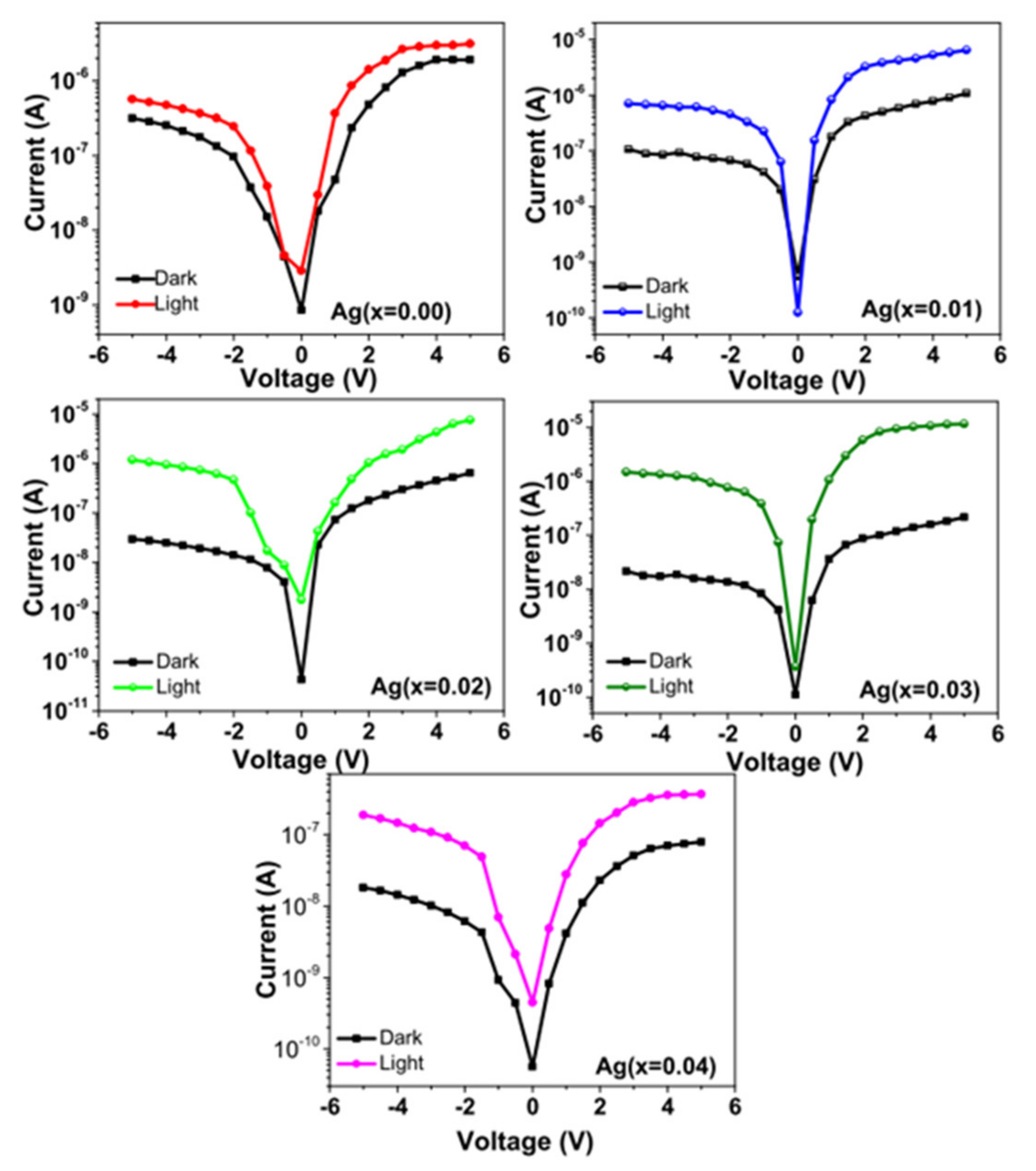
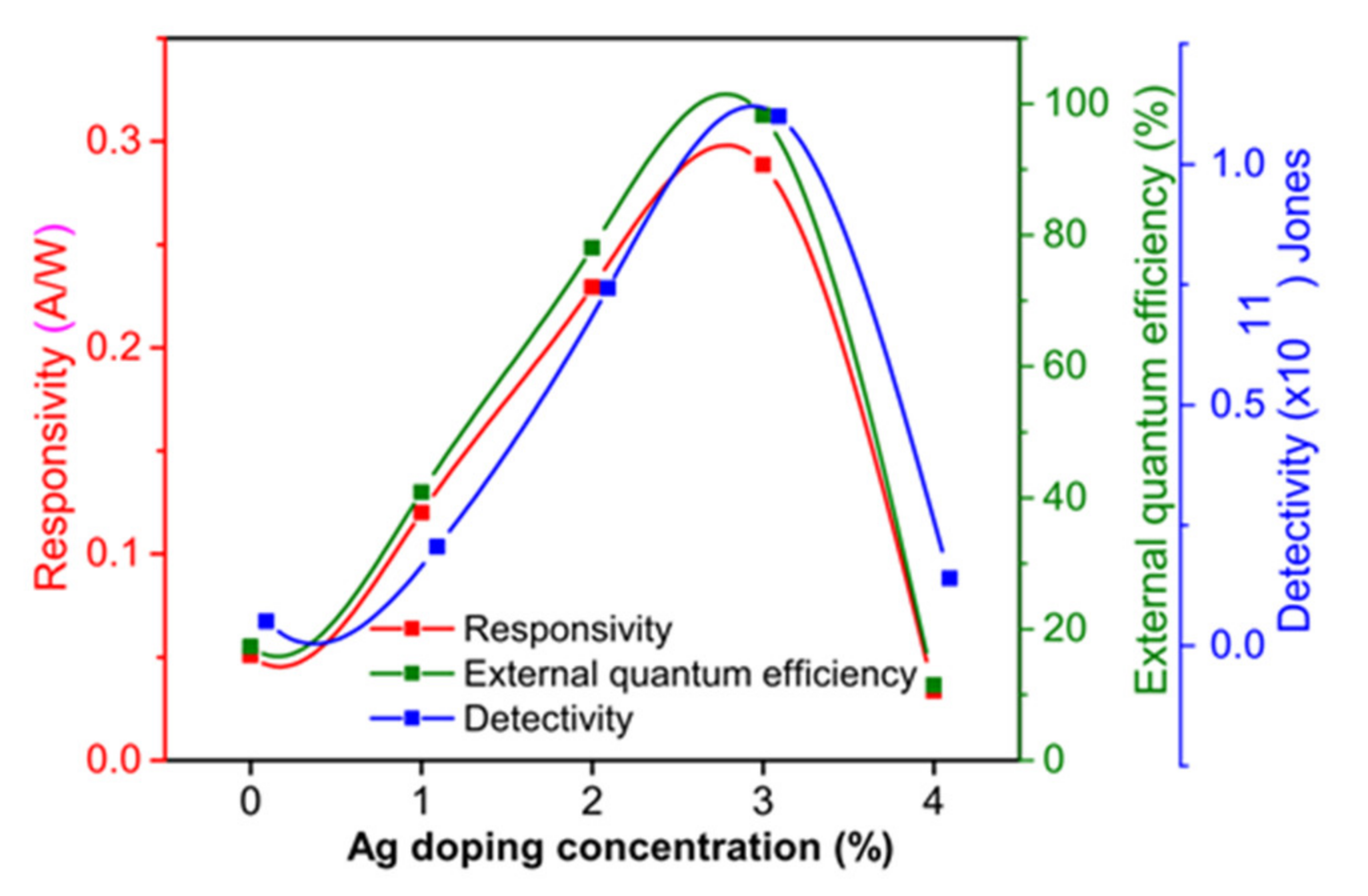
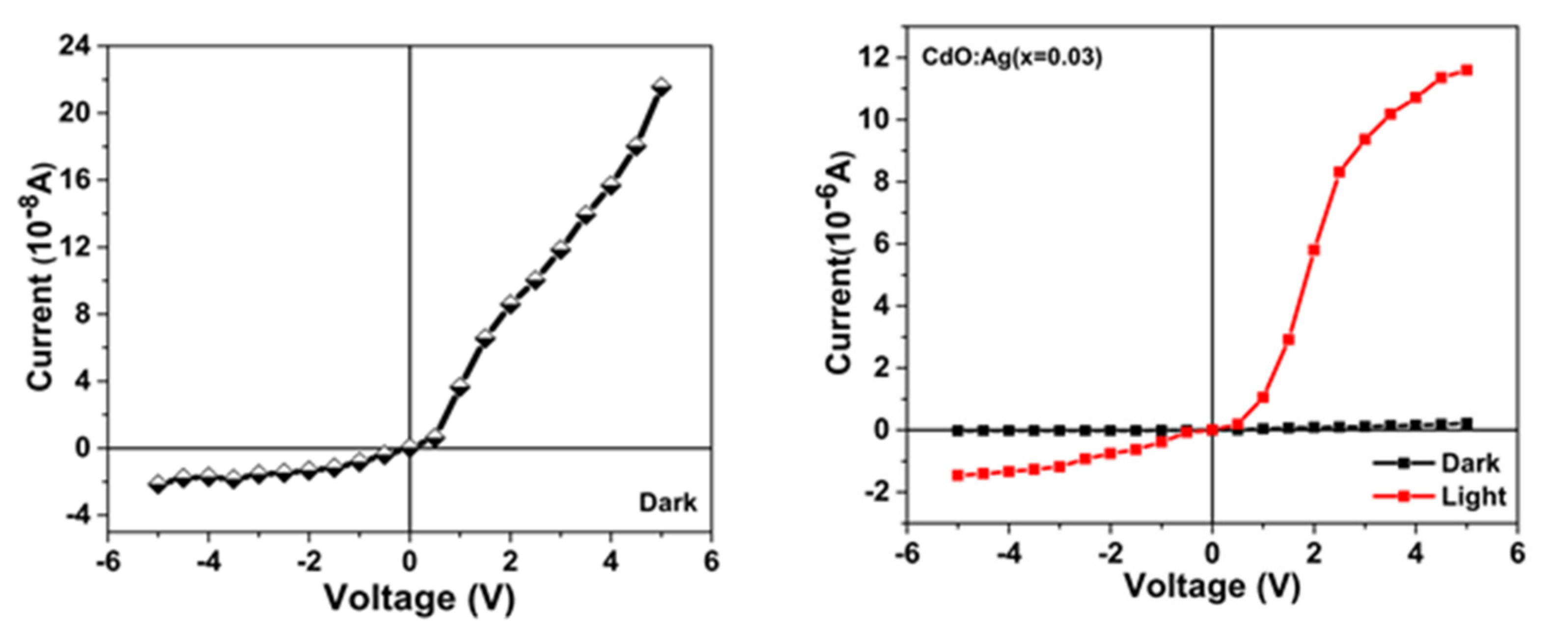
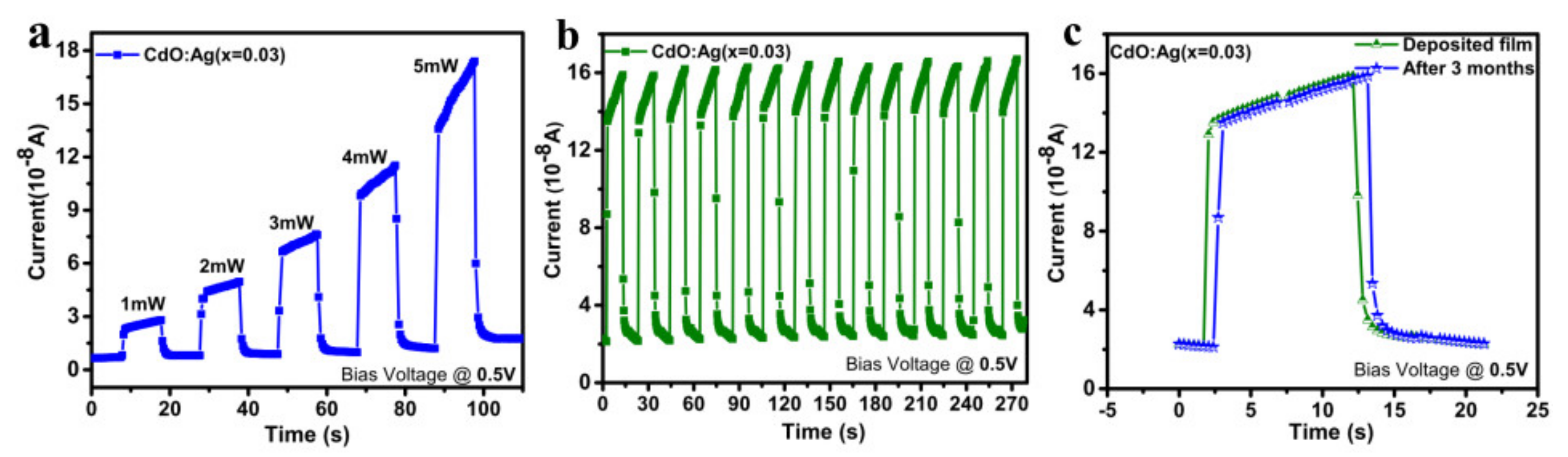
3.5. Photodiode Preparation and Properties

The schematic diagram of the fabricated heterojunction photodiode p-Si/n-Cd1xAgxO/Ag structure is shown in Figure 5. Before fabricating the heterostructure device, the native oxide should be removed from the Si substrate. Here, we used HF:H2O (1:10) solution treatment and then rinsed it with deionized water. The Ag-doped CdO films were coated on the p-type silica substrate by the NSP method to form a heterojunction device. Silver paste was used as contact electrodes on both the p-Si and n-CdO surfaces to measure the photocurrent with respect to the bias voltage.
The photocurrent performance of the prepared photodiodes was measured using a ~532 nm laser with a Keithley source meter (model-2450) at room temperature. The current–voltage (I–V) characteristics were investigated at different bias voltages from −5 V to +5 V under dark and UV illumination conditions. The measured I–V spectra of the p-Si/n-Cd1–xAgxO/Ag structure are given in Figure 6. The observed dark and light currents both increased gradually with respect to the increase in applied voltage. However, the current level was higher for light illumination compared to the dark condition, due to the increase of electrons when the diode interacted with the incident photons obtained from light. The photocurrent (under light) was enhanced significantly for both the forward and reverse biases, indicating successful light sensing for the fabricated photodiodes. It was observed that the photocurrent was nearly two orders of magnitude higher than the dark current, likely due to the inner photoelectric effect (i.e., when a photon of sufficient energy falls on the photodiode, it creates an electron hole pair).
The external quantum efficiency (EQE), responsivity (R*) and specific detectivity (D*) values were calculated using the standard relations, which were E Q E = R h c e λ , R * = I P A × P i n and D * = R A 2 e I d [35,36]. The calculated D* and EQE values were directly proportional to R, which increased for the Ag-doped CdO photodiodes, as shown in Figure 7.
The prepared photodiode responsivity increased from 0.05 AW−1 to 0.28 AW−1 for the pure CdO to 3 at.% Ag-doped CdO photodiode and then decreased to 0.03 AW−1 for the higher doping of Ag (4 at.%). The maximum external quantum efficiency was ~98.21%, observed for the optimum CdO photodiode (3 at.% Ag-doped CdO) when compared with others. Ravikumar et al. [37] obtained an EQE value of 73.03% for a 5% Nd-doped CdO, which was a bit lower than our value. The specific detectivity was enhanced gradually from 5.07 × 10⁹ to 1.10 × 10¹¹ (jones) for the pure to 3 at.% Ag-doped CdO photodiode. This observed specific detectivity was comparably higher than the previously reported one for CdS:Ag/Si [38]. The observed good photoelectric properties may have been due to maximum electron hole pair generation when it interacted with high-energy photons.
The linear dynamic range (LDR) is one of the important factors to recognize the performance of any photodiode and photodetectors, and it can be estimated using the following equation [39]:
L D R = 20 log I min I max
where Imin and Imax represent the dark current and light current, respectively. The observed LDR of the prepared p-Si/n-Cd1xAgxO/Ag structure was 36.7 dB for the 3 at.% Ag-doped CdO. This value was close to the ZnO-based p-n junction diode [39], though it is worth noting that the CdO-based visible photodiode prepared by a simple spray method showed a reasonable LDR value compared with that of the other p-n junction [39,40]. Hence, we believe that this is an essential move to fabricate the flexible photodiodes.
To find the ideality factor, the I–V characteristics of the optimum p-Si/n-CdO:Ag photodiode (3 at.% Ag) under dark and light conditions are given in Figure 8. The observed photocurrent exponentially increased when compared with the dark current. In this work, the observed photocurrent level (11.6 × 10⁻⁶ A at 5V) was higher than the previously reported values. Recently, Xiao et al. [41] fabricated the Ga2O3:CdO-based amorphous thin-film transistor and observed a photocurrent of about 20 nA at 20 V.
The ideality factor (η) is one of the important parameters for any heterostructure diode for finding the recombination mechanisms ruling inside the diode. Based on the theory of thermionic emission (TE), the ideality factor (η) can be calculated with the use of dark IV curves by the following relation [42]:
I = I 0 exp e V η k T 1
where e is the electron charge, V is the voltage, I0 is the saturation current, k is the Boltzmann constant and T is the absolute temperature (300 K). The η value of the diode was calculated from the slope of the linear part at the forward bias curves, and the value was 3.2. For an ideal diode, the η is equal to one, which means that the current flow is due to thermionic emission, though the reported value is commonly higher than unity. In our case, the ideality factor value was found to be higher than unity, indicating the existence of interface states or surface defects on the native oxide layer. This can possibly happen from thermionic emission and other electron transport mechanisms. Tunneling recombination in particular could play a leading role in controlling the junction behavior and increasing the η [43]. Yakuphanoglu et al. [44] observed an ideality factor of 5.41 for a nanocluster-based n-CdO/p-Si photodiode.
In order to understand the photosensing performance of the optimal photodiode (3 at.% Ag-doped CdO), the photocurrent experiment was performed under different light intensities from 1 mW/cm2 to 5 mW/cm2 at 0.5 V, as shown in Figure 9a. When the diode interacted with different intensities of light (turning on the light), the current quickly reached a specific level, and when the light was turned off, the photocurrent reached its beginning stage. This was because of the increase of the number of photo-generated charge carriers and the free electrons that supported the increase in the current for the light-on condition, whereas the numbers of free electrons went down when the light was off [45]. The photocurrent varied between the light-on and off conditions due to the trapping of deep levels of charge carriers [46]. The figure shows that the current values were increasing gradually with the increasing intensities of light from 1 mW/cm2 to 5 mW/cm2. The time taken for increasing and decreasing the current level was measured from the fabricated p-Si/n-CdO:Ag structure. The increase in time was considered to be ~90% of the time taken to reach the maximum value, and the reverse was the decrease in time. The increase in time (τinc) and decrease in time (τdec) were 0.8 s and 1.0 s, respectively.
To understand the photodetection capability (repeatability) of the prepared heterostructure, a constant laser power (5 mW/cm2) was used as a function of the increasing time. Figure 9b shows the transient photocurrent response of the prepared heterostructure under a bias voltage of 0.5 V. The transient photosensing performances maintained the same range with respect to the increase in time, which confirmed good sensing capability and repeatability. Figure 9c illustrates the variation of the current for fresh and 3 months-aged p-Si/n-CdO:Ag photodiodes to define the stability of the optimum sensor. It was found that the electrical current range reached above 95% of the fresh photodiode at 0.5 V, while the response time was a bit slower (1.2 s) when compared with the fresh photodiode (0.8 s). At the same time, the recovery time was nearly equal (~1.0 s) for both the fresh and aged photodiodes. Hence, we conclude that the aged photodiode still showed good photosensing performance and good stability (reproducibility) even after 3 months.

4. Conclusions

In summary, the successful preparation of transparent Cd1xAgxO thin films on glass and p-Si substrates for photodiode investigation. The XRD pattern revealed the formation of a cubic structured CdO lattice with a (111) preferential orientation, and there were no peak shifts in all the films, which confirmed the absence of an impurity phase. The SEM images revealed that all the films had spherical grains, and the grain size increased with the increase in the Ag doping level. EDX analysis revealed that the Cd, O and Ag elements were present in the prepared films. The undoped film showed the maximum transmittance of ~75%, and the corresponding bandgap was 2.45 eV, which confirmed the transparent nature of the CdO material. The obtained bandgap decreased with an increase in the doping level. From the present study, it is evident that the fabricated p-Si/n-CdO:Ag photodiode showed an improved photoresponse in the visible region.

Supplementary Materials

Attached The following are available online at https://www.mdpi.com/article/10.3390/coatings11040425/s1, Figure S1: The comparative cure for 2 at.% and 3 at.% of Ag doped CdO thin films, Figure S2. The scanning electron micrographs for the prepared CdO thin films with EDX spectrum for pure and 3 at.% Ag. Table S1: Preparation of Ag doping concentrations for CdO thin films (0.1 M).

Author Contributions

Conceptualization, methodology, data analysis and writing—original draft, M.A.; project supervision, writing and approval for submission of the manuscript, L.A.; interpretation of data, writing—review and editing, K.D.A.K. and P.M.; interpretation of data—review and editing, N.A. and K.S.; discussion and reviewing of the manuscript, M.A.S. and A.M.A. All authors have read and agreed to the published version of the manuscript.

Funding

The authors from KKU extended their appreciation to the Deanship of Scientific Research at King Khalid University for funding this work through the research group program under grant number R.G.P.1/298/42.

Institutional Review Board Statement

Not applicable.

Informed Consent Statement

Not applicable.

Data Availability Statement

Data are contained within the article.

Conflicts of Interest

The authors declare no conflict of interest.

References

  1. Lopez-Serrano, A.; Muñoz-Olivas, R.; Sanz-Landaluze, J.; Olasagasti, M.; Rainieri, S.; Camara, C. Comparison of bioconcentration of ionic silver and silver nanoparticles in zebrafish eleutheroembryos. Environ. Pollut. 2014, 191, 207–214. [Google Scholar] [CrossRef] [PubMed]
  2. Auffan, M.; Rose, J.; Bottero, J.-Y.; Lowry, G.V.; Jolivet, J.-P.; Wiesner, M.R. Towards a definition of isnorganic nanoparticles from an environmental, health and safety perspective. Nat. Nanotechnol. 2009, 4, 634–641. [Google Scholar] [CrossRef] [PubMed]
  3. Sivakumar, S.; Venkatesan, A.; Soundhirarajan, P.; Khatiwada, C.P. Synthesis, characterizations and anti-bacterial activities of pure and Ag doped CdO nanoparticles by chemical precipitation method. Spectrochim. Acta Part A Mol. Biomol. Spectrosc. 2015, 136, 1751–1759. [Google Scholar] [CrossRef]
  4. Zheng, Z.; Gan, L.; Li, H.; Ma, Y.; Bando, Y.; Golberg, D.; Zhai, T. A Fully Transparent and Flexible Ultraviolet–Visible Photodetector Based on Controlled Electrospun ZnO-CdO Heterojunction Nanofiber Arrays. Adv. Funct. Mater 2015, 25, 5885–5894. [Google Scholar] [CrossRef]
  5. Rajput, J.K.; Pathak, T.K.; Swart, H.C.; Purohit, L.P. Synthesis of CdO Nanoflowers by Sol-Gel Method on Different Substrates with Photodetection Application. Phys. Status Solidi 2019, 216, 1900093. [Google Scholar] [CrossRef]
  6. Chopra, S.R. Thin Film Solar Cells; Plenum Press: New York, NY, USA, 1993. [Google Scholar]
  7. Minami, T.; Ida, S.; Miyata, T. High rate deposition of transparent conducting oxide thin films by vacuum arc plasma evaporation. Thin Solid Film. 2002, 416, 92–96. [Google Scholar] [CrossRef]
  8. Pan, L.L.; Li, G.Y.; Lian, J.S. Structural, optical and electrical properties of cerium and gadolinium doped CdO thin films. Appl. Surf. Sci. 2013, 274, 365–370. [Google Scholar] [CrossRef]
  9. Aydın, C.; El-Nasser, H.M.; Yakuphanoglu, F.; Yahia, I.S.; Aksoy, M. Nanopowder synthesis of aluminum doped cadmium oxide via sol–gel calcination processing. J. Alloy Compd. 2011, 509, 854–858. [Google Scholar] [CrossRef] [Green Version]
  10. Wongcharoen, N.; Gaewdang, T.; Wongcharoen, T. Electrical Properties of Al-Doped CdO Thin Films Prepared by Thermal Evaporation in Vacuum. Energy Procedia 2012, 15, 361–370. [Google Scholar] [CrossRef] [Green Version]
  11. Gao, W.; Yang, S.; Yang, S.; Lv, L.; Du, Y. Synthesis and magnetic properties of Mn doped CuO nanowires. Phys. Lett. A 2010, 375, 180–182. [Google Scholar] [CrossRef]
  12. Thambidurai, M.; Muthukumarasamy, N.; Ranjitha, A.; Velauthapillai, D. Structural and optical properties of Ga-doped CdO nanocrystalline thin films. Superlattices Microstruct. 2015, 86, 559–563. [Google Scholar] [CrossRef]
  13. Zheng, B.; Hu, W. Influence of substrate temperature on the structural and properties of In-doped CdO films prepared by PLD. J. Semicond. 2013, 34, 053003. [Google Scholar] [CrossRef]
  14. Ravichandran, A.T.; Robert Xavier, A.; Pushpanathan, K.; Nagabhushana, B.M.; Chandramohan, R. Structural and optical properties of Zn doped CdO nanoparticles synthesized by chemical precipitation method. J. Mater. Sci. Mater. Electron. 2016, 27, 2693–2700. [Google Scholar] [CrossRef]
  15. Yüksel, M.; Şahin, B.; Bayansal, F. Nano structured CdO films grown by the SILAR method: Influence of silver-doping on the morphological, structural and optical properties. Ceram. Int. 2016, 42, 6010–6014. [Google Scholar] [CrossRef]
  16. Malachová, K.; Praus, P.; Rybková, Z.; Kozák, O. Antibacterial and antifungal activities of silver, copper and zinc montmorillonites. Appl. Clay Sci. 2011, 53, 642–645. [Google Scholar] [CrossRef]
  17. Salem, A. Silver-doped cadmium oxide nanoparticles: Synthesis, structural and optical properties. Eur. Phys. J. Plus 2014, 129, 263. [Google Scholar] [CrossRef]
  18. Majid, A.; Afzal, Z.; Murtaza, S.; Nabi, G.; Ahmad, N. Synthesis and Characterization of Silver Doped Cadmium Oxide Nanoparticles. J. Adv. Phys. 2013, 2, 116–118. [Google Scholar] [CrossRef]
  19. Saravanakumar, K.; Muthuraj, V.; Jeyaraj, M. The design of novel visible light driven Ag/CdO as smart nanocomposite for photodegradation of different dye contaminants. Spectrochim. Acta Part A Mol. Biomol. Spectrosc. 2018, 188, 291–300. [Google Scholar] [CrossRef]
  20. Deva Arun Kumar, K.; Mele, P.; Ponraj, J.S.; Haunsbhavi, K.; Varadharajaperumal, S.; Alagarasan, D.; Algarni, H.; Angadi, B.; Murahari, P.; Ramesh, K. Methanol solvent effect on photosensing performance of AZO thin films grown by nebulizer spray pyrolysis. Semicond. Sci. Technol. 2020, 35, 085013. [Google Scholar] [CrossRef]
  21. Deva Arun Kumar, K.; Valanarasu, S.; Tamilnayagam, V.; Amalraj, L. Structural, morphological and optical properties of SnS2 thin films by nebulized spray pyrolysis technique. J. Mater. Sci. Mater. Electron. 2017, 28, 14209–14216. [Google Scholar] [CrossRef]
  22. Kathalingam, A.; Kesavan, K.; Rana, A.U.H.S.; Jeon, J.; Kim, H.-S. Analysis of Sn Concentration Effect on Morphological, Optical, Electrical and Photonic Properties of Spray-Coated Sn-Doped CdO Thin Films. Coatings 2018, 8, 167. [Google Scholar] [CrossRef] [Green Version]
  23. Velusamy, P.; Babu, R.R.; Ramamurthi, K.; Dahlem, M.S.; Elangovan, E. Highly transparent conducting cerium incorporated CdO thin films deposited by a spray pyrolytic technique. RSC Adv. 2015, 5, 102741–102749. [Google Scholar] [CrossRef]
  24. Rosario, S.R.; Kulandaisamy, I.; Kumar, K.D.A.; Ramesh, K.; Ibrahium, H.A.; Awwad, N.S. Ag-doped PbS thin films by nebulizer spray pyrolysis for solar cells. Int. J. Energy Res. 2020, 44, 4505–4515. [Google Scholar] [CrossRef]
  25. Velusamy, P.; Babu, R.R.; Ramamurthi, K.; Elangovan, E.; Viegas, J.; Dahlem, M.S.; Arivanandhan, M. Characterization of spray pyrolytically deposited high mobility praseodymium doped CdO thin films. Ceram. Int. 2016, 42, 12675–12685. [Google Scholar] [CrossRef]
  26. Anitha, M.; Saravanakumar, K.; Anitha, N.; Amalraj, L. Influence of a novel co-doping (Zn + F) on the physical properties of nano structured (1 1 1) oriented CdO thin films applicable for window layer of solar cell. Appl. Surf. Sci. 2018, 443, 55–67. [Google Scholar] [CrossRef]
  27. Haunsbhavi, K.; Deva Arun Kumar, K.; Mele, P.; Aldossary, O.M.; Ubaidullah, M.; Mahesh, H.M.; Murahari, P.; Angadi, B. Pseudo n-type behaviour of nickel oxide thin film at room temperature towards ammonia sensing. Ceram. Int. 2021. [Google Scholar] [CrossRef]
  28. Bagheri Khatibani, A.; Hallaj, Z.A.; Rozati, S.M. Some physical properties of CdO:F thin films prepared by spray pyrolysis. Eur. Phys. J. Plus 2015, 130, 254. [Google Scholar] [CrossRef]
  29. Thirumoorthi, M.; Prakash, J.T.J. A study of Tin doping effects on physical properties of CdO thin films prepared by sol–gel spin coating method. J. Asian Ceram. Soc. 2016, 4, 39–45. [Google Scholar] [CrossRef] [Green Version]
  30. Dakhel, A.A. Correlated transport and optical phenomena in Ga-doped CdO films. Sol. Energy 2008, 82, 513–519. [Google Scholar] [CrossRef]
  31. Usharani, K.; Balu, A.R.; Nagarethinam, V.S.; Suganya, M. Characteristic analysis on the physical properties of nanostructured Mg-doped CdO thin films—Doping concentration effect. Prog. Nat. Sci. Mater. Int. 2015, 25, 251–257. [Google Scholar] [CrossRef] [Green Version]
  32. Anand, V.; Sakthivelu, A.; Karuppiah, D.A.K.; Valanarasu, S.; Ganesh, V.; Shkir, M.; AlFaify, S.; Algarni, H. Rare earth Eu3+ co-doped AZO thin films prepared by nebulizer spray pyrolysis technique for optoelectronics. J. Sol-Gel Sci. Technol. 2018, 86, 293–304. [Google Scholar] [CrossRef]
  33. Balachandran, S.; Praveen, S.G.; Velmurugan, R.; Swaminathan, M. Facile fabrication of highly efficient, reusable heterostructured Ag–ZnO–CdO and its twin applications of dye degradation under natural sunlight and self-cleaning. RSC Adv. 2014, 4, 4353–4362. [Google Scholar] [CrossRef]
  34. Farhat, O.F.; Halim, M.M.; Ahmed, N.M.; Qaeed, M.A. ZnO nanofiber (NFs) growth from ZnO nanowires (NWs) by controlling growth temperature on flexible Teflon substrate by CBD technique for UV photodetector, Superlattice. Microst 2016, 100, 1120. [Google Scholar] [CrossRef]
  35. Poul Raj, I.L.; Valanarasu, S.; Hariprasad, K.; Ponraj, J.S.; Chidhambaram, N.; Ganesh, V.; Ali, H.E.; Khairy, Y. Enhancement of optoelectronic parameters of Nd-doped ZnO nanowires for photodetector applications. Opt. Mater. 2020, 109, 110396. [Google Scholar] [CrossRef]
  36. Shkir, M.; Ashraf, I.M.; Khan, A.; Khan, M.T.; El-Toni, A.M.; AlFaify, S. A facile spray pyrolysis fabrication of Sm:CdS thin films for high-performance photodetector applications. Sens. Actuators A Phys. 2020, 306, 111952. [Google Scholar] [CrossRef]
  37. Ravikumar, M.; Chandramohan, R.; Kumar, K.D.A.; Valanarasu, S.; Ganesh, V.; Shkir, M.; Alfaify, S.; Kathalingam, A. Effect of Nd doping on structural and opto-electronic properties of CdO thin films fabricated by a perfume atomizer spray method. Bull. Mater. Sci. 2019, 42, 8. [Google Scholar] [CrossRef] [Green Version]
  38. Najm, N.I.; Hassun, H.K.; al-Maiyaly, B.K.H.; Hussein, B.H.; Shaban, A.H. Highly selective CdS:Ag heterojunction for photodetector applications. Aip Conf. Proc. 2019, 2123, 020031. [Google Scholar] [CrossRef]
  39. Hanna, B.; Surendran, K.P.; Narayanan Unni, K.N. Low temperature-processed ZnO thin films for p–n junction-based visible-blind ultraviolet photodetectors. RSC Adv. 2018, 8, 37365–37374. [Google Scholar] [CrossRef] [Green Version]
  40. Gong, X.; Tong, M.; Xia, Y.; Cai, W.; Moon, J.S.; Cao, Y.; Yu, G.; Shieh, C.-L.; Nilsson, B.; Heeger, A.J. High-Detectivity Polymer Photodetectors with Spectral Response from 300 nm to 1450 nm. Science 2009, 325, 1665–1667. [Google Scholar] [CrossRef]
  41. Xiao, X.; Liang, L.; Pei, Y.; Yu, J.; Duan, H.; Chang, T.-C.; Cao, H. Solution-processed amorphous Ga2O3:CdO TFT-type deep-UV photodetectors. Appl. Phys. Lett 2020, 116, 192102. [Google Scholar] [CrossRef]
  42. Rhoderick, E.H.; Williams, R.H. Metal-Semiconductor Contacts; Clarendon Press Oxford: Oxford, UK, 1978. [Google Scholar]
  43. Moun, M.; Kumar, M.; Garg, M.; Pathak, R.; Singh, R. Understanding of MoS(2)/GaN Heterojunction Diode and its Photodetection Properties. Sci. Rep. 2018, 8, 11799. [Google Scholar] [CrossRef] [PubMed]
  44. Yakuphanoglu, F.; Caglar, M.; Caglar, Y.; Ilican, S. Electrical characterization of nanocluster n-CdO/p-Si heterojunction diode. J. Alloy. Compd. 2010, 506, 188–193. [Google Scholar] [CrossRef]
  45. Gozeh, B.A.; Karabulut, A.; Yildiz, A.; Dere, A.; Arif, B.; Yakuphanoglu, F. SILAR Controlled CdS Nanoparticles Sensitized CdO Diode Based Photodetectors. Silicon 2020, 12, 1673–1681. [Google Scholar] [CrossRef]
  46. Çiçek, O.; Tecimer, H.U.; Tan, S.O.; Tecimer, H.; Altındal, Ş.; Uslu, İ. Evaluation of electrical and photovoltaic behaviours as comparative of Au/n-GaAs (MS) diodes with and without pure and graphene (Gr)-doped polyvinyl alcohol (PVA) interfacial layer under dark and illuminated conditions. Compos. Part B Eng. 2016, 98, 260–268. [Google Scholar] [CrossRef]
Figure 1. XRD patterns of Ag-doped CdO thin films with different Ag doping levels.
Coatings 11 00425 g001
Figure 2. (a) Transmittance and (b) reflectance spectra of pure and Ag-doped CdO thin films.
Coatings 11 00425 g002
Figure 3. Optical bandgap spectra of pure and Ag-doped CdO thin films.
Coatings 11 00425 g003
Figure 4. Gaussian curve-fitted photoluminescence spectra of pure and Ag-doped CdO thin films.
Coatings 11 00425 g004
Figure 5. The schematic diagram of the prepared p-Si/n-CdO:Ag structure.
Coatings 11 00425 g005
Figure 6. Light and dark current–voltage (I–V) characteristics of the fabricated the p-Si/n-Cd1–xAgxO/Ag structures.
Coatings 11 00425 g006
Figure 7. The variations of the responsivity (R), specific detectivity (D*) and external quantum efficiency (EQE) with respect to different Ag doping amounts.
Coatings 11 00425 g007
Figure 8. I_V characteristics of the fabricated p-Si/n-CdO:Ag photodiode measured in dark and illuminated conditions at a bias voltage between –5 and +5 V.
Coatings 11 00425 g008
Figure 9. (a) Photocurrent kinetics with respect to different light intensities from 1 mW/cm2 to 5 mW/cm2. (b) Repeatability and (c) stability at 5 mW/cm2 for the optimum 3 at.% Ag-doped CdO photodiode.
Coatings 11 00425 g009
Table 1. Structural properties of Cd1_xAgxO thin films.
Ag Doping Level (at.%)Crystallite Size
(nm)
Strain
ε
Lattice
Constant a = b = c (Å)
Unit Cell
Volume (v) (Å)3
TC
0280.00424.6828102.691.76
1290.00404.6842102.781.93
2310.00384.6854102.862.18
3340.00344.6869102.972.35
4320.00384.6893103.111.97
Table 2. Optical properties of Cd1–xAgxO thin films.
Ag Doping Level (at.%)For λ = Average of 600–900 nmBandgap Eg (eV)
T%R%n
075172.412.45
171192.532.43
268202.582.40
365222.622.37
470162.362.41
Publisher’s Note: MDPI stays neutral with regard to jurisdictional claims in published maps and institutional affiliations.

