Article

Growth of GaP Layers on Si Substrates in a Standard MOVPE Reactor for Multijunction Solar Cells

1
Instituto de Energía Solar, Universidad Politécnica de Madrid, Av. Complutense 30, 28040 Madrid, Spain
2
IM2NP, Aix-Marseille Université, 13397 Marseille, France
3
Departamento de Física, Universidad Carlos III de Madrid, Av. Universidad 30, Leganés, 28911 Madrid, Spain
*
Authors to whom correspondence should be addressed.
Coatings 2021, 11(4), 398; https://doi.org/10.3390/coatings11040398
Submission received: 25 February 2021 / Revised: 22 March 2021 / Accepted: 25 March 2021 / Published: 30 March 2021

Abstract

:
Gallium phosphide (GaP) is an ideal candidate to implement a III-V nucleation layer on a silicon substrate. The optimization of this nucleation has been pursued for decades, since it can form a virtual substrate to grow monolithically III-V devices. In this work we present a GaP nucleation approach using a standard MOVPE reactor with regular precursors. This design simplifies the epitaxial growth in comparison to other routines reported, making the manufacturing process converge to an industrial scale. In short, our approach intends to mimic what is done to grow multijunction solar cells on Ge by MOVPE, namely, to develop a growth process that uses a single reactor to manufacture the complete III-V structure, at common MOVPE process temperatures, using conventional precursors. Here, we present the different steps in such GaP nucleation routine, which include the substrate preparation, the nucleation itself and the creation of a p-n junction for a Si bottom cell. The morphological and structural measurements have been made with AFM, SEM, TEM and Raman spectroscopy. These results show a promising surface for subsequent III-V growth with limited roughness and high crystallographic quality. For its part, the electrical characterization reveals that the routine has also formed a p-n junction that can serve as bottom subcell for the multijunction solar cell.

1. Introduction

Silicon technology dominates the terrestrial solar energy market [1], but it presents an important issue–further device development is practically at a standstill since they have virtually reached their theoretical efficiency limit (26.7% [2] versus 29.6% of the theoretical maximum [3]). On the other hand, multijunction solar cells based on III-V semiconductors are the most efficient solar cell technology—the world record is currently 47.1% [4]—but they are too expensive for terrestrial applications due to the raw materials involved and production costs. In view of this situation, in the search for photovoltaic progress, alternative new generations of solar cells have awakened great interest. Such is the case of the conjugation of III-V multijunction solar cells on silicon substrates. These architectures can combine the high efficiency of multijunction solar cells with the low-cost advantages of large area silicon substrates [5,6,7]. Despite its great promise, this integration is not direct and must tackle key difficulties, such as the large difference in thermal expansion coefficients and their significant lattice mismatch.
The nucleation of III-V semiconductors on silicon substrates for photovoltaic applications has been the goal of many research works since the 1980s [6]. Among the great palette of III-V compounds, gallium phosphide (GaP), with a lattice parameter which differs only in 0.37% [8,9] from that of silicon at room temperature (approximately 5.45 Å in GaP vs. 5.43 Å in Si) stands out. Accordingly, this mismatch is the smallest that can be found between any III-V semiconductor and silicon, minimizing the chances for defect generation in a monolithically-grown structure. For this reason, GaP is an ideal candidate for a III-V nucleation layer on Si, because a defect-free growth at this stage is instrumental. For example, the interface between the III-V semiconductor and the underlying Si determines the quality of the subsequent layers, since many defects—most commonly threading dislocations or antiphase domains—can propagate upwards, impacting the electronic quality of the layers which will be used for devices [10]. As shown in Figure 1, in our target application (a multijunction solar cell), a GaAsP top cell will be grown on the GaP/Si virtual substrate. To this end, a transparent metamorphic GaAsyP1−y buffer on the GaP layer is needed to accommodate the lattice mismatch between the Si bottom cell and the GaAsP top cell. The GaP also acts as a window layer to passivate the n-type emitter of the Si bottom cell due to its high bandgap (2.26 eV) and the favorable offsets of the valence and conduction bands [11,12]. This tandem GaAsP/Si solar cell, shown in Figure 1, could reach theoretical efficiencies of 41.9% [13].
The epitaxial growth by MOVPE of the structure in Figure 1 entails a number of challenges, being the nucleation of a defect-free GaP layer on the silicon wafer a crucial stepping stone. In this sense, the seminal work by Volz and co-workers [10] describes a consolidated and reproducible MOVPE growth routine for the achievement of high-quality, planar and smooth GaP layers grown on Si, that has been successfully replicated by some other groups around the world [14] and has been used in the most successful implementations of the solar cell in Figure 1 [15]. This routine starts with a high temperature annealing of the Si wafer—above 900 °C—under H2 to pyrolyze the native SiO2 layer. Then the double-stepped pristine silicon surface, necessary to avoid antiphase domains [16], is achieved through a Si homoepitaxial growth, which entails the use of a specific reactor with two chambers in order to avoid cross-contamination. Initially, the GaP/Si nucleation —including the Si homoepitaxy—takes place in one chamber and then the sample needs to be transferred to a different chamber (or even to another reactor) to proceed with the subsequent growth of the III-V active layers of the device, which, in the case of multijunction cells, typically include a variety of III-As and III-P compounds, as schematically shown in Figure 1. On the one hand, this transfer guarantees that the active layers do not suffer from Si background contamination and, on the other hand, the nucleation chamber remains free of any arsenic [17]. Furthermore, the GaP is grown using pulsed growth at low temperatures [10], which demands the use of specific group-V precursors (i.e., TBP) in addition to PH3, used in the rest of the III-V structure, and thus impacts on process costs.
In this study we present a simpler routine for the growth of GaP layers on Si, that could be implemented in any standard MOVPE reactor, used to grow III-As and III-P compounds, without the need of multiple chambers, Si homoepitaxial growth or extra precursors. Therefore, the novelty of this work is to develop a routine that could be implemented in any industrial reactor currently used to grow commercial multijunction solar cells on germanium. In our case, the nucleation routine is carried out in a single-run –both nucleation and device layers– and in a single MOVPE reactor. This process mimics what is done for GaInP/Ga(In)As/Ge triple-junction solar cells grown on a Ge wafer, where the nucleation and active layers are grown in a single run, using standard precursors, while also creating the Ge bottom cell in the wafer during the first steps of the growth.
With this target in mind, in this work we present such a GaP on Si MOVPE nucleation routine, which consists of: (1) a thermal annealing step for deoxidation and contaminant removal; (2) an AsH3 pre-exposure, which serves as a cleaning aide and to improve the superficial wetting; and (3) the growth of the GaP layer proper. The GaP layers grown are characterized from the structural and morphological points of view and the diffusion of n-dopants into the silicon substrate for the formation of the Si bottom subcell is assessed too.

2. Materials and Methods

2.1. Experimental

The wafers used for these experiments were Si (100) misoriented 4° towards [111] with a resistivity of 5–10 Ω·cm. Prior to their loading into the reactor, the wafers were chemically cleaned by an HF-dip with HF–H2O (1:6) for 3 min and rinsed in deionized water and blown dry with N2, afterwards. All the samples reported in this research have been grown in a commercial AIX200/4 MOVPE reactor (Aixtron, Herzogenrath, Germany) using PH3 and TMGa as precursors for the GaP growth, AsH3 for the pre-exposures and, in some processes, DETe for n-type doping the GaP layer. The reactor chamber has been kept “coated” in all the epitaxies –i.e., all reactor quartzware and the vacuum system have not been cleaned between runs–, and thus with the usual background of As, Ga and P from previous runs. In-situ reflectance anisotropy spectroscopy (RAS) measurements have been carried out during the routines with a EpiRAS tool (LayTec, Berlin, Germany). The process temperature has been measured using a pyrometer, namely, a Laytec EpiTT. It should be noted that all temperature values given in the following sections correspond to actual pyrometer readings and not to heater set points.
The morphology and roughness assessment has been carried out using atomic force microscopy (AFM), being the tool employed a multimode Nanoscope III A (Bruker, Billerica, MA, USA) in tapping mode. Raman spectra and cross-section transmission electron microscopy (TEM) images have been taken to evaluate the quality of the layers and to detect if impurities or other compounds are present in the crystal. Raman microprobe measurements were made using a HR800-UV spectrometer (Horiba-Jobin Yvon, Longjumeau, France) coupled with a metallographic microscope (Olympus, Tokyo, Japan). The spectra measured were obtained using as excitation the red line of an He–Ne laser (λ = 632.8 nm). High resolution TEM (HRTEM) images were acquired with a Tecnai F20 system (Philips, Eindhoven, Netherlands) operated at 200 keV. Electrochemical CV profiling, using a CPV21 tool (WEP, Furtwangen, Germany) was used to measure free carrier concentration to quantify the diffusion of n-type dopant elements into the Si substrate in order to verify the creation of a p-n junction and thus a silicon bottom cell.

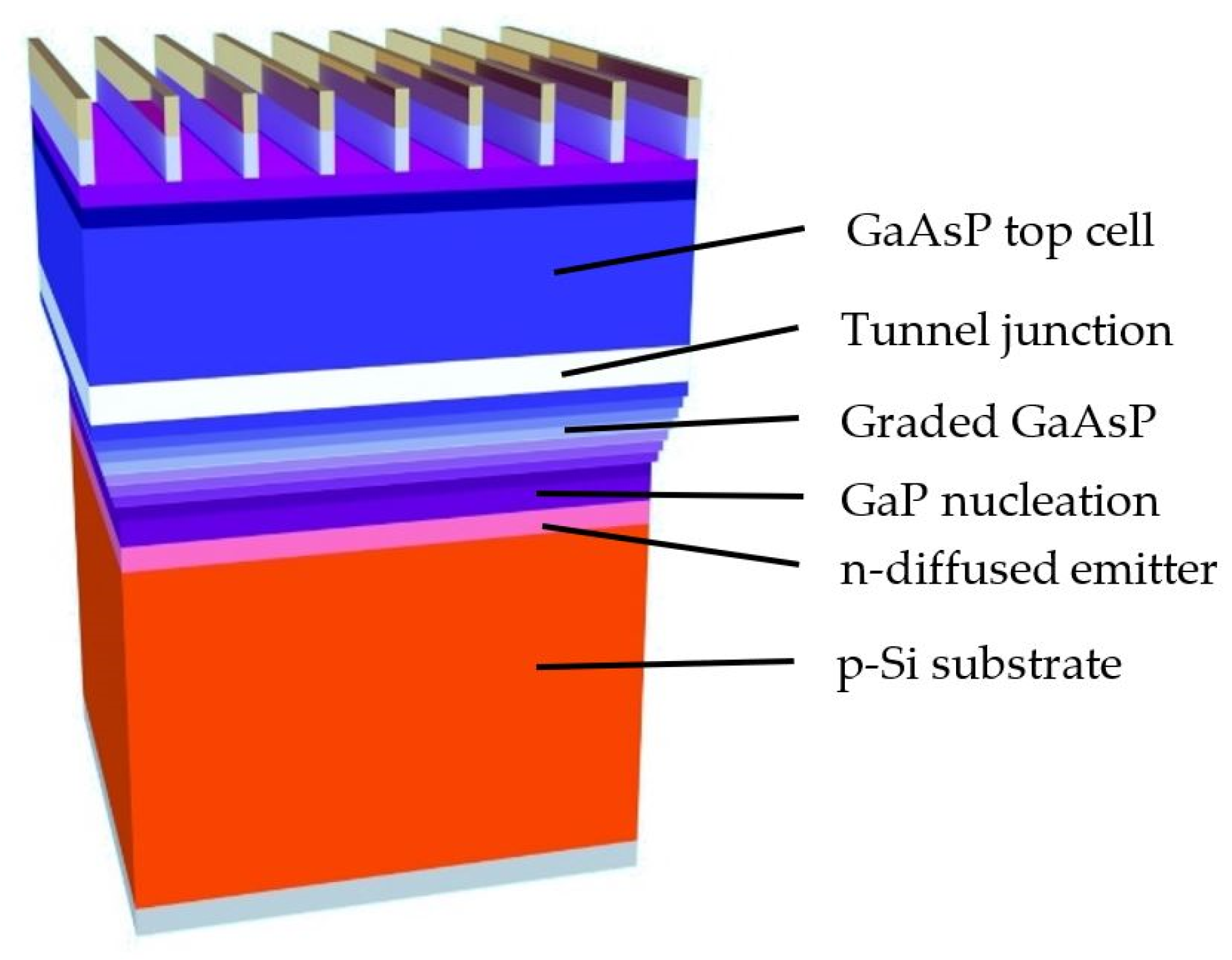
2.2. Process Rationale

In order to implement the routine proposed in any standard MOVPE reactor used for arsenide/phosphide devices, the process should avoid the need of two chambers, ultra-high temperatures and specific precursors. Thus, in our routine the Si homoepitaxy step is omitted, the thermal annealing is carried out at ordinary MOVPE process temperatures for III-As/P semiconductors and the GaP nucleation is conducted using standard precursors with continuous growth mode. Obviously, if compared directly to the optimum routines reported, the proposed routine would come at the price of a lower quality since these procedures do not allow a surface preparation as efficient; the cleaning can be imperfect, and subsequently the GaP nucleation would be carried out on a non-ideal surface. Therefore, we have resorted to an AsH3 pre-exposure prior to the GaP growth, which minimizes the deficiencies of the aforementioned conditions. With this strategy, the nucleation routine rationale (sketched in Figure 2) can be described as follows:
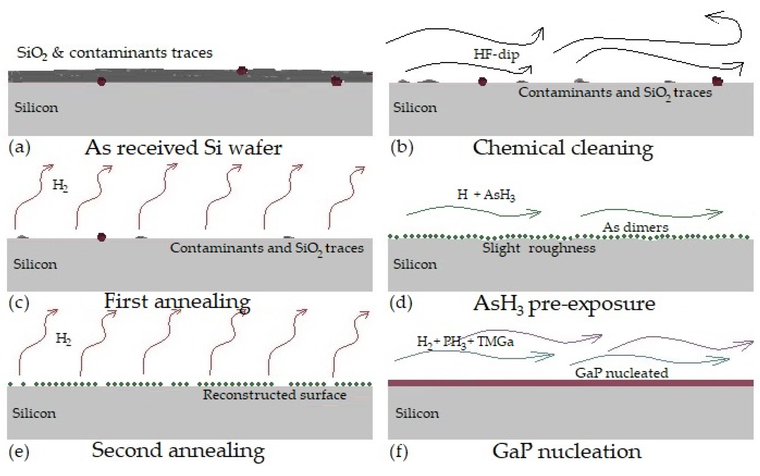
  • Our starting wafer is covered in a native SiO2 layer and may also contain traces of superficial carbonates (Figure 2a);
  • Initially, most of the native oxide on the wafers is removed with an HF-dip and wafers are immediately loaded into the MOVPE reactor (Figure 2b);
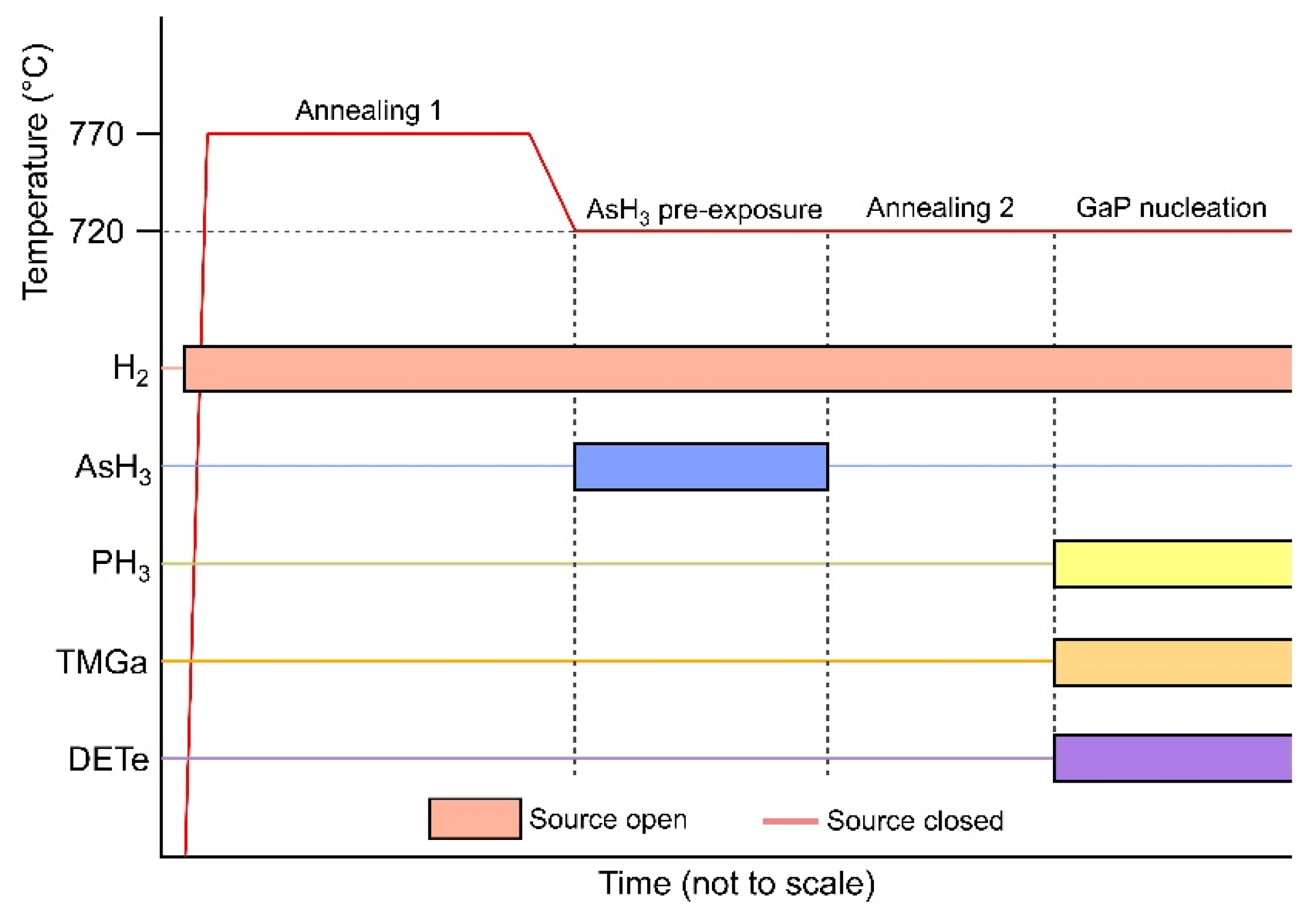
  • Then, the wafers are subjected to a thermal annealing in the MOVPE reactor under H2 ambient at 770 °C, a temperature reachable in most As/P MOVPE tools. This step intends to favor the desorption of traces of the native oxide and superficial carbonates that might have survived the HF dip. It also aims at reaching the ideal surface configuration, consisting of double-stepped terraces (Figure 2c);
  • Afterwards, the wafers are exposed to a short flux of AsH3 (Figure 2d). This so-called pre-exposure step aids in the deoxidation and the elimination of other contaminants as carbon [18,19,20]. In principle, such group-V pre-exposure could be also interesting in order to form a p-n junction for the bottom subcell by the in-diffusion of As into the wafer. However, if the variables of this pre-exposure are not well optimized it can be also detrimental as AsH3 can etch (i.e., roughen) the surface [20,21]. The reason for using AsH3, instead of PH3 that will be used afterwards to grow the GaP, is because As-precursors have shown to be effective removing oxide traces, whilst much less aggressive than PH3 in promoting the silicon surface roughening [19,20,21,22]. Possibly, this is because As-Si bonds are more stable than P-Si or Ga-Si bonds and therefore less Si is exposed to atomic hydrogen [21];
  • As some roughening will inevitably occur after AsH3 exposure, a second annealing under H2 ambient without precursor supply can reconstruct the Si surface [23] and mitigate the roughening created by the pre-exposure step (Figure 2e).
  • The last stage in the routine is the GaP nucleation proper, whose purpose is to create the virtual substrate for subsequent III-V growth. The nucleation conditions must be adapted to optimize the result in the presence of small imperfections on the surface, defects or a non-perfect double-stepped single domain silicon surface.
The different process steps just described and represented in Figure 2a–f involve a considerable number of parameters, including temperature, duration, flow, reactor pressure, V/III ratios, growth rates, ... The systematic analysis of such an immense parameter space is simply undoable. In this respect we reduced the complexity by only exploring parameters in limited ranges. A detailed description of the optimization process is out of the scope of this paper and can be accessed elsewhere [24]. Just as a brief indication, we used in situ measurements using reflectance anisotropy spectroscopy (RAS) and ex situ measurements using AFM to benchmark process conditions. For example, Figure 3 plots RAS signals obtained during our work in an optimization process for the AsH3 pre-exposure. As reported in several works [19,22] on AsH3-exposed Si surfaces, a Si wafer uniformly covered with As dimers consistently oriented forming a single domain, should present a RAS signal with two strong peaks with energies at 2.9–3.4 eV and 3.6–3.9 eV [19,22], and intensities ΔR/R between 1 and 2, depending on wafer miscut and temperature. Hence, any feature that breaks such ideal surface arrangement, namely, contaminants, or surface roughness revealing high index planes should decrease the intensity of such RAS signal. Therefore, to optimize the AsH3 pre-exposure step, we swept temperatures, duration and AsH3 flows in the search for RAS signatures with maximum intensity in both these peaks and then checked ex situ the morphological quality of the surfaces with subsequent AFM analyses. In this line, Figure 3 shows three different RAS signatures corresponding to three different experimental conditions for the pre-exposure where a clear trend towards higher levels of dimerization in a single domain. Experiment #3 (red curve) shows two clear, intense peaks attributed to a strong dimerization oriented in a single domain; whereas Experiment #1 (blue curve) shows only a weak peak at high energies evidencing a much higher degree of surface disorder. The RAS signature of [22] has been added as an example for comparison. It shows the aforementioned peaks but with different intensities and energies, that can be attributed to the different wafer miscut and measurement temperature. Following similar strategies, each step in the process was optimized to conclude with the routine summarized in Table 1 and sketched in Figure 4. It is important to highlight that the reactor pressure has been observed to be a variable of vital importance. It determines the precursor partial pressures and thus the intensity of the surface cleaning/etching during hydride pre-exposures and also dictates the GaP growth mode (i.e., 2D vs. 3D), since it affects the surface mobility of the adatoms nucleating in a more homogeneous way and not gathering in sites more energetically favorable provided by defects.
We would like to finish this section with a final word of caution. The rationale exposed is based on our educated intuition and understanding on how the nucleation process works, which seems to be backed by the experimental results presented in the next section. However, we have a very limited knowledge on what is really happening on the surface in MOVPE during epitaxial growth. Unlike in MBE, where RHEED is an invaluable tool to see the process evolution almost in real time, in MOVPE RAS measurements provide only a partial, indirect and phenomenological vision of the process, so this section should be read as a hypothesis, consistent with the empirical evidence heretofore but not as an unequivocal and empirical proof of how the MOVPE GaP/Si process takes place.

3. Results and Discussion

Samples were grown following the process described in Table 1 and Figure 4 to produce GaP/Si templates. In this section we summarize the morphological, structural and electrical characterization of such samples.

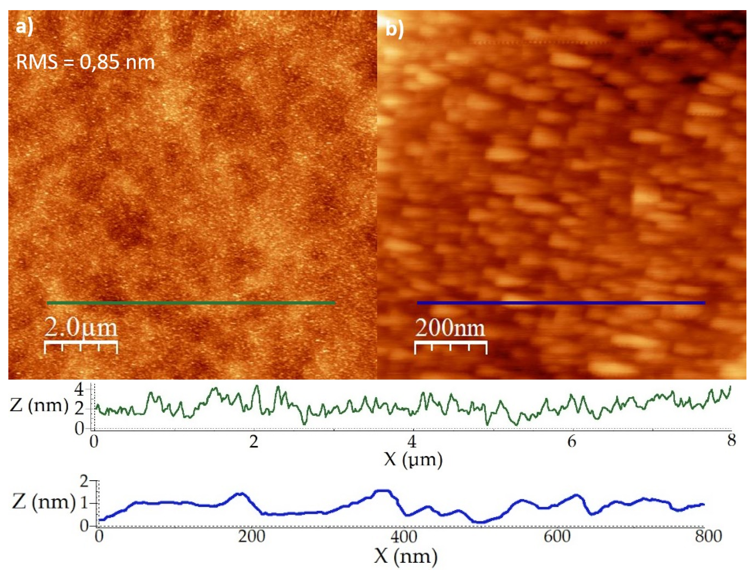
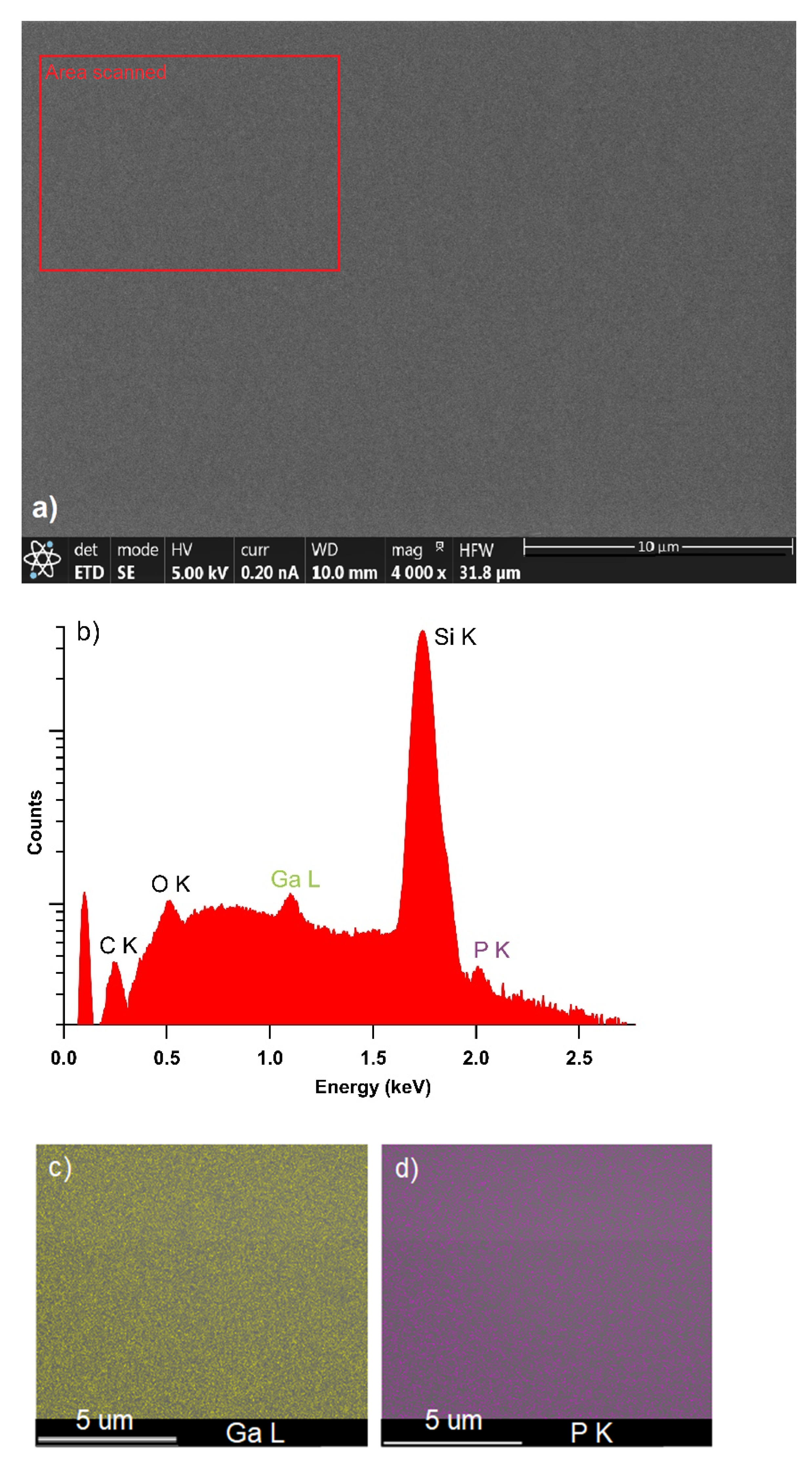
3.1. Surface Morphology: Atomic Force Microscopy (AFM) and Scanning Electron Microscopy (SEM)

Figure 5a,b present typical AFM scans of 10 µm × 10 µm and 1 µm × 1 µm of the surface of our GaP/Si samples. Such figures reveal that the GaP coverage is continuous, without any evidence of voids, hillocks or other 3D features. The root mean square (RMS) roughness measured in our samples ranges from 0.50 to 0.85 nm (depending on scanned area and magnification), which is a reasonably low value for subsequent III-V growth. This value is not record low as in [18], but we have avoided the use of low temperatures for the nucleation, which involves the use of costly precursors (TBAs and TBP). The 1 µm × 1 µm shows some longitudinal faceted features following the wafer steps, as also reported in [25]. Other authors have observed longitudinal features [14]. However, as stated above, our routine is simpler and does not include a Si homoepitaxy step, avoiding the need of two reactors.
Profiles of both AFM scans are represented at the bottom panel in Figure 5 and show relatively smooth variations on the surface. This smooth GaP surface extends across the wafer. Figure 6a includes a SEM image which shows a wider area of the surface. Again a smooth surface is observed, with no trace of defects or undesired features. EDX was employed to assess the homogeneity of the GaP layer. Figure 6b shows one of the EDX spectra from the area boxed in Figure 6a as an example, where P and Ga are detected. Figure 6c,d present the color maps generated from the Ga and P detection, respectively, obtained from the spectra of the selected area. It can be observed that both elements are uniformly spread along the area and thus voids or discontinuities are not present in the GaP film.

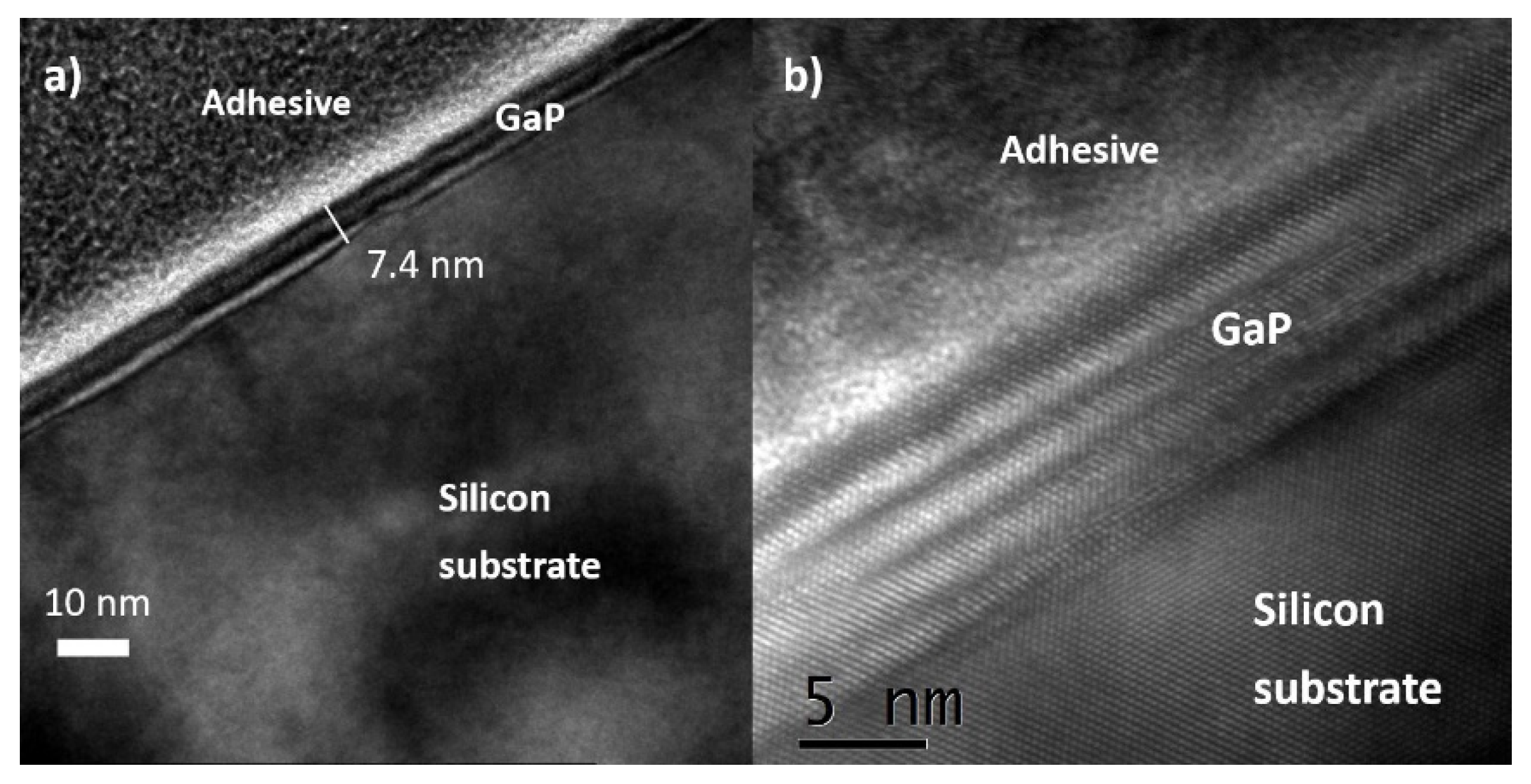
3.2. Cross Section: Transmission Electron Microscopy (TEM)

Figure 6b and Figure 7a show the cross-sectional TEM and HRTEM images of the sample along the [011] direction. The sample presented in this experiment followed the same routine as the one in Figure 5 and Table 1. At first sight it is possible to see that the GaP layer is continuous and homogeneous with a thickness of around 7.4 nm. Some degree of surface roughness is also noticeable in Figure 7a. In the HRTEM image (Figure 7b) there are neither defects observable in the layer—as stacking faults, microtwins or antiphase domains—nor at the GaP/Si interface. Furthermore, no oxides or other contaminants have been detected. Further analysis are needed but, in short, the microstructure revealed in Figure 7b is in agreement with what was observed in other reports on GaP/Si samples [26].

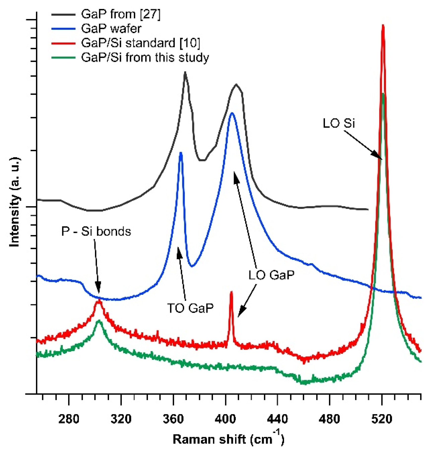
3.3. Layer Quality, Defects and Contaminants: Raman Spectroscopy

Classic XRD analysis is challenging in these samples with only a few nm of GaP. Instead, Raman spectroscopy was measured to confirm the lack of crystallographic defects and impurities by the analysis of the features in the Raman spectra. In this respect, the Raman spectra of our samples have been compared with measurements of state-of-the-art GaP/Si templates using the standard growth [10] and also with bulk GaP wafers. Figure 8 shows such measurements, where the black line represents bulk GaP from [27], the blue line represents the GaP wafer, the red line a GaP/Si sample following the standard routine [10] and the green line the GaP/Si sample from this study.In the GaP wafer (in blue) two peaks are clearly visible that represent the longitudinal and transverse optical vibrations of the GaP in the first order spectrum (labelled TO and LO in the figure, respectively) [28], as in [27], which have been added to confirm such optical vibrations. In the case of both GaP/Si samples, the silicon first-order LO Raman vibration mode is clearly visible at 517–520 cm−1 [29].
In these samples another peak at around 300 cm−1 stands out. The origin of this peak has been associated with Si-P vibrations on low dimensional SiP systems [30]. These bonds have been probably formed during the initial stages of the GaP nucleation. If we compare both samples, the FWHM of this peak is very similar (11.05 cm−1 for the standard sample versus 11.04 cm−1 for the one from this study).
In the GaP/Si sample with standard growth, the LO mode of the GaP is clearly visible with a high quality since the peak is very sharp. On the other hand, none of the two GaP vibration modes are visible in the GaP/Si sample under study. The lack of these peaks could be due to the limited thickness of the layer grown, of around 7.4 nm as observed by TEM [31].
Our goal with this analysis was to detect extra features in the Raman signals in our GaP/Si samples that could be related to defects breaking the crystal symmetry (for example, signature of oxygen bonds, carbon bonds or As bonds) and thus leading to disorder-induced Raman scattering. We have not observed the such, therefore, Raman measurements and the TEM analysis have shown that this GaP layer has nucleated mostly free of defects and contaminants. However, it is important to note that TEM images only cover a very local area in the sample and from them it cannot be concluded that the full wafer has this quality at the GaP/Si interface and GaP layer. On the other hand, Raman measurements have a light beam with a diameter from microns up to millimeters, and the exploration of different zones of the sample can be achieved in shorter times, assessing a wider area of the sample. This fact in conjunction with the very limited surface roughness measured makes this GaP/Si sample –in our opinion– comparable to the state-of-the-art [5].

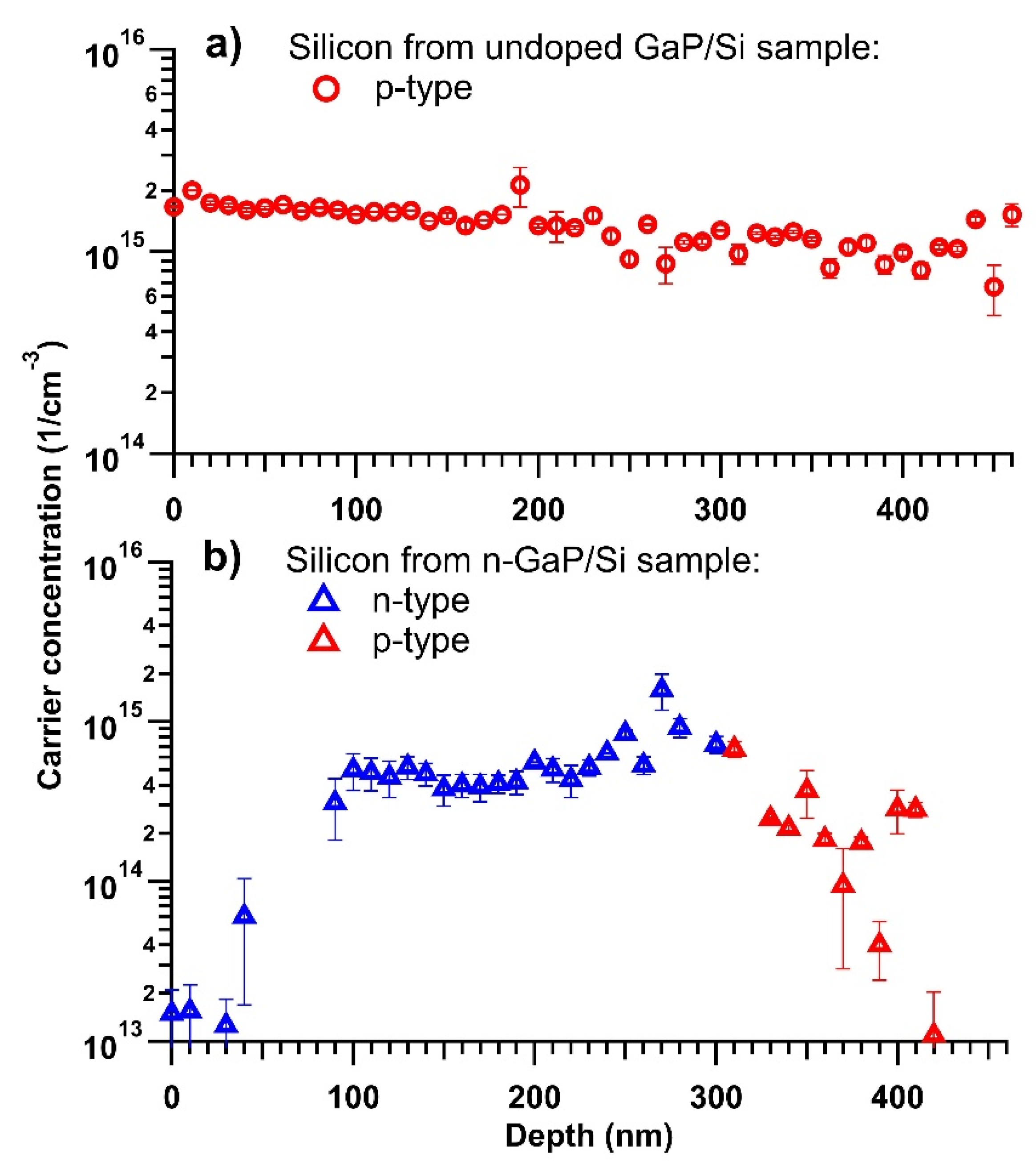
3.4. Group-V Diffusion during the Nucleation Process: p-n Junction Formation

The relatively high temperatures in our process should trigger the diffusion of atoms into the Si wafer [32]. The arsine pre-exposure, the second thermal annealing and GaP nucleation take place at 720 °C, which could be enough for the diffusion of As and P (n-type dopants) and Ga (p-type dopant) into the substrate. Two types of GaP/Si samples were evaluated in these experiments: (1) samples following the process in Table 1; and (2) samples in which the GaP was grown without Te, i.e., nominally undoped. In order to assess the diffusion, the carrier concentration vs. depth in the samples was measured by electro-chemical capacitance voltage (ECV). Figure 9 shows the ECV profiles of both samples, which only include the carrier concentration in the silicon substrate, since the GaP layer was etched off with aqua regia (HNO3:HCl–1:3).
In the nominally undoped GaP samples, where Te was not employed, the ECV measurement (green circles-a) yields a flat line corresponding to the p-type doping of the Si wafer. Therefore, in this case no significant diffusion takes place or, more accurately, diffusion is not intense enough to alter or compensate the boron concentration of the silicon substrate. On the other hand, the samples in which GaP:Te is grown do show a p/n junction with a superficial n-type region extending for around 300 nm. In these samples, the surface electron concentration compensates the p-type background doping and produces a net n-type emitter.
The interpretation of why we only get diffusion when n++ GaP:Te is grown on Silicon is not straightforward. The in-diffusion of Te into the Si wafer is discarded given the low temperatures used and the very low diffusion coefficient of Te in Silicon as compared with the other elements [33]. However, it has been reported that n++ layers are very effective introducing point defects that boost diffusion processes in the structure [34,35], so our interpretation of the process is that vacancies in the GaP:Te layer act as a sink for Si atoms, which in turn create vacancies in the Si wafer that boost the in-diffusion of Ga and P into the wafer. In this respect the intensity of the diffusion process and thus the depth of the emitter could be modulated by adjusting the n-type doping in the GaP [35].
In light of this explanation the particular shape of the emitter profile in Figure 9 can be explained. The carrier concentration presents a first region (<100 nm) where it grows with an initial ramp and then stabilizes in a plateau of ND~5 × 1014 cm−3. This can be explained considering that the net carrier concentration is the result of the balance between the wafer background doping and two diffusion processes: the shallow diffusion of Ga [36], which is a p-type dopant in Si, and the more intense and deeper diffusion of P [37], which is an n-type dopant in Si. Arsenic has lower diffusion coefficient than the others and we consider that its diffusion has a lower effect [37,38]. The net free carrier concentration at each depth will be the result of the competition between these terms. Deep in the sample, the diffusions are negligible and the background p-type doping dominates; between 100 and 300 nm from the surface the diffusion of Ga is negligible, whilst the diffusion of P is strong enough to compensate the wafer doping and produce a net free electron concentration; between 0 and 100 nm diffusion of P is still dominant but several diffusion processes coexist giving rise to the observed initial ramp. An analogous explanation has been proposed to explain similar profiles obtained in Ge solar cells also grown in a MOVPE ambient [39].
In brief, the ECV measurements show that with our reference GaP/Si nucleation routine a p-n junction can be created into the silicon, forming the grounds of a Si bottom cell in a possible GaAsP/Si tandem. In this Si bottom cell, the GaP acts as window layer for the front passivation. Another aspect to be tackled is the rear passivation in these solar cells. It is known that MOVPE growth environments can degrade the lifetime of silicon wafers as a result of metallic impurities diffusing into the wafer from the heated graphite susceptor [40]. This effect can be minimized if the rear side of the wafer is protected with Si3N4 during the MOVPE growth [41]. Further analysis and experiments are being carried out to optimize this solar cell, together with the rest of the III-V growth.

4. Conclusions

A GaP on Si nucleation routine has been developed to combine the high efficiency of III-V semiconductors with the low cost of silicon substrates. This routine intends to be as simple as possible to integrate III-V multijunction solar cells on Si using and scalable process. For this purpose, this nucleation routine combines the nucleation of a GaP layer with the creation of a Si bottom cell in a single-run, using a conventional MOVPE reactor equipping standard precursors. The process includes a previous ex situ substrate preparation by means of an HF dip, and in situ steps in the MOVPE reactor involving thermal anneals, an AsH3 pre-exposure, and the nucleation itself. The characterization has shown a GaP layer with a smooth surface, state-of-the-art crystal quality and free of defects, contaminants and oxide. Moreover, it has been observed that the use of n-type doping in the GaP layer is the trigger for the formation of a p-n junction for the Si bottom cell.
The manufacturing of the Si bottom cell to assess its photovoltaic behavior is currently being carried out. The next steps in the research encompass the calibration of the emitter creation by in-diffusion by tuning the n-dopant flows and the thermal load. The rear passivation of the silicon also needs to be studied. The remaining III-V layers will be grown, which includes the GaAsxP1−x graded buffer, and the GaAsP top cell, to form the dual-junction III-V/Si solar cell.

Author Contributions

Conceptualization, P.C. and I.R.-S.; methodology, P.C. and I.R.-S.; software, P.C.; validation, all authors; formal analysis, P.C. and I.R.-S.; investigation, P.C. and I.R.-S.; resources, I.R.-S.; data curation, P.C.; Writing—Original draft preparation, P.C.; Writing—Review and editing, all authors; visualization, P.C.; supervision, I.R.-S.; project administration, I.R.-S.; funding acquisition, I.R.-S. All authors have read and agreed to the published version of the manuscript.

Funding

This work was supported by the Spanish Ministerio de Ciencia e Innovación through project VIGNEMALE [grant number RTI2018-094291-B-I00] and DAMAINSOL [grant number RTI2018-101020-B-I00].

Data Availability Statement

The data presented in this study are available on request from the corresponding author. The data are not publicly available due to privacy.

Acknowledgments

We acknowledge the assistance in the AFM provided by the “New concepts for solar cells” group and the “Centro nacional de microscopía electronica” of the Universidad Complutense de Madrid.

Conflicts of Interest

The authors declare no conflict of interest. The funders had no role in the design of the study; in the collection, analyses, or interpretation of data; in the writing of the manuscript, or in the decision to publish the results.

CAS Numbers of Chemical Elements

Silicon (CAS7440-21-3), Gallium (CAS7440-55-3), Phosphorus (CAS7723-14-0), Arsenic (CAS7440-38-2), Tellurium (CAS13494-80-9), Germanium (CAS7440-56-4).

References

  1. Battaglia, C.; Cuevas, A.; De Wolf, S. High-efficiency crystalline silicon solar cells: Status and perspectives. Energy Environ. Sci. 2016, 9, 1552–1576. [Google Scholar] [CrossRef] [Green Version]
  2. Yoshikawa, K.; Yoshida, W.; Irie, T.; Kawasaki, H.; Konishi, K.; Ishibashi, H.; Asatani, T.; Adachi, D.; Kanematsu, M.; Uzu, H.; et al. Exceeding conversion efficiency of 26% by heterojunction interdigitated back contact solar cell with thin film Si technology. Sol. Energ Mater. Sol. Cells 2017, 173, 37–42. [Google Scholar] [CrossRef]
  3. Shockley-Queisser, W.H. Detailed balance limiy of efficiency of p-n junction solar cells. J. Appl. Phys. 1961, 32, 510–519. [Google Scholar] [CrossRef]
  4. Geisz, J.F.; France, R.M.; Schulte, K.L.; Steiner, M.A. Six-junction III–V solar cells with 47.1% conversion efficiency under 143 Suns concentration. Nat. Energy 2020, 5, 326–335. [Google Scholar] [CrossRef]
  5. Hayashi, K.; Soga, T.; Nishikawa, H.; Jimbo, T.; Umeno, M. MOCVD growth of GaAsP on Si for tandem solar cell application. In Proceedings of the 1994 IEEE 1st World Conference on Photovoltaic Energy Conversion-WCPEC (A Joint Conference of PVSC, PVSEC and PSEC), Waikoloa, HI, USA, 5–9 December 1994. [Google Scholar]
  6. Supplie, O.; Romanyuk, O.; Koppka, C.; Steidl, M.; Nägelein, A.; Paszuk, A.; Winterfeld, L.; Dobrich, A.; Kleinschmidt, P.; Runge, E.; et al. Metalorganic vapor phase epitaxy of III–V-on-silicon: Experiment and theory. Prog. Cryst. Growth Charact. Mater. 2018, 64, 103–132. [Google Scholar] [CrossRef]
  7. Caño, P.; Hinojosa, M.; Nguyen, H.; Morgan, A.; Fuertes Marrón, D.; García, I.; Johnson, A.; Rey-Stolle, I. Hybrid III-V/SiGe solar cells grown on Si substrates through reverse graded buffers. Sol. Energy Mater. Cells 2020, 205, 110246. [Google Scholar] [CrossRef]
  8. Olson, J.M.; Al-Jassim, M.M.; Kibbler, A.; Jones, K.M. MOCVD growth and characterization of GaP on Si. J. Cryst. Growth 1986, 77, 515–523. [Google Scholar] [CrossRef]
  9. Narayanan, V.; Sukidi, N.; Hu, C.; Dietz, N.; Bachmann, K.J.; Mahajan, S.; Shingubara, S. Growth of gallium phosphide layers by chemical beam epitaxy on oxide patterned (001) silicon substrates. Mater. Sci. Eng. B 1998, 54, 207–209. [Google Scholar] [CrossRef]
  10. Volz, K.; Beyer, A.; Witte, W.; Ohlmann, J. GaP-nucleation on exact Si (001) substrates for III/V device integration. J. Cryst. Growth 2011, 315, 37–47. [Google Scholar] [CrossRef]
  11. Feifel, M.; Ohlmann, J.; Benick, J.; Rachow, T. MOVPE grown gallium phosphide-silicon heterojunction solar cells. IEEE J. Photovolt. 2017, 7, 502–507. [Google Scholar] [CrossRef]
  12. García-Tabarés, E.; Martín, D.; García, I.; Lelievre, J.F.; Rey-Stolle, I. Optimization of the silicon subcell for III-V on silicon multijunction solar cells: Key differences with conventional silicon technology. AIP Conf. Proc. 2012, 1477, 5–9. [Google Scholar]
  13. Connolly, J.P.; Mencaraglia, D.; Renard, C.; Bouchier, D. Designing III–V multijunction solar cells on silicon. Prog. Photovolt. Res. Appl. 2014, 22, 810–820. [Google Scholar] [CrossRef]
  14. Grassman, T.J.; Carlin, J.A.; Galiana, B.; Yang, L.M. Nucleation-related defect-free GaP/Si (100) heteroepitaxy via metal-organic chemical vapor deposition. Appl. Phys. Lett. 2013, 102, 142102. [Google Scholar] [CrossRef] [Green Version]
  15. Grassman, T.J.; Lepkowski, D.L.; Boyer, J.T.; Chmielewski, D.J.; Yi, C.; Western, N.; Mehrvarz, H.; Ho-Baillie, A.; Kerestes, C.; Derkacs, D.; et al. Toward >25% Efficient Monolithic Epitaxial GaAsP/Si Tandem Solar Cells. In Proceedings of the 2019 IEEE 46th Photovoltaic Specialists Conference (PVSC), Chicago, IL, USA, 16–21 June 2019. [Google Scholar]
  16. Kunert, B.; Németh, I.; Reinhard, S.; Volz, K.; Stolz, W. Si (001) surface preparation for the antiphase domain free heteroepitaxial growth of GaP on Si substrate. Thin Solid Film. 2008, 517, 140–143. [Google Scholar] [CrossRef]
  17. Beyer, A.; Ohlmann, J.; Liebich, S.; Heim, H.; Witte, G.; Stolz, W.; Volz, K. GaP heteroepitaxy on Si (001): Correlation of Si-surface structure, GaP growth conditions, and Si-III/V interface structure. J. Appl. Phys. 2012, 111, 083534. [Google Scholar] [CrossRef]
  18. Paszuk, A.; Supplie, O.; Kim, B.; Brückner, S.; Nandy, M.; Heinisch, A.; Kleinschmidt, P.; Nakano, Y.; Sugiyama, M.; Hannappel, T. GaAsP/Si tandem solar cells: In situ study on GaP/Si: As virtual substrate preparation. Sol. Energy Mater. Sol. Cells 2018, 180, 343–349. [Google Scholar] [CrossRef]
  19. Warren, E.; Kibbler, A.; France, R.; Norman, A.; Stradins, P.; McMahon, W. Growth of antiphase-domain-free GaP on Si substrates by metalorganic chemical vapor deposition using an in situ AsH3 surface preparation. Appl. Phys. Lett. 2015, 107, 82109. [Google Scholar] [CrossRef]
  20. Hannappel, T.; McMahon, W.E.; Olson, J.M. An RDS, LEED, and STM Study of MOCVD-Prepared Si (100) surfaces. J. Cryst. Growth 2004, 272, 24–29. [Google Scholar] [CrossRef]
  21. García-Tabarés Valdivieso, E. MOVPE Growth of III-V Semiconductors on Silicon for Third Generation Solar Cells. Ph.D. Thesis, Universidad Politécnica de Madrid, Madrid, Spain, 2015. [Google Scholar]
  22. Paszuk, A. Controlling Si (111) and Si (100) Surfaces for Subsequent GaP Heteroepitaxy in CVD Ambient. Ph.D. Thesis, Technische Universität Ilmenau, Ilmenau, Germany, 2017. [Google Scholar]
  23. Paszuk, A.; Dobrich, A.; Koppka, C.; Brückner, S.; Duda, M.; Kleinschmidt, P.; Supplie, O.; Hannappel, T. In situ preparation of Si p-n junctions and subsequent surface preparation for III-V heteroepitaxy in MOCVD ambient. J. Cryst. Growth 2017, 464, 14–19. [Google Scholar] [CrossRef]
  24. Caño, P. Desarrollo de Células Solares Multiunión de Semiconductores del Grupo III-V Sobre Sustratos de Silicio. Ph.D. Thesis, Universidad Politécnica de Madrid, Madrid, Spain, 2021. [Google Scholar]
  25. Warren, E.L.; Kibbler, A.E.; France, R.M.; Norman, A.G.; Olson, J.M.; McMahon, W.E. Investigation of GaP/Si heteroepitaxy on MOCVD prepared Si (100) surfaces. In Proceedings of the 2015 IEEE 42nd Photovoltaic Specialist Conference (PVSC), New Orleans, LA, USA, 14–19 June 2015. [Google Scholar]
  26. Navarro, A.; García-Tabarés, E.; Galiana, B.; Caño, P.; Rey-Stolle, I.; Ballesteros, C. MOVPE growth of GaP on Si with as initial coverage. J. Cryst. Growth 2017, 464, 8–13. [Google Scholar] [CrossRef]
  27. Pelosi, C.; Musaeva, N.; Attolini, G.; Bosi, M.; Clerjaud, B.; Bénalloul, P.; Barthou, C.; Jabbarov, R.B.; Abdullayeva, S. Heteroepitaxial Movpe Growth of GaInPN Alloys on Si. In Proceedings of the First International Conference on Material and Information Sciences in High Technologies MISHT-2007, Bakou, Azerbaijan, 26–29 September 2007. [Google Scholar]
  28. Russell, J.P. Raman spectroscopy using a gas laser. J. Phys. 1965, 56, 620–626. [Google Scholar] [CrossRef]
  29. Dolling, G.; Cowley, R.A. The thermodynamic and optical properties of germanium, silicon, diamond and gallium arsenide. Proc. Phys. Soc. 1966, 88, 463. [Google Scholar] [CrossRef]
  30. Li, C.; Wang, S.; Li, C.; Yu, T.; Jia, N.; Quiao, J.; Zhu, M.; Liu, D.; Tao, X. Highly sensitive detection of polarized light using a new group IV–V 2D orthorhombic SiP. J. Mater. Chem. C 2018, 6, 7219–7225. [Google Scholar] [CrossRef]
  31. Bondi, A.; Cornet, C.; Boyer, S.; Nguyen, T.; Létoublon, A.; Pedesseau, L.; Durand, O.; Moreac, A.; Ponchet, A.; Le Corre, A.; et al. Raman investigation of GaP–Si interfaces grown by molecular beam epitaxy. Thin Solid Film. 2013, 541, 72–75. [Google Scholar] [CrossRef]
  32. García-Tabarés, E.; Martín, D.; García, I.; Rey-Stolle, I. Understanding phosphorus diffusion into silicon in a MOVPE environment for III–V on silicon solar cells. Sol. Energy Mater. Sol. Cells 2013, 116, 61–67. [Google Scholar] [CrossRef] [Green Version]
  33. Janzén, E.; Grimmeiss, H.G.; Lodding, A.; Deline, C. Diffusion of telluriom dopant in silicon. J. Appl. Phys. 1982, 53, 7367–7371. [Google Scholar] [CrossRef]
  34. Deppe, D.G.; Plano, W.E.; Baker, J.E.; Holonyak Jr., N. Comparison of SiIII-SiV and SiIII-VIII diffusion models in III-V heterostructures lattice matched to GaAs. Appl. Phys. Lett. 1988, 53, 2211. [Google Scholar] [CrossRef]
  35. Hinojosa, M.; García, I.; Dadgostar, S.; Algora, C. Point-Defects Assisted Zn-Diffusion in AlGaInP/GaInP Systems during the MOVPE Growth of Inverted Multijunction Solar Cells. IEEE J. Photovolt. 2021, 11, 429–436. [Google Scholar] [CrossRef]
  36. Haridoss, S.; Bénière, F.; Gauneau, M.; Rupert, A. Diffusion of gallium in silicon. J. Appl. Phys. 1980, 51, 5833–5837. [Google Scholar] [CrossRef]
  37. Jones, S.W. Diffusion in Silicon; IC Knowledge LCC: Georgetown, MA, USA, 2008. [Google Scholar]
  38. Ohkawa, S.; Nakajima, Y.; Fukukawa, Y. Arsenic diffusion into silicon from elemental source. Jpn. J. Appl. Phys. 1975, 14, 458. [Google Scholar] [CrossRef]
  39. Barrigón, E.; Ochoa, M.; García, I.; Barrutia, L.; Algora, C.; Rey-Stolle, I. Degradation of Ge subcells by thermal load during the growth of multijunction solar cells. Prog. Photovolt. Res. Appl. 2018, 26, 102–111. [Google Scholar] [CrossRef] [Green Version]
  40. García-Tabarés, E.; Carlin, J.A.; Grassman, T.J.; Martín, D.; Rey-Stolle, I.; Ringel, S.A. Evolution of silicon bulk lifetime during III–V-on-Si multijunction solar cell epitaxial growth. Prog. Photovolt. Res. Appl. 2015, 24, 634–644. [Google Scholar] [CrossRef] [Green Version]
  41. Feifel, M.; Rachow, T.; Benick, J.; Ohlmann, J. Gallium phosphide window layer for silicon solar cells. IEEE J. Photovolt. 2016, 6, 384–390. [Google Scholar] [CrossRef]
Figure 1. Structure of the tandem GaAsP/Si solar cell that is the target of this research. The widths of the figure represent schematically the lattice constant.
Coatings 11 00398 g001
Figure 2. Different steps of the routine designed in this research: (a) Si wafer as received with native oxide and contaminants; (b) Chemical cleaning with a HF-dip; (c) Annealing in the reactor chamber under H2; (d) AsH3 pre-exposure; (e) Second annealing under H2; (f) GaP nucleation.
Coatings 11 00398 g002
Figure 3. Reflectance anisotropy spectroscopy (RAS) of AsH3 exposed Si (100) wafers under different experimental conditions. In dashed grey line the RAS signature from [22] is added for comparison.
Coatings 11 00398 g003
Figure 4. Diagram summarizing the routine developed for the GaP nucleation on Si.
Coatings 11 00398 g004
Figure 5. 10 µm × 10 µm (a) and 1 µm × 1 µm (b) AFM image of the GaP/Si sample. The green and blue lines show the profiles in both scans.
Coatings 11 00398 g005
Figure 6. (a) SEM image of 30 µm × 30 µm; (b) EDX spectra from scanned area; (c,d) color maps from scanned area that represent Ga and P signals, respectively.
Coatings 11 00398 g006
Figure 7. TEM images of the GaP nucleated on Si that followed the routine of the sample of Figure 5 of 100 nm × 100 nm (a) and 40 nm × 40 nm (b).
Coatings 11 00398 g007
Figure 8. Raman spectroscopy of GaP samples. In black: GaP from [27]. In blue: bulk GaP. In red: GaP/Si template from [5]. In purple: GaP nucleated on Si under study.
Coatings 11 00398 g008
Figure 9. Electro-chemical capacitance voltage (ECV) of silicon substrates as a function of the depth, on which a GaP (a) or GaP:Te (b) were grown on top after the substrate preparation. These layers were etched for measuring the n-dopants diffusion into the silicon substrate.
Coatings 11 00398 g009
Table 1. Summary of the process variables of our GaP/Si nucleation routine. All times are indicated with format mm:ss (minutes:seconds); slpm stands for standard litters per minute; sccm stands for standard cubic centimeters per minute.
SubstrateSi (100)
Miscut4°→ [111]
Chemical cleanHF dip, 3:00
Process pressure250 mbar
Carrier gas and flowH2, 15 slpm
First anneal (T, t)770 °C, 30:00
AsH3 pre-exposure (T, t, flow)720 °C, 2:45, AsH3 = 30 sccm
Second anneal (T, t)720 °C, 2:00
GaP growth (T, t, V/III, flows)720 °C, 0:30, 1500
PH3 = 500 sccm; TMGa = 5 sccm; DETe = 33 sccm
Publisher’s Note: MDPI stays neutral with regard to jurisdictional claims in published maps and institutional affiliations.

