Abstract
Cesium-containing triple cation perovskites are attracting significant attention as suitable tandem partners for silicon solar cells. The perovskite layer of a solar cell must strongly absorb the visible light and be transparent to the infrared light. Optical transmittance measurements of perovskite layers containing different cesium concentrations (0–15%) were carried out on purpose to evaluate the utility of the layers for the fabrication of monolithic perovskite/silicon tandem solar cells. The transmittance of the layers weakly depended on cesium concentration in the infrared spectral range, and it was more than 0.55 at 997 nm wavelength. It was found that perovskite solar cells containing 10% of cesium concentration show maximum power conversion efficiency.
1. Introduction
The promising features of a perovskite/silicon tandem solar cell have attracted considerable attention in recent years [1,2,3,4,5,6,7,8,9,10,11,12,13,14,15]. The interest is inspired by the rapid rise of power conversion efficiency (PCE) of a perovskite solar cell from below 3.8% to more than 25.2% in the last decade [16,17]. Moreover, it is known that the crystalline silicon solar cell has demonstrated a certified power conversion efficiency of 26.6% [18,19] which is close to its theoretical efficiency limit of 33.3% [20]. The efficiency of a solar cell is limited by effective use of photons having energy close to the forbidden energy gap. Photons with higher energies create electron–hole pairs, and the excess energy is transmitted to carriers thus, making them the hot carriers. The heating of charge carriers by light leads to the formation of a thermoelectromotive force of hot carriers having a polar opposite to that of the classical photovoltage caused by the electron–hole pair generation [21,22]. As a result, the creation of hot carriers reduces the PCE of a single-junction solar cell [23]. The coating of a silicon solar cell with a thin perovskite layer absorbing high energy photons allows to considerably decrease the negative effect of the hot carriers.
There are different configurations of tandem solar cells. In the two-terminal (2T) configuration, both solar cells are monolithically integrated [4,5,6,7,8,9,10,13], while in the four-terminal (4T) configuration, the two cells are joined together mechanically [20,24,25,26,27]. The basic requirements for each configuration are the same: the perovskite layer must be a good absorber of the visible light and must be transparent to the infrared light [17].
In recent years, various technologies and methods have been developed to improve PCE and other properties of the perovskite sub-cell. The high-quality performance of a perovskite solar cell can be primarily attributed to its excellent optical properties such as its high absorption coefficient allowing to use a thin film, high defect tolerance, high carrier mobility, and long carrier diffusion length [17,26,27,28,29,30]. Excellent bandgap tunability allows to use a perovskite layer as a top sub-cell on any bottom cell [31,32,33,34]. Currently, the best perovskite solar cells use a mixture of formamidinium (FA) and methylammonium (MA) as the monovalent cations [35,36,37,38,39,40,41]. Thea addition of cesium makes the triple cation perovskite compositions more thermally stable, as they have less phase impurities and are less sensitive to processing conditions [27,35]. The incorporation of cesium was shown to reduce the trap density and charge recombination rates in the perovskite layer [42]. Triple (Cs/FA/MA) cation-based perovskite materials exhibited average PCE fairly exceeding 20% with a stable performance against the long-time exposure to ambient atmosphere [43]. Triple cation perovskites of the generic form “Csx(MA0.17FA0.83)(1−x)Pb(I0.83Br0.17)3“ developed in [35] can be suitable candidates as tandem companions for silicon solar cells.
In this paper, we present an experimental study of structure and optical properties of perovskite Csx(MA0.17FA0.83)(1−x)Pb(I0.83Br0.17)3 layers having different cesium concentration as well as photoelectric properties of solar cells fabricated on their base.
2. Perovskite Cell Fabrication and Characterization
To fabricate efficient perovskite cells, methods and procedures proposed and detailed in Refs. [35,43,44] were used. Glass substrates of 25 × 25 mm2 size coated with fluorine-doped tin oxide (FTO) layer (TEC 10 (3.3 mm), Ossila, Sheffield, UK) were used for the formation of the perovskite cell. Before the formation of the cell, a ~5 mm wide strip of FTO layer was removed (etched) from one edge of the glass substrate. Zn powder and 4 M HCl solution were used for FTO etching. These and other precursors, unless otherwise noted, were from Sigma-Aldrich. After FTO etching, the substrates were cleaned for 20 min with 2% Helmanex solution in an ultrasonic bath (S40 H, Elmasonic, Singen, Germany). Then, the substrates were several times rinsed thoroughly with deionized water and ultrasonicated in isopropanol for 20 min. The substrates were dried by compressed Ar flow and treated for ~5 min in a low-pressure oxygen plasma cleaner (Atto, Diener electronic GmbH + Co. KG, Ebhausen, Germany). A ~30 nm-thick layer of a compact (dense) TiO2 was formed on the substrates by spraying a solution composed of titanium diisopropoxide (bis) acetylacetonate (Ti (acac)2OiPr2) and isopropanol (1:9 vol. ratio) and then sintering it for 15 min at 450 °C on a hotplate (PZ 28-3T Prazitherm, Gestigkeit GmbH, Düsseldorf, Germany). The sintered TiO2-coated substrates were left on the hotplate for ~6 h for natural cooling. After the cooling, a spin-coating method was used to deposit a 150–220 nm-thick layer of a mesoporous TiO2 on the compact TiO2 layer. The mesoporous TiO2 layer was grown using a 30 nm TiO2 particle paste (Dyesol 30NRD/ethanol) diluted in ethanol at a 1:6 wt. ratio. One hundred and fifty microliters (150 µL) of the prepared TiO2 solution was pipetted with an automatic pipette (Eppendorf Research Plus, Eppendorf AG, Hamburg, Germany) on the surface of the substrate placed on a centrifuge table (SPIN 150i POLOS, SPS-Europe B.V.), and the following spinning program was started: 4000 rpm for 20 s with an acceleration of 2000 rpm/s. The mesoporous TiO2 was formed by sintering the layer in a dry air for 30 min at 450 °C. Then, the sample was cooled down to 150 °C and immediately placed into a glovebox (MBRAUN MB-10-G, M. Braun Inertgas-Systeme GMBH, Garching bei München, Germany) with controlled atmosphere (relative humidity ≤0.5 ppm of N2 was continuously maintained). The perovskite structures were grown on mesoporous TiO2 by a one-step precipitation method from the prepared precursor’s solution. As a solvent, a mixture of anhydrous N, N-dimethylformamide (DMF) and dimethylsulfoxide (DMSO) was used: the vol. ratio of components was 4:1. The contents of the precursors in the prepared DMF/DMSO mixture was: 1.1~1.3 M of PbI2, 0.2 M of PbBr, 1 M of Formamidinium iodide (FAI), 0.2 M of Methylammonium bromide (MABr). Then, Cs ions were added to the prepared precursor’s solution: as a source of Cs a 1.5 M CsI solution in DMSO was used. Concentration of CsI in the precursor’s solution was varied from 0 to 15%. According to the literature, the solution of this composition was used to form a perovskite Csx(FA83MA17)(1−x)Pb(I83Br17)3 compound [44]. To deposit the perovskite layer on the formed mesoporous TiO2, the sample was placed on a centrifuge table, and 150 µL of the prepared precursor’s solution was dropped with an Eppendorf pipette. Then, immediately the spin program consisting of two steps was initiated. At the first step, a spinning at 1000 rpm for 10 s with an acceleration of 200 rpm/s was applied. The parameters of the second step were 6000 rpm for 30 s with an acceleration of 1000 rpm/s. Before ending the spin-coating program (~10 s), 150 µL of chlorobenzene (CB) were dropped on the surface of the sample to remove residuals of the solution. The samples were then transferred from the centrifuge table on a hotplate (Isotemp Fisherbrand, Thermo Fisher Scientific, Waltham, MA, USA) and annealed under an inert atmosphere for 60 min at 100 °C. After the annealing and natural cooling for ~10 min, a hole transport layer covering the perovskite layer was formed. The samples were placed again on a centrifuge table, poured with 150 µL of 70 mM 2-N,2-N,2-N′,2-N′,7-N,7-N,7-N′,7-N′-octakis(4-methoxyphenyl)-9,9′-spirobi[fluorene]-2,2′,7,7′-tetramine (Spiro-OMeTAD) solution and immediately an appropriate spin-coating program was initiated (4000 rpm for 25 s with an acceleration of 2000 rpm/s). Before this procedure, 17 µL of Li-bis(trifluoromethylsulfonyl)imide (Li-TFSI) salt in anhydrous acetonitrile and 28.8 µL of 4-tert-butylpyridine (TBP) solution were added to the Spiro-OMeTAD solution. Li-TFSI concentration in the solvent was 10 mgmL−1. The formed perovskite cells were turned dark immediately after preparation and kept in Ar atmosphere with humidity <1%.
The morphology and the thickness of the formed cell layers were examined by means of a scanning electron microscope (SEM) (Helios NanoLab 650, FEI, Hillsboro, OR, USA). The chemical composition of the layers was determined with an attached energy dispersive X-ray spectrometer (EDX) (INCA Energy, Oxford Instruments, Abingdon, UK).
An X-ray diffraction (XRD) method was used to study crystallographic structure of the formed perovskite layers. The measurements were performed with X-ray diffractometer (SmartLab HR-XRD, Rigaku, Tokyo, Japan) equipped with 9 kW power rotating Cu anode X-ray source and theta/theta goniometer. To enable the investigation of thin perovskite layers and to reduce the influence of the substrate, the grazing incidence diffraction geometry with an incidence angle of Cu Kα beam set to 0.5° was applied. The XRD patterns were measured with Bragg–Brentano geometry in 2Θ range of 10°–55°.
Optical transmission spectra of the formed perovskite layers were measured in the wavelength range of 300–1100 nm using AvaSpec ULS2048XL spectrometer and AvaLight-DH-S deuterium–halogen light source (both from Avantes, Apeldoorn, The Netherlands). During the measurements, a 50 ms integration time and an averaging of 100 measured spectra were used.
To measure the efficiency of the formed perovskite cells, these were supplied with ~70 nm-thick Au contacts of special configuration by means of thermal evaporation in the vacuum chamber of VAKSIS PVD Vapor-5S_Th (Vaksis R&D and Engineering, Ankara, Turkey). Schematic cross section of the perovskite solar cell and the microphotograph of the contacts on the top of Spiro-OMeTAD and FTO are presented in Figure 1.
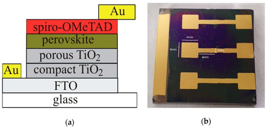
Figure 1.
(a) Schematic cross section of the perovskite solar cell; (b) top view microphotograph of the perovskite solar cell.
Direct current–voltage characteristics and spectra of the perovskite solar cell were measured using Keithley 2602A (Keithley Instruments Inc., Cleveland, OH, US) equipment, and 100 mW/cm2 irradiance was achieved by a AM 1.5 spectral lamp (Newport model 67005, Newport Corp., Irvine, CA, US) placed at an appropriate distance.
Continuous wave photoluminescence spectra were measured by means of a usual photoluminescence setup with completely automated 1 m focal length monochromator (FHR–1000, Horiba Jobin Yvon, Kyoto, Japan), thus achieving 0.8 nm/mm spectra dispersion. For most measurements, the resolution of the photoluminescence system was 0.3 meV at the spectrum maximum and it did not exceed 0.8 meV at the lowest power of excitation. An Ar-ion laser emitting 2.2–2.7 eV photons used for excitation, and its power was varied either by means of the power supply or using neutral glass filters. The diameter of the laser spot on the surface of the sample was 2.5 mm. The photoluminescence was detected by a thermoelectrically cooled gallium arsenide photomultiplier (H7421–50, Hamamatsu, Hamamatsu City, Japan) operating in a photon counting regime.
Time resolved photoluminescence experiments were carried out using a pulsed 532 nm diode pumped solid state (DPSS) microchip laser (photon energy 2.3 eV, pulse full width at a half maximum (FWHM) 400 ps, repetition rate 10 kHz, the spot diameter 0.5 mm). The photoluminescence was detected by a thermoelectrically cooled high-efficiency extended-red multi-alkali cathode photomultiplier (PMC-100-20, Becker&Hickl, Berlin, Germany) with an internal GHz preamplifier. The transient photoluminescence was measured with a time correlated single photon counting system.
3. Results and Discussion
The influence of the added Cs ions on the structure of the formed perovskite layers was studied by the XRD method. It should be mentioned that at this stage of investigation, the perovskites were not coated with the hole transporting layer by reason of the higher accuracy and convenience of the XRD analysis. The measured XRD patterns of the perovskite layers formed from the solutions without CsI and those containing 5, 10 and 15% of CsI are shown in Figure 2. Pronounced peaks at all the XRD patterns unambiguously indicate a clear crystalline structure. In the sample without Cs, the increased intensity of the peaks at 100 and 200 shows prevailing the orientation of perovskite crystallites in (100) direction (the lowest pattern in Figure 2). The addition of Cs cations to the perovskite leads to slight shift of these peaks to higher 2Θ values. Modest amount of Cs changes the prevailing orientation of the crystallites from (100) to (110) (pattern 2 in Figure 2). However, a further increase in Cs concentration up to 15% makes the orientation (100) prevailing again. The analysis of the XRD results shows that the studied perovskite layers have a cubic crystal lattice. The determined lattice parameter a of the perovskite layers with different Cs content as well as an average size of the crystallites D are presented in Table 1.
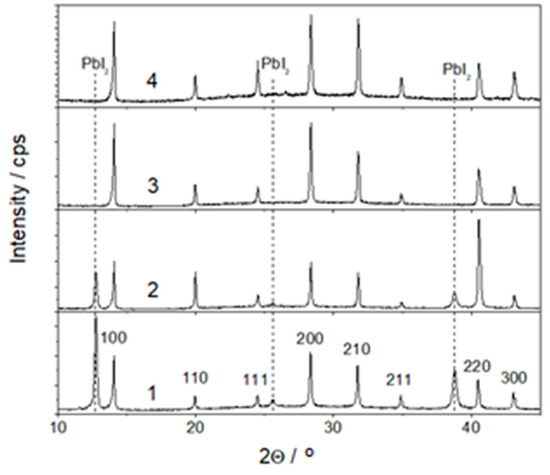
Figure 2.
XRD patterns of perovskite layers with different content of Cs: 1—without Cs, 2—with 5, 3—with 10, 4—with 15% of Cs. The indexed peaks correspond to the perovskite phase FA1/6MA5/6PbBr0.5I2.5.

Table 1.
Values of the lattice parameter a and crystalite size D determined by the XRD.
The most ordered perovskite structure (the largest crystallites are ~61.1 nm) is formed in the solution with 10% of Cs, while the most disordered structure is typical of the sample without Cs. The unit cell volume of the perovskite containing no Cs is equal to a3 = 249.9 Å3, and, according to [45], this value corresponds to the perovskite of composition FA1/6MA5/6PbBr0.5I2.5.
The lattice parameter a weakly correlates with the content of Cs: it is lower by approximately the same value, ~0.01 Å, for all the samples containing Cs in comparison to that without Cs. Most likely, the contraction of the perovskite lattice a was caused by the replacement of organic MA+ (CH3NH3+) (ionic radius 1.8 Å) cations by those of Cs+ (ionic radius 1.74 Å). The peaks at 2Θ angles of 12.4°, 25.5° and 39° (Figure 2) should be attributed to the PbI2 phase (ICDD card 00-007-0235). It is seen that increase in Cs concentration leads to a quite steep decrease in intensity of the PbI2 peaks, and these become undetectable in the samples with 10 and 15% of Cs (patterns 3 and 4 in Figure 2).
Top SEM images of the morphology of the perovskite layers without and with Cs are shown in Figure 3. Presence of PbI2 phase is confirmed by the examination of the images. As cases a and b of Figure 3 show, the surface of the layers formed without and with 5% of Cs is decorated by the bright grains which are attributed to an individual PbI2 phase. Their size and quantity on the surface decrease with a higher content of Cs: considerably smaller and less bright grains of the PbI2 phase are identified in the perovskite containing 10% of Cs (Figure 3c). The PbI2 crystallites become undetectable at the highest, 15%, Cs concentration (Figure 3d). SEM observation of the perovskites allows concluding that Cs-containing samples can be characterized by a less rough surface as compared with the Cs-free ones. The smoothest morphology was observed of the layer formed with 15% CsI (Figure 3d).
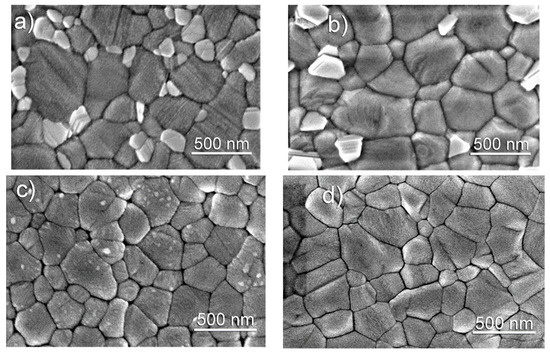
Figure 3.
Top-view SEM images of formed perovskite layers with (a) 0; (b) 5; (c) 10; and (d) 15 % of Cs. Magnification is 100,000×.
The cross-sectional SEM images of the same perovskite cells are shown in Figure 4. It is visible that the thickness of all the examined samples is quite similar: the total thickness of the TiO2 layer (both compact and mesoporous) varies from 150 to 200 nm, and that of the perovskite one is in the range of 550 to 600 nm. It is also worth noting that the perovskite grains with 0 and 5% Cs (Figure 4a,b) seem to be more integral throughout the layer. In the case of perovskite layers containing 10 and 15% Cs, the grains tend to grow on the top of each other (Figure 4c,d).
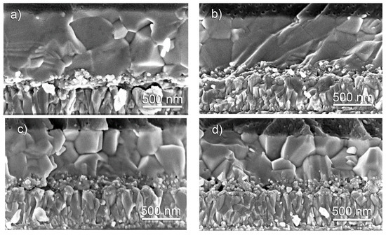
Figure 4.
Cross-sectional SEM images of perovskite cells formed on fluorine-doped tin oxide (FTO) substrate with (a) 0, (b) 5, (c) 10, and (d) 15 % Cs. Magnification is 800,000×.
Influence of cesium concentration on optical transmittance of the layers was investigated with the intention to evaluate their possible utility for the fabrication of monolithic perovskite/silicon tandem solar cells. The measured transmittance spectra of the perovskite layers are depicted in Figure 5. It can be seen that the transparency of the layers in the infrared range decreases slightly with the addition of cesium. All the layers show transmittance higher than 0.55 at 997 nm wavelength, thus indicating relatively low optical loss in the spectral region relevant to the silicon forbidden energy gap.
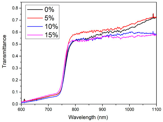
Figure 5.
Optical transmittance spectra of the perovskite layers with a different percentage of cesium.
The measured current–voltage characteristics of the best produced perovskite solar cells with different cesium concentration are shown in Figure 6. It is visible that the open circuit voltage Voc decreases slightly with the addition of cesium, while the short circuit current Jsc first increases with cesium concentration and later drops down. The highest value of the short-current density Jsc demonstrates a solar cell with 10% of Cs concentration.
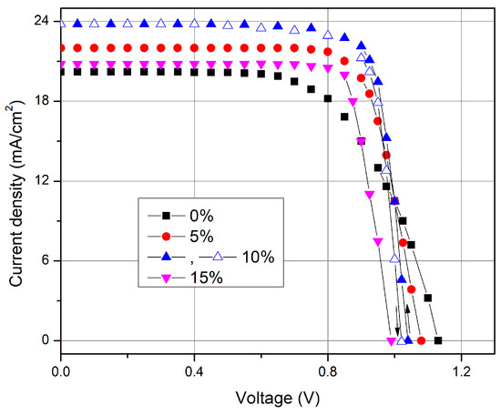
Figure 6.
Current voltage characteristic of the perovskite solar cell with different cesium concentrations.
Photovoltaic quantities of the perovskite solar cells (open circuit voltage, short-current density, fill factor (FF) and power conversion efficiency) with different cesium concentrations are presented in Table 2. Obviously, the solar cell containing 10% of Cs has the highest value of Jsc, FF and PCE. Figure 6 depicts the current-voltage characteristics of solar cell with 10% of Cs measured in forward and reverse directions (full and open triangles, respectively). It is seen that the hysteresis of the current–voltage characteristics of this solar cell is also negligible, as it was observed previously in [35,43]. It should be noted that higher amount of Cs larger than 10% does not improve the performance of the perovskite solar cell.
Table 2.
Photovoltaic parameters of the perovskite solar cells with different cesium concentration.
The continuous wave photoluminescence spectra of the perovskite layers with different cesium concentration are shown in Figure 7. It is seen that the spectra become blue-shifted as the amount of Cs increases. Peak maxima are 770, 767, 763 and 760 nm, respectively, for 0, 5, 10 and 15% of Cs. The blue-shift of 10 nm agrees well with the results observed in [35]. Analysis of PL spectra shows that each peak consists of two Gaussian peaks (peak center λi and width wi are presented in Table 3). They are related to the band–band and excitonic transitions.
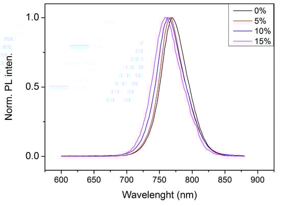
Figure 7.
Photoluminescence spectra of the perovskite layers with different cesium concentration.
Table 3.
Results of PL analysis: λi is peak center and wi is full width at half maximum of the Gaussian peaks, λmax is the peak maximum, τi and Ai are the decay time and the amplitude of the three-exponential function, and τav is the amplitude weighted average decay time.
The time-resolved PL decay curves were measured in the center of the PL peak (see Figure 8). The transients have been approximated using different models like stretched exponential (or Kohlrausch) and compressed hyperbola (or Becquerel) functions [46] or two exponential model, but neither of them provided as good fitting results as the triple exponential approximation (the adjusted R-squared was 0.98 or higher):
with the corresponding intensity amplitudes , and the amplitude weighted average decay times were calculated as
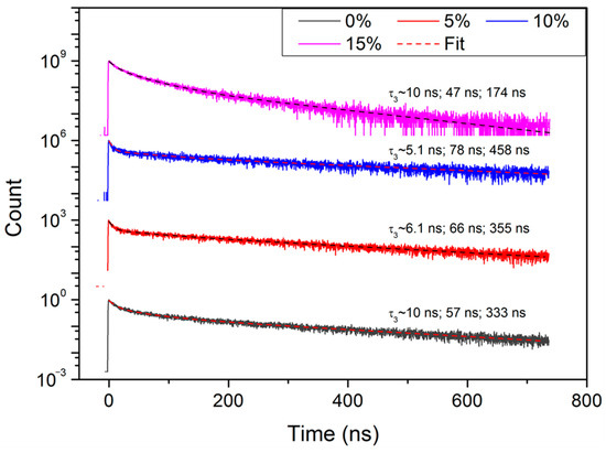
Figure 8.
Photoluminescence decay transients of the perovskite layers with a different cesium concentration.
The deduced decay times and amplitudes are presented in Table 3.
Three decay times are assigned to different recombination mechanisms, thus, two of them are related to band–band and excitonic transitions. Meanwhile, the third decay time could be related to various nonradiative processes.
As can be seen from Table 3, the average decay time increases with the growth of Cs concentration in the range 0 < x ≤ 0.1, and it drops down sharply in the perovskite layer with highest Cs concentration (x = 0.15). The variation of the average decay time with cesium concentration in the perovskite layer correlates well with PCE values of the perovskite solar cells (see Table 2). According to [47], the higher PCE percentage and longer PL decay times are stipulated by lower trap density in perovskite layers containing Cs, as compared to ones without cesium. Lower trap density reduces the nonradiative recombination losses which works in favor of the higher performance of solar cells [42,48].
Small amounts of Cs-cation can be used to influence the perovskite crystal structure by reaching a lower effective tolerance factor leading to a cubic or pseudo-cubic perovskite structure [41,49]. This way, entropic stabilization leads to the desired photo-active phase obtained at room temperature [50]. Cesium can effectively suppress the yellow phase formation of FAPbI3, thus providing with improved and defect-free perovskite thin-films demonstrating stabilized power conversion efficiencies exceeding 21% for up to 1000 h [35]. The triple-cation perovskite is thermally more stable as compared to the FA/MA perovskite and is also more robust against ambient variations such as different preparation protocols, temperatures, and solvent vapors [41]. Singh and Miyasaki [43] confirmed this remarkable stability (up to 18 weeks) of triple-cation perovskites fabricated under environmental conditions with a relative humidity of 25% showing a stabilized PCE exceeding 25%. At a higher concentration (x > 0.1), cesium reduces the performance of the perovskite solar cell. It can be caused by a reduction in the size of the crystallites for perovskite with a Cs concentration larger than 10% (see Table 1) which induced the growth of carrier recombination rate.
4. Conclusions
Experimental study of structure, photoluminescence and optical properties of perovskite Csx(MA0.17FA0.83)(1−x)Pb(I0.83Br0.17)3 layers with different cesium concentration was carried out. It is established that addition of cesium almost does not influence the transparency of the perovskite layers in the infrared range but significantly improves the photovoltaic performance of the perovskite solar cells. It was found that the solar cell with 10% of cesium in the perovskite layer demonstrates the best power conversion efficiency of 20%, and therefore such layers can find application as suitable tandem partners for silicon solar cells.
Author Contributions
Conceptualization and methodology, S.A., K.L. and J.G.; sample fabrication, A.G., K.P. and A.S. (Algirdas Sužiedėlis); formal analysis, A.S. (Algirdas Selskis) and A.S. (Algirdas Sužiedėlis); experimental investigation, E.Š., K.P., A.Č., A.S. (Algirdas Selskis), R.J. and A.L.; writing—reviewing and editing, S.A., R.J., J.G. and K.L.; visualization, A.S. (Algirdas Selskis) and K.P.; project administration and supervision, S.A. All authors have read and agreed to the published version of the manuscript.
Funding
This research was funded by Research Council of Lithuania, Grant number 01.2.2-LMT-K-718-01-0050).
Institutional Review Board Statement
Not applicable.
Informed Consent Statement
Not applicable.
Data Availability Statement
No new data were created or analyzed in this study. Data sharing is not applicable to this article.
Acknowledgments
The authors gratefully acknowledge R. Sedlickas for reading the text of the manuscript and giving valuable suggestions.
Conflicts of Interest
The authors declare no conflict of interest.
References
- Reynolds, S.; Smirnov, V. Modelling of two-and four-terminal thin-film silicon tandem solar cells. J. Phys. Conf. Ser. 2012, 398, 012006. [Google Scholar] [CrossRef]
- Asadpour, R.; Chavali, R.V.K.; Khan, M.R.; Alam, M.A. Bifacial Si heterojunction-perovskite organic-inorganic tandem to produce highly efficient (η*T ~33%) solar cell. Appl. Phys. Let. 2015, 106, 243902. [Google Scholar] [CrossRef]
- Mailoa, J.P.; Bailie, C.D.; Johlin, E.C.; Hoke, E.T.; Akey, A.J.; Nguyen, W.H.; McGehee, M.D.; Buonassisi, T. A 2-terminal perovskite/silicon multijunction solar cell enabled by a silicon tunnel junction. Appl. Phys. Lett. 2015, 106, 121105. [Google Scholar] [CrossRef]
- Albrecht, S.; Saliba, M.; Baena, J.P.C.; Lang, F.; Kegelmann, L.; Mews, M.; Steier, L.; Abate, A.; Rappich, J.; Korte, L.; et al. Monolithic perovskite/silicon-heterojunction tandem solar cells processed at low temperature. Energy Environ. Sci. 2016, 9, 81–88. [Google Scholar] [CrossRef]
- McMeekin, D.P.; Sadoughi, G.; Rehman, W.; Eperon, G.E.; Saliba, M.; Hörantner, M.T.; Haghighirad, A.; Sakai, N.; Korte, L.; Rech, B.; et al. A mixed-cation lead mixed-halide perovskite absorber for tandem solar cells. Science 2016, 351, 151–155. [Google Scholar] [CrossRef]
- Werner, J.; Weng, C.H.; Walter, A.; Fesquet, L.; Seif, J.P.; De Wolf, S.; Niesen, B.; Ballif, C. Efficient monolithic perovskite/silicon tandem solar cell with cell area > 1 cm2. Phys. Chem. Lett. 2016, 7, 161–166. [Google Scholar] [CrossRef]
- Bush, K.A.; Palmstrom, A.F.; Yu, Z.J.; Boccard, M.; Cheacharoen, R.; Mailoa, J.P.; McMeekin, D.P.; Hote, R.L.Z.; Bailie, C.D.; Leijtens, T.; et al. 23.6%-efficient monolithic perovskite/silicon tandem solar cells with improved stability. Nat. Energy. 2017, 2, 17009. [Google Scholar] [CrossRef]
- Werner, J.; Niesen, B.; Ballif, C. Perovskite/silicon tandem solar cells: Marriage of convenience or true love story?– An overview. Adv. Matter. Interf. 2017, 1700731. [Google Scholar] [CrossRef]
- Zheng, J.; Lau, C.F.J.; Mehrvarz, H.; Ma, F.J.; Jiang, Y.J.; Deng, X.F.; Soeriyadi, A.; Kim, J.; Zhang, M.; Hu, L.; et al. Large area efficient interface layer free monolithic perovskite/homo-junction-silicon tandem solar cell with over 20% efficiency. Energy Environ. Sci. 2018, 11, 2432–2443. [Google Scholar] [CrossRef]
- Chen, B.; Yu, Z.; Liu, K.; Zheng, X.; Liu, Y.; Shi, J.; Spronk, D.; Rudd, P.N.; Holman, Z.; Huang, J. Grain engineering for perovskite/silicon monolithic tandem solar cells with efficiency of 25.4%. Joule 2019, 3, 1–14. [Google Scholar] [CrossRef]
- Köhnen, E.; Jošt, M.; Morales-Vilches, A.B.; Tockhorn, P.; Al-Ashouri, A.; Macco, B.; Kegelmann, L.; Korte, L.; Rech, B.; Schlatmann, R.; et al. Highly efficient monolithic perovskite silicon tandem solar cells: Analyzing the influence of current mismatch on device performance. Sustain. Energy Fuels 2019, 3, 1995–2005. [Google Scholar] [CrossRef]
- Jaysankar, M.; Raul, A.B.L.; Bastos, J.; Burgess, C.; Weitens, C.; Creatore, M.; Aernouts, T.; Kuang, Y.; Gehlhaar, R.; Hadipour, A.; et al. Minimizing voltage loss in wide-bandgap perovskite for tandem solar cells. ACS Energy Lett. 2019, 4, 259–264. [Google Scholar] [CrossRef]
- Shen, H.; Walter, D.; Wu, Y.; Fong, K.C.; Jacobs, D.A.; Duong, T.; Peng, J.; Weber, K.; White, T.P.; Catchpole, K.R. Monolithic perovskite/Si tandem solar cell: Pathways to over 30% efficiency. Adv. Energy Mater. 2019, 1902840. [Google Scholar] [CrossRef]
- Lee, C.; Lee, S.-W.; Bae, S.; Shawky, A.; Devaraj, V.; Anisimov, A.; Kauppinen, E.I.; Oh, J.-W.; Kang, Y.; Kim, D.; et al. Carbon nanotube electrode-based perovskite-silicon tandem solar cells. Sol. RRL 2020, 2000353. [Google Scholar] [CrossRef]
- Duong, T.; Pham, H.; Kho, T.C.; Phang, P.; Fong, K.C.; Yan, D.; Yin, Y.; Peng, J.; Mahmud, M.A.; Gharibzadeh, S.; et al. High efficiency perovskite-silicon tandem solar cells: Effect of surface coating versus bulk incorporation of 2D perovskite. Adv. Energy Mater. 2020, 1903553. [Google Scholar] [CrossRef]
- Kojima, A.; Teshima, K.; Shirai, Y.; Miyasaka, T. Organometal halide perovskites as visible-light sensitizers for photovoltaic cells. J. Am. Chem. Soc. 2009, 131, 6050–6051. [Google Scholar] [CrossRef]
- Kothandaraman, R.K.; Jiang, Y.; Feurer, T.; Tiwari, A.N.; Fu, F. Near-infrared-transparent perovskite solar cells and perovskite-based tandem photovoltaics. Small Methods 2020, 4, 2000395. [Google Scholar] [CrossRef]
- Yoshikawa, K.; Kawasaki, H.; Yoshida, W.; Irie, T.; Konishi, K.; Nakano, K.; Uto, T.; Adachi, D.; Kanematsu, M.; Uzu, H.; et al. Silicon heterojunction solar cell with integrated back contacts for a photoconversion efficiency over 26%. Nat. Energy 2017, 2, 17032. [Google Scholar] [CrossRef]
- Yu, C.; Xu, S.; Yao, J.; Han, S. Recent advances in the new perspectives on crystalline silicon solar cells with carrier-selective passivation contacts. Crystals 2018, 8, 430. [Google Scholar] [CrossRef]
- Polman, A.; Knight, M.; Garnett, E.C.; Ehler, B.; Sinke, W.C. Photovoltaic materials:present efficiencies and future challenges. Science 2016, 352, aad4424-1–aad442-10. [Google Scholar] [CrossRef] [PubMed]
- Ašmontas, S.; Gradauskas, J.; Sužiedėlis, A.; Šilėnas, A.; Širmulis, E.; Vaičikauskas, V.; Vaičiūnas, V.; Žalys, O.; Fedorenko, L.; Bulat, L. Photovoltage formation across GaAs p-n junction under illuminationof intense laser radiation. Opt. Quantum Electron. 2016, 48, 448. [Google Scholar] [CrossRef]
- Ašmontas, S.; Gradauskas, J.; Sužiedėlis, A.; Šilėnas, A.; Širmulis, E.; Švedas, V.; Vaičikauskas, V.; Žalys, O. Hot carrier impact on photovoltage formation in solar cells. Appl. Phys. Let. 2018, 113, 071103. [Google Scholar]
- Gradauskas, J.; Ašmontas, S.; Sužiedėlis, A.; Šilėnas, A.; Vaičikauskas, V.; Čerškus, A.; Širmulis, E.; Žalys, O.; Masalskyi, O. Influence of hot carriers and thermal components on photovoltage formation across p-n junction. Appl. Sci. 2020, 10, 7483. [Google Scholar] [CrossRef]
- Jaysankar, M.; Filipič, M.; Zielenski, B.; Schmager, R.; Song, W.; Qiu, W.; Paetzold, U.W.; Aernouts, T.; Debucquoy, M.; Gehlhaar, R.; et al. Perovskite-silicon tandem solar modules with optimized light harvesting. Energy Environ. Sci. 2018, 11, 1489–1498. [Google Scholar] [CrossRef]
- Charibzadeh, S.; Hossain, I.M.; Fassl, P.; Nejand, B.A.; Abzieher, T.; Schultes, M.; Ahlswede, E.; Jackson, P.; Powalla, M.; Schäfer, S.; et al. 2D/3D heterostructure for semitransporant perovskite solar cell with engineering bandgap enables efficiencies exceeding 25% in four-terminal tandems with silicon and CIGS. Adv. Funct. Mater. 2020, 1909919. [Google Scholar] [CrossRef]
- Yeom, K.M.; Kim, S.U.; Woo, M.Y.; Noh, J.H.; Im, S.H. Recent progress in metal halide perovskite-based tandem solar cell. Adv. Mater. 2002, 2002228. [Google Scholar] [CrossRef]
- Jena, A.K.; Kulkarni, A.; Miyasaka, T. Halide perovskite photovoltaic: Background, status, and future prospects. Chem. Rev. 2019, 3036–3103. [Google Scholar] [CrossRef] [PubMed]
- Noh, H.; Im, S.H.; Heo, T.N.; Mandal, T.N.; Seok, S.I. Chemical management for colorful, efficient, and stable inorganic-organic hybrid nanostructured solar cells. Nano Lett. 2013, 13, 1764. [Google Scholar] [CrossRef]
- Pham, H.D.; Xianqiang, L.; Li, W.; Manzhos, S.; Kyaw, A.K.K.; Sonar, P. Organic interfacial materials for perovskite-based optoelectronic devices. Energy Environ. Sci. 2019, 12, 1177–1209. [Google Scholar] [CrossRef]
- Dong, Q.; Fang, Y.; Shao, Y.; Mulligan, P.; Qiu, J.; Cao, L.; Huang, J. Electron-hole diffusion lengths > 175 µm in solution-grown CH3NH3PbI3 single crystals. Science 2015, 347, 967–969. [Google Scholar] [CrossRef] [PubMed]
- Eperon, G.E.; Hörantner, M.T.; Snaith, H.J. Metal halide perovskite tandem and multiple-junction photovoltaics. Nat. Rev. Chem. 2017, 1, 0095. [Google Scholar] [CrossRef]
- Leijtens, T.; Bush, K.A.; Prasanna, R.; McGehe, M.D. Opportunities and challenges for tandem solar cells using metal halide perovskite semiconductors. Nat. Energy. 2018, 3, 828–838. [Google Scholar] [CrossRef]
- Song, Z.; Chen, C.; Li, C.; Awni, R.A.; Zhao, D.; Yan, Y. Wide-gap, low-bandgap, and tandem perovskite solar cells. Semicond. Sci. Technol. 2019, 34, 093001. [Google Scholar] [CrossRef]
- Unger, E.L.; Kegelmann, L.; Suchan, K.; Sorell, D.; Korte, L.; Albrecht, S. Roadmap and roadblocks for the band gap tunability of metal halide perovskite. J. Mater. Chem. A 2017, 5, 11401–11409. [Google Scholar] [CrossRef]
- Saliba, M.; Matsui, T.; Seo, J.Y.; Domaski, K.; Correa-Baena, J.P.; Nazeeruddin, M.K.; Zakeeruddin, S.M.; Tress, W.; Abate, A.; Hagfeldt, A.; et al. Cesium-containing triple cation perovskite solar cells: Improved stability, reproducibility and high efficiency. Energy Environ. Sci. 2016, 9, 1989–1997. [Google Scholar] [CrossRef]
- Correa-Baena, J.P.; Saliba, M.; Buonnassisi, T.; Grätzel, M.; Abate, A.; Tress, W.; Hagfeldt, A. Promises and challenges of perovskite solar cells. Science 2017, 739–744. [Google Scholar] [CrossRef] [PubMed]
- Christians, J.A.; Schulz, P.; Tinkham, J.S.; Schloemer, T.T.; Harvey, S.P.; Tremolet de Villers, B.J.; Sellinger, A.; Berry, J.J.; Luther, J.M. Tailored interfacesof uncapsulated perovskite solar cells > 1000 h operational stability. Nat. Energy. 2018, 3, 68–74. [Google Scholar] [CrossRef]
- Shen, H.; Omelchenko, S.T.; Jacobs, D.A.; Yalamanchili, S.; Wan, Y.; Yan, D.; Phang, P.; Duong, T.; Wu, Y.; Yin, Y.; et al. In situ recombination junction between p-Si and TiO2 enables high-efficiency monolithic perovskite/Si tandem cells. Sci. Adv. 2018, 4, eaau9711. [Google Scholar] [CrossRef] [PubMed]
- Mateen, M.; Arain, Z.; Liu, X.; Yang, Y.; Ding, Y.; Ma, S.; Ren, Y.; Wu, Y.; Tao, Y.; Shi, P. High-performance mixed-cation mixed-halide perovskite solar cells enabled by a facile intermediate technique. J. Power Sources 2020, 448, 227386. [Google Scholar] [CrossRef]
- Liu, P.; Liu, Z.; Qin, C.; He, T.; Li, B.; Ma, L.; Shaheen, K.; Yang, K.; Yang, H.; Liu, H.; et al. High-performance perovskite solar cells based on passivating interfacial and intergranular defects. Sol. Energy Mater. Sol. Cells. 2020, 212, 110555. [Google Scholar] [CrossRef]
- Ünlü, F.; Jung, E.; Haddad, J.; Kulkarni, A.; Öz, S.; Choi, H.; Fischer, T.; Chakraborty, S.; Kirchartz, T.; Mathur, S. Understanding the interplay of stability and efficiency in A-site engineered lead halide perovskite. APL Mater. 2020, 8, 070901. [Google Scholar] [CrossRef]
- Hu, Y.; Hutter, E.M.; Rieder, P.; Grill, I.; Hanisch, J.; Aygüler, M.F.; Hufnagel, A.G.; Handloser, M.; Bein, T.; Hartschun, A.; et al. Understading the role of cesium and rubidium additives in perovskite solar cells: Trap states, charge transport, and recombination. Adv. Energy Mater. 2018, 1703057. [Google Scholar] [CrossRef]
- Singh, T.; Miyasaka, T. Stabilizing the efficiency beyond 20% with the mixed cation perovskite solar cell fabricated in ambient air under controlled humidity. Adv. Energy Mater. 2018, 8, 1700677. [Google Scholar] [CrossRef]
- Domanski, K.; Alharbi, E.A.; Hagfeldt, A.; Grätzel, M.; Tress, W. Systematic investigation of the impact of operation conditions on the degradation behaviour of perovskite solar cells. Nat. Energy 2018, 3, 61–67. [Google Scholar] [CrossRef]
- Jacobsson, J.T.; Baena, J.P.C.; Pazoki, M.; Saliba, M.; Schenk, K.; Grätzel, M.; Hagfeldt, A. An exploration of the compositional space for mixed lead halogen perovskites for high efficiency solar cells. Available online: https://pubs.rsc.org/en/content/getauthorversionpdf/C6EE00030D (accessed on 18 February 2021).
- Berberan-Santos, N.M. A luminescence decay function encompassing the stretched exponential and the compressed hyperbola. Chem. Phys. Lett. 2008, 460, 146–150. [Google Scholar] [CrossRef][Green Version]
- Solanki, A.; Yadav, P.; Turren-Cruz, S.H.; Lim, S.S.; Saliba, M.; Sum, T.C. Cation influence on carrier dynamics in perovskite solar cells. Nano Energy 2019, 58, 604–611. [Google Scholar] [CrossRef]
- Sutton, R.J.; Eperon, G.E.; Miranda, L.; Parrott, E.S.; Kamino, B.A.; Patel, J.B.; Hörantner, M.T.; Johnston, M.B.; Haghighirad, A.A.; Moore, D.T.; et al. Bandgap-tunable lead halide perovskite with high thermal stability for efficient solar cells. Adv. Energy Mater. 2016, 6, 1502458. [Google Scholar] [CrossRef]
- Wu, C.; Guo, D.; Li, P.; Wang, S.; Liu, A.; Wu, F. A study on the effects of mixed organic cations on the structure and properties in lead halide perovskites. Phys. Chem. Chem. Phys. 2020, 22, 3105–3111. [Google Scholar] [CrossRef]
- Yi, C.; Luo, J.; Meloni, S.; Boziki, A.; Ashari-Astani, N.; Grätzel, C.; Zakeeruddin, M.; Röthlisberger, U.; Grätzel, M. Entropic stabilization of mixed A-cation ABX3 metal halide perovskites for high performance perovskite solar cells. Energy Environ. Sci. 2016, 9, 656–662. [Google Scholar] [CrossRef]
Publisher’s Note: MDPI stays neutral with regard to jurisdictional claims in published maps and institutional affiliations. |
© 2021 by the authors. Licensee MDPI, Basel, Switzerland. This article is an open access article distributed under the terms and conditions of the Creative Commons Attribution (CC BY) license (http://creativecommons.org/licenses/by/4.0/).