Article

Direct-ARPES and STM Investigation of FeSe Thin Film Growth by Nd:YAG Laser

1
CNR-IOM, TASC Laboratory in Area Science Park, 34139 Trieste, Italy
2
International Centre for Theoretical Physics (ICTP), 34100 Trieste, Italy
3
Department of Physics, University of Milano, 20133 Milano, Italy
4
Institute of Semiconductors and Solid-State Physics, Johannes Kepler University, 69 Altenbergerstrasse, 4040 Linz, Austria
5
CNR-SPIN, UOS Salerno, 84084 Fisciano (SA), Italy
*
Authors to whom correspondence should be addressed.
Coatings 2021, 11(3), 276; https://doi.org/10.3390/coatings11030276
Submission received: 4 February 2021 / Revised: 17 February 2021 / Accepted: 22 February 2021 / Published: 26 February 2021

Abstract

:
Research on ultrathin quantum materials requires full control of the growth and surface quality of the specimens in order to perform experiments on their atomic structure and electron states leading to ultimate analysis of their intrinsic properties. We report results on epitaxial FeSe thin films grown by pulsed laser deposition (PLD) on CaF 2 (001) substrates as obtained by exploiting the advantages of an all-in-situ ultra-high vacuum (UHV) laboratory allowing for direct high-resolution surface analysis by scanning tunnelling microscopy (STM), synchrotron radiation X-ray photoelectron spectroscopy (XPS) and angle-resolved photoemission spectroscopy (ARPES) on fresh surfaces. FeSe PLD growth protocols were fine-tuned by optimizing target-to-substrate distance d and ablation frequency, atomically flat terraces with unit-cell step heights are obtained, overcoming the spiral morphology often observed by others. In-situ ARPES with linearly polarized horizontal and vertical radiation shows hole-like and electron-like pockets at the Γ and M points of the Fermi surface, consistent with previous observations on cleaved single crystal surfaces. The control achieved in growing quantum materials with volatile elements such as Se by in-situ PLD makes it possible to address the fine analysis of the surfaces by in-situ ARPES and XPS. The study opens wide avenues for the PLD based heterostructures as work-bench for the understanding of proximity-driven effects and for the development of prospective devices based on combinations of quantum materials.

1. Introduction

Quantum materials under confined geometries, such as in ultrathin films host emergent physical phenomena induced by, e.g., the epitaxial stress imposed by the underlying substrate or arising at the interface with other material systems [1,2,3,4]. Much interest is currently devoted to iron selenide (FeSe) that is a member of the ’11 family’ of Fe-based superconductors [4]. FeSe has a simple quasi-two-dimensional crystal structure (i.e., Fe layer sandwiched between two adjacent Se layers), belongs to P4/nmm space group and undergoes a structural phase transition from tetragonal to orthorhombic at ∼90 K [5]. For 100 K < T < 300 K, a nematic state—electronic order that breaks the rotational symmetries without changing the translational symmetry of the lattice, has been observed [6,7]. Interestingly, at low temperatures, FeSe becomes superconducting with a bulk T c   8 K which can raise to 35 K under hydrostatic pressure [8]. Even though several reports on FeSe thin films indicate that the variation of Tc from ∼4 K to ∼100 K is related to epitaxial strain and film thickness [9,10,11,12,13,14,15,16,17,18], the significant T c   70 K measured in a single atomic layer of FeSe film deposited on a SrTiO 3 (001) substrate [14] was associated with interfacial coupling. It is thus necessary to have access to high-quality single-crystalline FeSe ultrathin film specimens for fine analysis studies as well as to explore potential electronic applications in quantum devices.
In order to distinguish between the effect of interfacial coupling with other functional materials (e.g., SrTiO 3 ) from purely substrate-induced strain mechanisms, it is necessary to adopt flexible thin film deposition techniques which allow the growth of a large variety of quantum materials within the same growth system, as well as to perform advanced in-situ characterization of the grown surfaces. In this respect, although molecular beam epitaxy (MBE) has been widely used to obtain very high quality FeSe thin and ultrathin films [19,20], severe limitations arise if heterostructures need to be grown due to compatibility issues generated by the presence of diverse materials within the same deposition system. On the other hand, Pulsed Laser Deposition (PLD) has superior tunability of the growth rate along with the flexibility to grow in-situ multiple heterostructures, and adequate control of volatile elements [21,22]. Progress has also been made in the growth of chalcogenides and superconducting thin films by atomic layer deposition (ALD) technique [23,24].
Here, we report a study of epitaxial FeSe thin films as grown on (001)-oriented CaF 2 single crystal substrates [25,26] using PLD and in-situ high precision characterization of atomic order, stoichiometry, electron states and Fermi surface. The information gained from ex-situ X-ray diffraction (XRD) and X-ray reflectivity (XRR) has allowed refining the growth protocol of FeSe films in single-phase with four-fold symmetry and with a well-defined epitaxial relationship with the substrate. The in-situ analysis by scanning tunneling microscopy (STM) has revealed either screw-type spirals on the samples surface or step flow growth depending on the deposition parameters, and ultimately confirming the growth of continuous layers without voids at the surface. The stoichiometry of the films was confirmed by in-situ core level synchrotron radiation photoemission spectroscopy (XPS) while the polarization-dependent in-situ ARPES allowed to analyse the electronic band structure and Fermi surfaces of the specimens down to the ultrathin limit. The results open wide perspectives for the realization of planar devices based on PLD multi-layered heterostructures as work-bench for the understanding and control of quantum materials and their combinations.

2. Materials and Methods

Epitaxial FeSe thin films were grown on 001-oriented CaF 2 single crystal substrates by PLD technique using an Nd:YAG laser source of 1064 nm wavelength (fundamental harmonics) at the all-in-situ NFFA facility at Trieste (Italy) that also integrates the APE beamlines of IOM-CNR at the Elettra synchrotron radiation source, STM and low energy electron diffraction (LEED) [27,28]. The laser energy density, pulse width and the spot size is 4–5 J-cm 2 , 6 ns, and 2 mm in diameter, respectively. Ablation of a high-purity commercial stoichiometric FeSe target was used for the films’ growth. The as-received substrates were rinsed, sonicated in ethanol and subsequently dried under N 2 atmosphere. During the deposition process, the substrate temperature was kept at 420 ° C and the target-to-substrate distance d was varied between 6.8 and 7.5 cm for optimizing growth kinetics. The FeSe films were deposited at background pressures of 10 8 –10 7 mbar with different laser repetition rates (1–0.1 Hz). The structural and thickness characterizations were performed ex-situ by means of PANalytical X’Pert four-circle XRD and X-Ray reflectivity (XRR). The film stoichiometry was probed by energy dispersive spectroscopy (EDS) and electrical transport measurements were performed by standard four-probe Van der Pauw technique. The surface topography of the freshly grown films was probed in-situ by STM [29]. Ultraviolet to soft X-ray radiation photoemission spectroscopy (ARPES and XPS) experiments were carried out exploiting the beam characteristics of both APE beamlines receiving variable polarization radiation from dedicated APPLE-II undulator sources of the Elettra storage ring. XPS spectra were acquired by using horizontally polarized light with photon excitation energy of 900 eV and with the Omicron E125 hemispherical electron energy analyzer. ARPES spectra were acquired with linearly polarized (vertical and horizontal) light using a Scienta DA30 hemispherical analyser operated in deflection mode [30].

3. Results

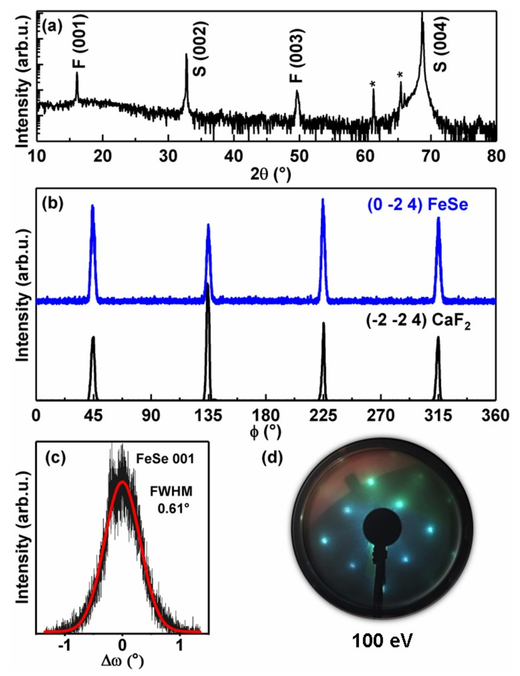
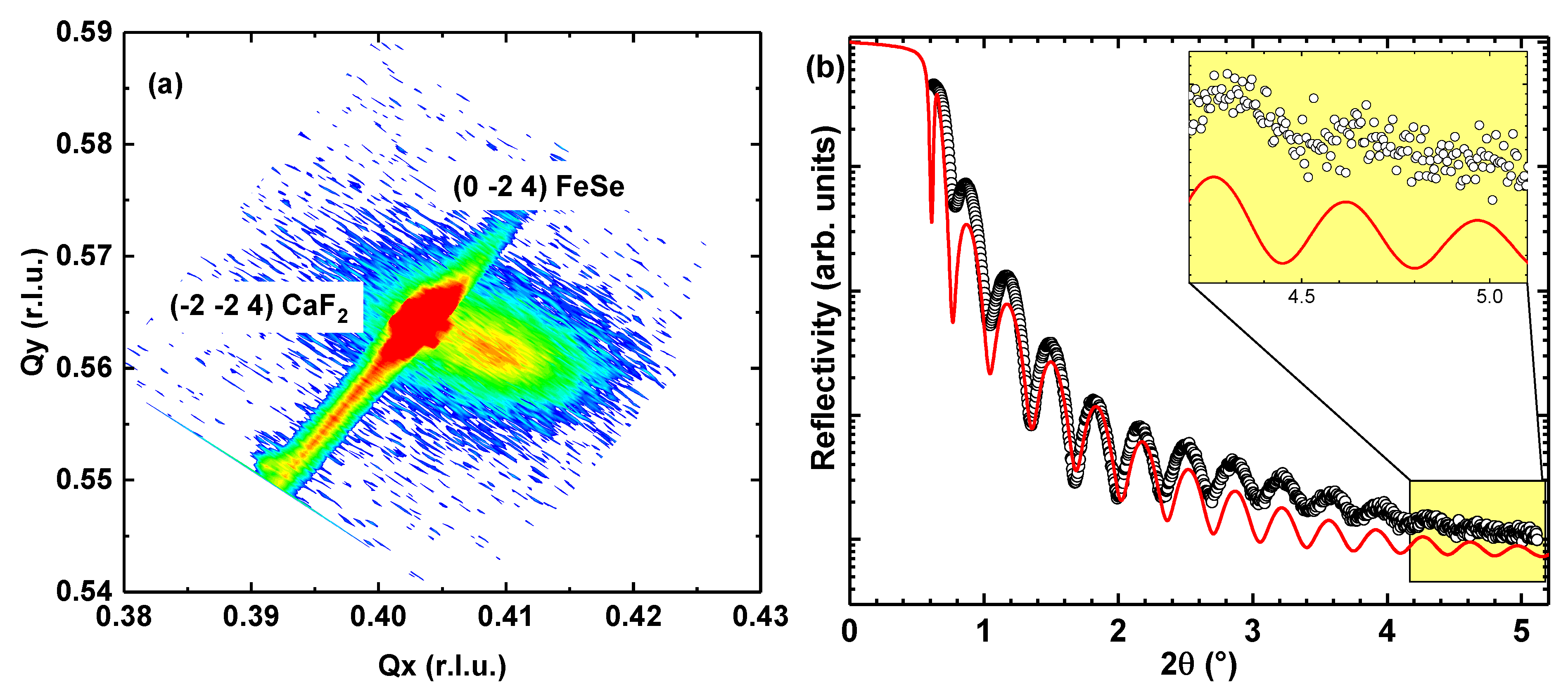
3.1. Structural Properties

Figure 1a shows the long-range θ –2 θ symmetrical XRD scan of a FeSe films grown on a CaF 2 (001) substrate. The FeSe films have a (00l) orientation, pointing a preferential growth direction along the c-axis. The (002) and (004) peaks of FeSe are almost superimposed within those of the substrate peaks. The out-of-plane lattice parameter c calculated from the (001) peak of FeSe is ≈0.551 nm, in agreement with the values reported for an unstrained film [9]. The in-plane epitaxial relationship between the FeSe film and the CaF 2 (001) substrate is determined by the XRD ϕ scans around (−2 −2 4) CaF 2 and (0 −2 4) FeSe asymmetric peak reflections, as shown in Figure 1b. The peaks for both the substrate and film are separated by 90 ° demonstrating a four-fold symmetry, with the (100) plane of the FeSe film aligned parallel to the (110) plane of the substrate [4,31]. As a result of the optimal lattice matching between the diagonal of CaF 2 with the in-plane lattice parameter of FeSe, the film grows with an in-plane rotation of 45 ° with respect to the substrate. The full-width half maxima (FWHM) obtained for the FeSe (001) rocking curves is 0.61 ° (Figure 1c), similar to the FWHM reported in the literature [31]. The surface long-range order was probed in-situ by LEED on a freshly grown FeSe film, shown in Figure 1d. The LEED pattern acquired at 100 eV incident electron energy displays sharp diffraction spots with four-fold symmetry square lattice rotated by 45 ° , i.e., along the substrate surface cell diagonal.
Figure 2a shows the reciprocal space maps (RSM) performed around the asymmetric Bragg reflections of (−2 −2 4) CaF 2 and (0 −2 4) FeSe film. The diffraction intensities of the film and substrate do not align along the same in-plane scattering vector Q x , confirming that the film is relaxed. The film thickness measured by XRR of approximately 45 uc, is shown in Figure 2b. Numerical simulations of the low-angle XRR data (i.e., solid curve in Figure 2b) are performed using the IMD package of the XOP software [32]. XRR oscillations can be seen for 2 θ values up to 5 degrees and above it, the oscillations fall below the experimental sensitivity of the x-ray diffractometer [33,34]. The estimated growth rate of the film is ≈0.13 Å per laser pulse. Temperature-dependent electrical transport measurements show metallic nature (not shown here) with room-temperature resistivity of ≈700 μ Ω -cm. The calculated residual resistivity ratio (R 300 K /R 20 K ) is ≈2.15 for the film on CaF 2 substrate, estimating that the T c of the films considered here lies below 3 K.

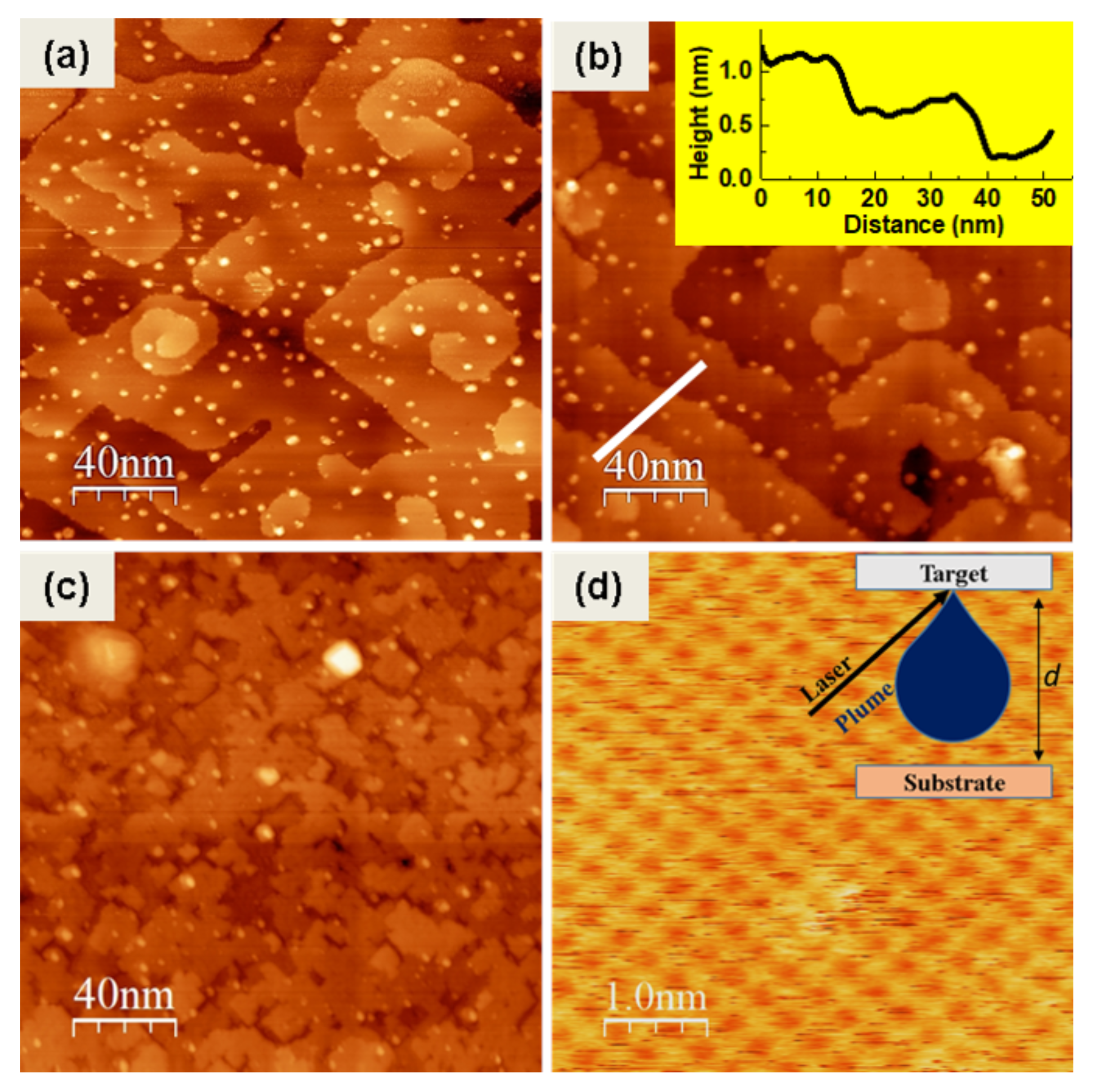
3.2. Scanning Tunneling Microscopy

To determine the surface topography and surface roughness of the films, in-situ room temperature STM measurements were performed [29]. Inset of Figure 3d shows the schematic of the PLD system depicted with the target-to-substrate distance d used as control parameter for tuning and optimizing the growth kinetics. Figure 3a shows the STM topography image of 28-uc FeSe film in the scan area (200 × 200) nm 2 as deposited at 1Hz laser frequency and target-to-substrate distance d   6.8 cm. The surface topography reveals atomically flat terraces and uniformly distributed dot-like features. Moreover, the STM image in Figure 3a confirms the onset of screw-type growth mode. In order to minimize the density of dot-like features on the film surface, d has been progressively increased from 6.8 to 7.5 cm over the sample’s series. As d is increased, the growth rate of the film decreases [35]. The reduction in growth rate favors the uniform arrangement of the ablated incoming species, until the step flow growth regime is stabilized. A STM topography for a 28-uc FeSe film grown at 0.1 Hz and d 7.5 cm is shown in Figure 3b, displaying uniform step flow growth and over 70% reduction in the density of dot-like features. The calculated root mean square (RMS) roughness of the 28-uc FeSe layer is ∼0.35 nm. Inset of Figure 3b shows the line profile along the solid line indicating the step height of ∼0.56 nm, i.e., equivalent to the height of one FeSe unit cell. When reducing the thickness of the FeSe film from 28 uc to 1.5-uc, the step flow growth is maintained and the layers are continuous as shown in Figure 3c. This indicates that our PLD grown films are uniform over the whole substrate surface. Compared to typical PLD growth parameters (i.e., d ∼ 4–5 cm, laser frequency of 3–10 Hz) [31,36], here, we have dramatically increased the d to 7.5 cm (i.e., about a 70%–80% increment) and reduced the laser frequency to 0.1 Hz (i.e., 1 laser pulse for every 10 s) for the growth of FeSe films. Such extreme fine-tuning is essential for achieving atomically-flat FeSe surfaces by the 1st harmonic Nd:YAG laser. The high quality of the resulting films is also confirmed by atomic-resolution STM topography of FeSe film in the scan area of (5 × 5) nm 2 reproduced in Figure 3d [37].

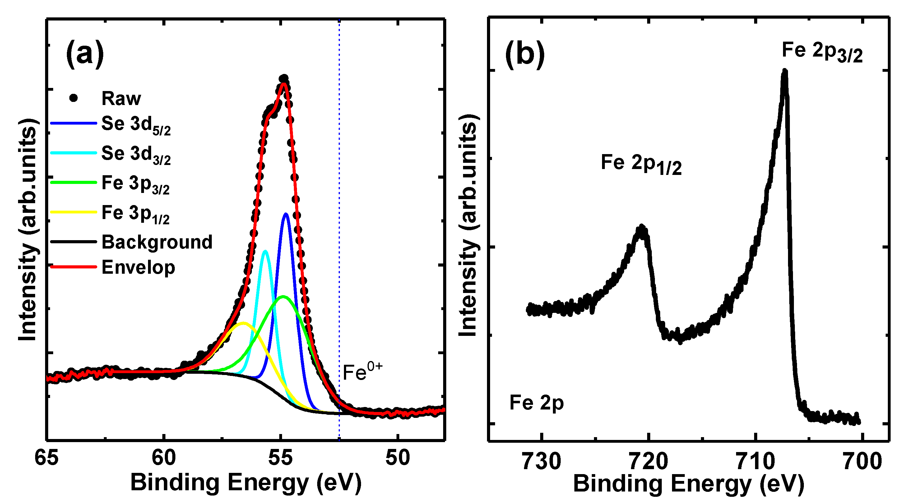
3.3. X-Ray Photoemission Spectroscopy

The core-level XPS spectra of the Fe 2p and Se 3d of the FeSe films measured in-situ by transferring the films to the APE-HE beamline end-station, are shown in Figure 4. The XPS spectra were recorded with the sample surface oriented at 45 ° with respect to the incident photon radiation. The energy interval considered in Figure 4a covers the binding energy range including both the Se 3d and Fe 2p core levels. The photoemission spectrum shows different components and a numerical de-convolution made after subtracting a Shirley background, and by using mixed Gaussian-Lorentzian line shapes constrained by the spin-orbit splitting and statistical intensity ratios. It is found that the Se 3d spin-orbit split components 3d 5 / 2 and 3d 3 / 2 are located at 54.8 and 55.65 eV binding energies, while the contribution from Fe 3p is located at 54.9 and 56.6 eV [38,39]. Fe 2p XPS core-level spectra with metallic Donjiac-Sunjic broadening is shown in Figure 4b with the expected spin-orbit and intensity ratio are fully consistent with earlier reports on FeSe and FeTe films [40].

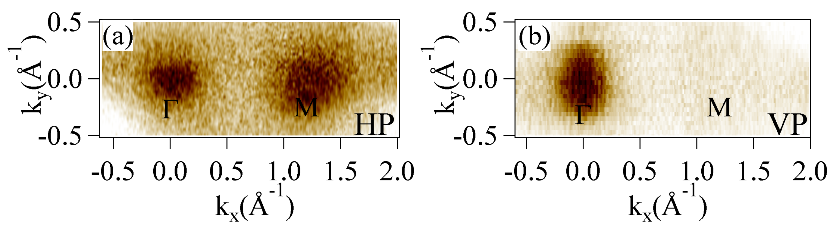
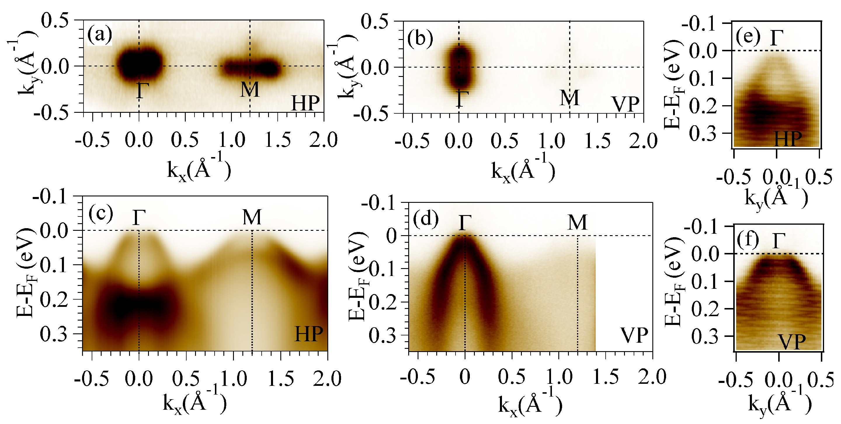
3.4. Angle Resolved Photoemission Spectroscopy

The electronic band structure of the FeSe films was probed by ARPES at the APE-LE end station [30]. The measurements were carried out at 45 K using both horizontally and vertically polarized light of h ν = 85 eV. Horizontal/vertical polarization (HP/VP) directions were parallel/orthogonal to the plane of the synchrotron orbit, and the light incidence angle at normal emission was 45 ° with respect to the sample surface normal. In this configuration, the VP vector lies fully in the sample plane, while the HP has both in-plane and out-of-plane components. Therefore, while VP may probe the states primarily originating from in-plane orbital contributions, HP is sensitive to the states originating from both in-plane and out-of-plane orbitals. In the experiment considered here, the Γ -M high-symmetry direction was aligned parallel to the analyzer slit, which is also perpendicular to the plane of the synchrotron orbit, i.e., parallel to the VP vector.
Here, we are showing as an example on how the topography of the FeSe film surface changes its electronic states while probing with ARPES. When the growth mode of the film is screw-type with droplets present on the film surface (Figure 3a), the Fermi surface maps probed by arpes using HP (Figure 5a) and VP (Figure 5b) shows very broad with no distinct features observable either at Γ or at M-point, respectively. Therefore, we have progressively increased the d to minimize the droplets and maintain step-flow growth mode, and to obtain sharp bands as discussed below.
Figure 6a,b show the Fermi surfaces measured with HP and VP, respectively, for the 28 uc FeSe film grown on CaF 2 substrate. In Figure 6a an ellipse with the major axis oriented along k x is centered at the Γ -point, and around the M-point, a horizontally (vertically) located intense (weak) bone-shaped states are observed. An ellipse centered at the Γ point detected with VP has its major axis along k y (Figure 6b), and 4 lobes of weak equal intensity are observed at the M point. The horizontal and vertical cuts of Figure 6a measured along the Γ -M high symmetry direction using HP light are shown in Figure 6c,e, respectively. A hole-like band with different k F in each cut is detected at the Γ -point. The band at Γ in the vertical cut (Figure 6e) is sharper than the band in the horizontal cut (Figure 6c). This difference results in the elliptical shape of the photoemission distribution observed in the Fermi surface (Figure 6a). By changing the polarization to vertical (Figure 6d,f), we observed that the 2 cuts were exchanged. That is, the sharper and wider bands at Γ are observed in the horizontal (Figure 6d) and vertical (Figure 6f) cuts, respectively, which rotates the ellipse at the Γ -point in the Fermi surface by 90 ° as seen in Figure 6b [41]. The bands observed in the horizontal cut at the M-point and measured with HP (Figure 6c) correspond to bone-shaped features as seen in the Fermi surface reported in Figure 6a, whereas, no bands were observed when measured at the M-point in VP (Figure 6b,d). Taking into account that the sensitivity to electron band states depends on various factors such as the polarization of light, experimental geometry and the photon excitation energy [42,43] etc, it is concluded that the overall contribution of the bands at the Γ and M points are mostly derived from the Fe t 2 g states. The overall ARPES data from the PLD grown films are consistent with those reported for FeSe crystals and MBE films [8].

4. Conclusions

In summary, we have demonstrated fabrication of very high-quality epitaxial FeSe thin films on CaF 2 (001) substrates by PLD technique and studied their structural, morphological and electronic properties. By tuning the PLD deposition parameters such as target-to-substrate distance d and the laser frequency, the step-flow growth with atomically flat surfaces has been achieved. The band structure observed in ARPES also confirms the excellent surface quality of the films, as the data are compatible with the best ones obtained so far on cleaved FeSe single crystals and MBE films. These findings open wide perspectives for the PLD growth technique which is suitable for in-situ growth of heterostructures, e.g., by combining oxides and/or (topological) chalcogenides and potentially superconducting selenides, enabling to study exotic electronic configurations, such as Majorana fermions, and ultimately to explore proximity-induced effects and interface functionalities potentially relevant for device applications.

Author Contributions

Conceptualization, S.K.C. and P.O.; methodology, S.K.C., D.M., C.B., J.F., R.A., R.C., A.B., G.P., G.R., I.V. and P.O.; validation, S.K.C., D.M., C.B., J.F., R.A., R.C., A.B., G.P., G.R., I.V. and P.O.; formal analysis, S.K.C., D.M., C.B., J.F., G.R., I.V. and P.O.; writing—original draft preparation, S.K.C., G.R. and P.O.; writing—review and editing, S.K.C., D.M., C.B., J.F., R.A., R.C., A.B., G.P., G.R., I.V. and P.O.; All authors have read and agreed to the published version of the manuscript.

Funding

D.M. acknowledges the receipt of a fellowship from the ICTP Programme for Training and Research in Italian Laboratories, Trieste, Italy. R.A. and A.B. acknowledges the support by the Austrian Science Fund (FWF) through Projects No. P26830, No. P31423 and H2020 NFFA-Europe 654360.

Institutional Review Board Statement

Not applicable.

Informed Consent Statement

Not applicable.

Data Availability Statement

The data presented in this study are available on request from the corresponding author.

Acknowledgments

This work has been performed in the framework of the Nanoscience Foundry and Fine Analysis (NFFA-MIUR Italy Progetti Internazionali) facility.

Conflicts of Interest

The authors declare no conflict of interest.

References

  1. Sakoda, M.; Iida, K.; Naito, M. Recent progress in thin-film growth of Fe-based superconductors: Superior superconductivity achieved by thin films. Supercond. Sci. Technol. 2018, 31, 093001. [Google Scholar] [CrossRef]
  2. Ding, H.; Lv, Y.F.; Zhao, K.; Wang, W.L.; Wang, L.; Song, C.L.; Chen, X.; Ma, X.C.; Xue, Q.K. High-temperature superconductivity in single-unit-cell FeSe films on anatase TiO2 (001). Phys. Rev. Lett. 2016, 117, 1–5. [Google Scholar] [CrossRef] [Green Version]
  3. Wang, Q.; Zhang, W.; Zhang, Z.; Sun, Y.; Xing, Y.; Wang, Y.; Wang, L.; Ma, X.; Xue, Q.K.; Wang, J. Thickness dependence of superconductivity and superconductor- insulator transition in ultrathin FeSe films on SrTiO3 (001) substrate. 2D Mater. 2015, 2. [Google Scholar] [CrossRef] [Green Version]
  4. Mele, P. Superconducting properties of iron chalcogenide thin films. Sci. Technol. Adv. Mater. 2012, 13, 054301. [Google Scholar] [CrossRef] [Green Version]
  5. McQueen, T.M.; Williams, A.J.; Stephens, P.W.; Tao, J.; Zhu, Y.; Ksenofontov, V.; Casper, F.; Felser, C.; Cava, R.J. Tetragonal-to-orthorhombic structural phase transition at 90 K in the superconductor Fe1.01Se. Phys. Rev. Lett. 2009, 103, 057002. [Google Scholar] [CrossRef]
  6. Watson, M.D.; Kim, T.K.; Haghighirad, A.A.; Davies, N.R.; McCollam, A.; Narayanan, A.; Blake, S.F.; Chen, Y.L.; Ghannadzadeh, S.; Schofield, A.J.; et al. Emergence of the nematic electronic state in FeSe. Phys. Rev. B 2015, 91, 155106. [Google Scholar] [CrossRef] [Green Version]
  7. Shimojima, T.; Suzuki, Y.; Nakamura, A.; Mitsuishi, N.; Kasahara, S.; Shibauchi, T.; Matsuda, Y.; Ishida, Y.; Shin, S.; Ishizaka, K. Ultrafast nematic-orbital excitation in FeSe. Nat. Commun. 2019, 10, 1–6. [Google Scholar] [CrossRef] [Green Version]
  8. Liu, X.; Zhao, L.; He, S.; He, J.; Liu, D.; Mou, D.; Shen, B.; Hu, Y.; Huang, J.; Zhou, X.J. Electronic structure and superconductivity of FeSe-related superconductors. J. Phys. Condens. Matter 2015, 27, 183201. [Google Scholar] [CrossRef] [Green Version]
  9. Nie, Y.F.; Brahimi, E.; Budnick, J.I.; Hines, W.A.; Jain, M.; Wells, B.O. Suppression of superconductivity in FeSe films under tensile strain. Appl. Phys. Lett. 2009, 94, 95–98. [Google Scholar] [CrossRef] [Green Version]
  10. Liu, D.; Zhang, W.; Mou, D.; He, J.; Ou, Y.B.; Wang, Q.Y.; Li, Z.; Wang, L.; Zhao, L.; He, S.; et al. Electronic origin of high-temperature superconductivity in single-layer FeSe superconductor. Nat. Commun. 2012, 3, 1–6. [Google Scholar] [CrossRef] [PubMed] [Green Version]
  11. Tan, S.; Zhang, Y.; Xia, M.; Ye, Z.; Chen, F.; Xie, X.; Peng, R.; Xu, D.; Fan, Q.; Xu, H.; et al. Interface-induced superconductivity and strain-dependent spin density waves in FeSe/SrTiO3 thin films. Nat. Mater. 2013, 12, 634–640. [Google Scholar] [CrossRef] [PubMed] [Green Version]
  12. He, S.; He, J.; Zhang, W.; Zhao, L.; Liu, D.; Liu, X.; Mou, D.; Ou, Y.B.; Wang, Q.Y.; Li, Z.; et al. Phase diagram and electronic indication of high-temperature superconductivity at 65 K in single-layer FeSe films. Nat. Mater. 2013, 12, 605–610. [Google Scholar] [CrossRef] [PubMed]
  13. Zhang, W.H.; Sun, Y.; Zhang, J.S.; Li, F.S.; Guo, M.H.; Zhao, Y.F.; Zhang, H.M.; Peng, J.P.; Xing, Y.; Wang, H.C.; et al. Direct observation of high-temperature superconductivity in one-unit-cell FeSe films. Chin. Phys. Lett. 2014, 31. [Google Scholar] [CrossRef] [Green Version]
  14. Lee, J.J.; Schmitt, F.T.; Moore, R.G.; Johnston, S.; Cui, Y.T.; Li, W.; Yi, M.; Liu, Z.K.; Hashimoto, M.; Zhang, Y.; et al. Interfacial mode coupling as the origin of the enhancement of Tc in FeSe films on SrTiO3. Nature 2014, 515, 245–248. [Google Scholar] [CrossRef] [PubMed]
  15. Liu, X.; Liu, D.; Zhang, W.; He, J.; Zhao, L.; He, S.; Mou, D.; Li, F.; Tang, C.; Li, Z.; et al. Dichotomy of the electronic structure and superconductivity between single-layer and double-layer FeSe/SrTiO3 films. Nat. Commun. 2014, 5, 5047. [Google Scholar] [CrossRef] [Green Version]
  16. Suzuki, Y.; Shimojima, T.; Sonobe, T.; Nakamura, A.; Sakano, M.; Tsuji, H.; Omachi, J.; Yoshioka, K.; Kuwata-Gonokami, M.; Watashige, T.; et al. Momentum-dependent sign inversion of orbital order in superconducting FeSe. Phys. Rev. B 2015, 92, 205117. [Google Scholar] [CrossRef] [Green Version]
  17. Ge, J.F.; Liu, Z.L.; Liu, C.; Gao, C.L.; Qian, D.; Xue, Q.K.; Liu, Y.; Jia, J.F. Superconductivity above 100 K in single-layer FeSe films on doped SrTiO3. Nat. Mater. 2015, 14, 285–289. [Google Scholar] [CrossRef] [PubMed]
  18. Biswas, P.K.; Salman, Z.; Song, Q.; Peng, R.; Zhang, J.; Shu, L.; Feng, D.L.; Prokscha, T.; Morenzoni, E. Direct evidence of superconductivity and determination of the superfluid density in buried ultrathin FeSe grown on SrTiO3. Phys. Rev. B 2018, 97, 174509. [Google Scholar] [CrossRef] [Green Version]
  19. Shigekawa, K.; Nakayama, K.; Kuno, M.; Phan, G.N.; Owada, K.; Sugawara, K.; Takahashi, T.; Sato, T. Dichotomy of superconductivity between monolayer FeS and FeSe. Proc. Natl. Acad. Sci. USA 2019, 116, 24470–24474. [Google Scholar] [CrossRef] [Green Version]
  20. Wang, Z.; Liu, C.; Liu, Y.; Wang, J. High-temperature superconductivity in one-unit-cell FeSe films. J. Phys. Condens. Matter 2017, 29. [Google Scholar] [CrossRef] [Green Version]
  21. Orgiani, P.; Bigi, C.; Kumar Das, P.; Fujii, J.; Ciancio, R.; Gobaut, B.; Galdi, A.; Sacco, C.; Maritato, L.; Torelli, P.; et al. Structural and electronic properties of Bi2Se3 topological insulator thin films grown by pulsed laser deposition. Appl. Phys. Lett. 2017, 110, 1–6. [Google Scholar] [CrossRef] [Green Version]
  22. Bigi, C.; Orgiani, P.; Nardi, A.; Troglia, A.; Fujii, J.; Panaccione, G.; Vobornik, I.; Rossi, G. Robustness of topological states in Bi2 Se3 thin film grown by Pulsed Laser Deposition on (001)-oriented SrTiO3 perovskite. Appl. Surf. Sci. 2019, 473, 190–193. [Google Scholar] [CrossRef]
  23. Burdastyh, M.V.; Postolova, S.V.; Proslier, T.; Ustavshikov, S.S.; Antonov, A.V.; Vinokur, V.M.; Mironov, A.Y. Superconducting phase transitions in disordered NbTiN films. Sci. Rep. 2020, 10, 1471. [Google Scholar] [CrossRef] [PubMed]
  24. Yoo, C.; Kim, W.; Jeon, J.W.; Park, E.S.; Ha, M.; Lee, Y.K.; Hwang, C.S. Atomic layer deposition of Gex Se1–x thin films for endurable ovonic threshold selectors with a low threshold voltage. ACS Appl. Mater. Interfaces 2020, 12, 23110–23118. [Google Scholar] [CrossRef]
  25. Kurth, F.; Reich, E.; Hänisch, J.; Ichinose, A.; Tsukada, I.; Hühne, R.; Trommler, S.; Engelmann, J.; Schultz, L.; Holzapfel, B.; et al. Versatile fluoride substrates for Fe-based superconducting thin films. Appl. Phys. Lett. 2013, 102. [Google Scholar] [CrossRef]
  26. Qiu, W.; Ma, Z.; Patel, D.; Sang, L.; Cai, C.; Shahriar Al Hossain, M.; Cheng, Z.; Wang, X.; Dou, S.X. The interface structure of FeSe thin film on CaF2 substrate and its influence on the superconducting performance. ACS Appl. Mater. Interfaces 2017, 9, 37446–37453. [Google Scholar] [CrossRef] [PubMed]
  27. Nanoscience Foundries and Fine Analysis. Available online: www.trieste.nffa.eu (accessed on 5 December 2020).
  28. Chaluvadi, S.K.; Mondal, D.; Bigi, C.; Knez, D.; Rajak, P.; Ciancio, R.; Fujii, J.; Panaccione, G.; Vobornik, I.; Rossi, G.; et al. Pulsed laser deposition of thin films by means of Nd:YAG laser source operating at its 1st harmonic: Recent approaches and advances. J. Phys. Mater. 2021. [Google Scholar] [CrossRef]
  29. Panaccione, G.; Vobornik, I.; Fujii, J.; Krizmancic, D.; Annese, E.; Giovanelli, L.; Maccherozzi, F.; Salvador, F.; De Luisa, A.; Benedetti, D.; et al. Advanced photoelectric effect experiment beamline at Elettra: A surface science laboratory coupled with Synchrotron Radiation. Rev. Sci. Instrum. 2009, 80, 043105. [Google Scholar] [CrossRef] [Green Version]
  30. Bigi, C.; Das, P.K.; Benedetti, D.; Salvador, F.; Krizmancic, D.; Sergo, R.; Martin, A.; Panaccione, G.; Rossi, G.; Fujii, J.; et al. Very efficient spin polarization analysis (VESPA): New exchange scattering-based setup for spin-resolved ARPES at APE-NFFA beamline at Elettra. J. Synchrotron Radiat. 2017, 24, 750–756. [Google Scholar] [CrossRef] [Green Version]
  31. Feng, Z.; Yuan, J.; He, G.; Hu, W.; Lin, Z.; Li, D.; Jiang, X.; Huang, Y.; Ni, S.; Li, J.; et al. Tunable critical temperature for superconductivity in FeSe thin films by pulsed laser deposition. Sci. Rep. 2018, 8, 1–6. [Google Scholar] [CrossRef]
  32. Windt, D.L. IMD—Software for modeling the optical properties of multilayer films. Comput. Phys. 1998, 12, 360. [Google Scholar] [CrossRef] [Green Version]
  33. Orgiani, P.; Perucchi, A.; Knez, D.; Ciancio, R.; Bigi, C.; Chaluvadi, S.K.; Fujii, J.; Vobornik, I.; Panaccione, G.; Rossi, G.; et al. Tuning the optical absorption of anatase thin films across the visible-to-near-infrared spectral region. Phys. Rev. Appl. 2020, 13, 044011. [Google Scholar] [CrossRef]
  34. Nardi, A.; Bigi, C.; Kumar Chaluvadi, S.; Ciancio, R.; Fujii, J.; Vobornik, I.; Panaccione, G.; Rossi, G.; Orgiani, P. Analysis of metal-insulator crossover in strained SrRuO3 thin films by X-ray photoelectron spectroscopy. Coatings 2020, 10, 780. [Google Scholar] [CrossRef]
  35. Mostako, A.T.T.; Khare, A. Effect of target–substrate distance onto the nanostructured rhodium thin films via PLD technique. Appl. Nanosci. 2012, 2, 189–193. [Google Scholar] [CrossRef] [Green Version]
  36. Zhuang, J.C.; Yeoh, W.K.; Cui, X.Y.; Kim, J.H.; Shi, D.Q.; Shi, Z.X.; Ringer, S.P.; Wang, X.L.; Dou, S.X. Enhancement of transition temperature in FexSe0.5Te0.5 film via iron vacancies. Appl. Phys. Lett. 2014, 104, 262601. [Google Scholar] [CrossRef] [Green Version]
  37. Song, C.L.; Wang, Y.L.; Cheng, P.; Jiang, Y.P.; Li, W.; Zhang, T.; Li, Z.; He, K.; Wang, L.; Jia, J.F.; et al. Direct observation of nodes and twofold symmetry in FeSe superconductor. Science 2011, 332, 1410–1413. [Google Scholar] [CrossRef] [Green Version]
  38. Cho, J.S.; Park, J.S.; Kang, Y.C. Preparation of Hollow Fe2SO3 Nanorods and Nanospheres by Nanoscale Kirkendall Diffusion, and Their Electrochemical Properties for Use in Lithium-Ion Batteries. Sci. Rep. 2016, 6, 1–13. [Google Scholar] [CrossRef] [PubMed]
  39. Telesca, D.; Nie, Y.; Budnick, J.I.; Wells, B.O.; Sinkovic, B. Impact of valence states on the superconductivity of iron telluride and iron selenide films with incorporated oxygen. Phys. Rev. B 2012, 85, 214517. [Google Scholar] [CrossRef] [Green Version]
  40. Telesca, D.; Nie, Y.; Budnick, J.I.; Wells, B.O.; Sinkovic, B. Surface valence states and stoichiometry of non-superconducting and superconducting FeTe films. Surf. Sci. 2012, 606, 1056–1061. [Google Scholar] [CrossRef]
  41. Zhang, Y.; He, C.; Ye, Z.R.; Jiang, J.; Chen, F.; Xu, M.; Ge, Q.Q.; Xie, B.P.; Wei, J.; Aeschlimann, M.; et al. Symmetry breaking via orbital-dependent reconstruction of electronic structure in detwinned NaFeAs. Phys. Rev. B 2012, 85, 085121. [Google Scholar] [CrossRef] [Green Version]
  42. Damascelli, A. Probing the electronic structure of complex systems by ARPES. Phys. Scr. 2004, T109, 61. [Google Scholar] [CrossRef] [Green Version]
  43. Vobornik, I.; Fujii, J.; Mulazzi, M.; Panaccione, G.; Hochstrasser, M.; Rossi, G. Surface electron bands and Fermi surface of Be(0001). Phys. Rev. B—Condens. Matter Mater. Phys. 2005, 72, 3–8. [Google Scholar] [CrossRef]
Figure 1. (a) θ –2 θ XRD pattern of a FeSe film deposited by PLD on a CaF 2 (001) substrate; The symbols ‘F’, ‘S’, ‘*’ indicate the film, substrate and characteristic x-rays peaks, (b) asymmetric Φ scans along (0 −2 4) of FeSe and (−2 −2 4) of CaF 2 reflections, (c) rocking curve performed around the (001) peak of the FeSe film, (d) LEED pattern of the FeSe film on a CaF 2 (001) substrate measured at 100 eV.
Coatings 11 00276 g001
Figure 2. (a) Asymmetric reciprocal space maps of (0 −2 4) FeSe film and (−2 −2 4) CaF 2 substrate, (b) X-ray reflectivity curve of a FeSe film showing both experimental data (circles) and simulation (solid lines) deposited on CaF 2 (001) substrate.
Coatings 11 00276 g002
Figure 3. STM topography of a FeSe film grown by PLD. 28 uc film deposited at (a) d = 6.8 cm, (b) d = 7.5 cm, respectively. Inset to (b): line profile measured along the solid line in (b). (c) 1.5 uc FeSe deposited at d = 7.5 cm, (d) (5 × 5) nm 2 atomic resolution STM topography of the surface in (a). Inset to (d): Schematic of the PLD system.
Coatings 11 00276 g003
Figure 4. Core-level XPS spectra of (a) Se 3d along with its fitted components (solid lines) and (b) Fe 2p spectra of FeSe films.
Coatings 11 00276 g004
Figure 5. ARPES measurements of a 28-uc FeSe film deposited at d = 6.8 cm on CaF 2 measured with a photon energy of 85 eV at 45 K. ARPES maps measured with (a) HP (b) VP of the light, respectively.
Coatings 11 00276 g005
Figure 6. ARPES measurements of a 28-uc FeSe film deposited at d = 7.5 cm on CaF 2 measured with a photon energy of 85 eV at 45 K. ARPES maps measured with (a) HP (b) VP of the light. (c,d) Horizontal cuts along the Γ -M direction; (e,f) vertical cuts along the Γ direction taken from (a) and (b), respectively.
Coatings 11 00276 g006
Publisher’s Note: MDPI stays neutral with regard to jurisdictional claims in published maps and institutional affiliations.

