Effect of Pressure on the Film Deposition during RF Magnetron Sputtering Considering Charged Nanoparticles


Abstract
1. Introduction
2. Materials and Methods
3. Results and Discussion
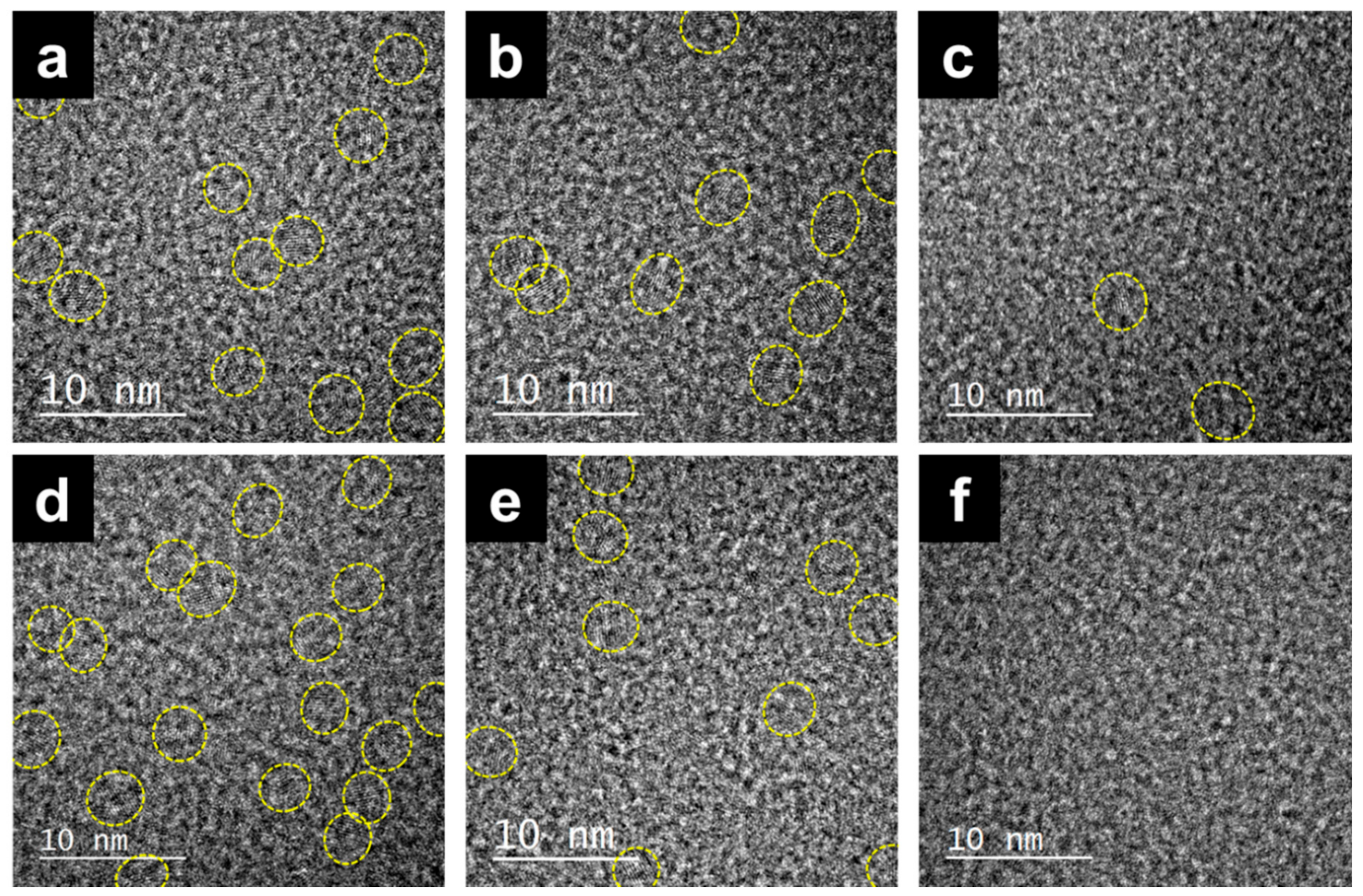
3.1. Capturing Charged NPs with Various Pressure during RF Sputtering with a Ti Target
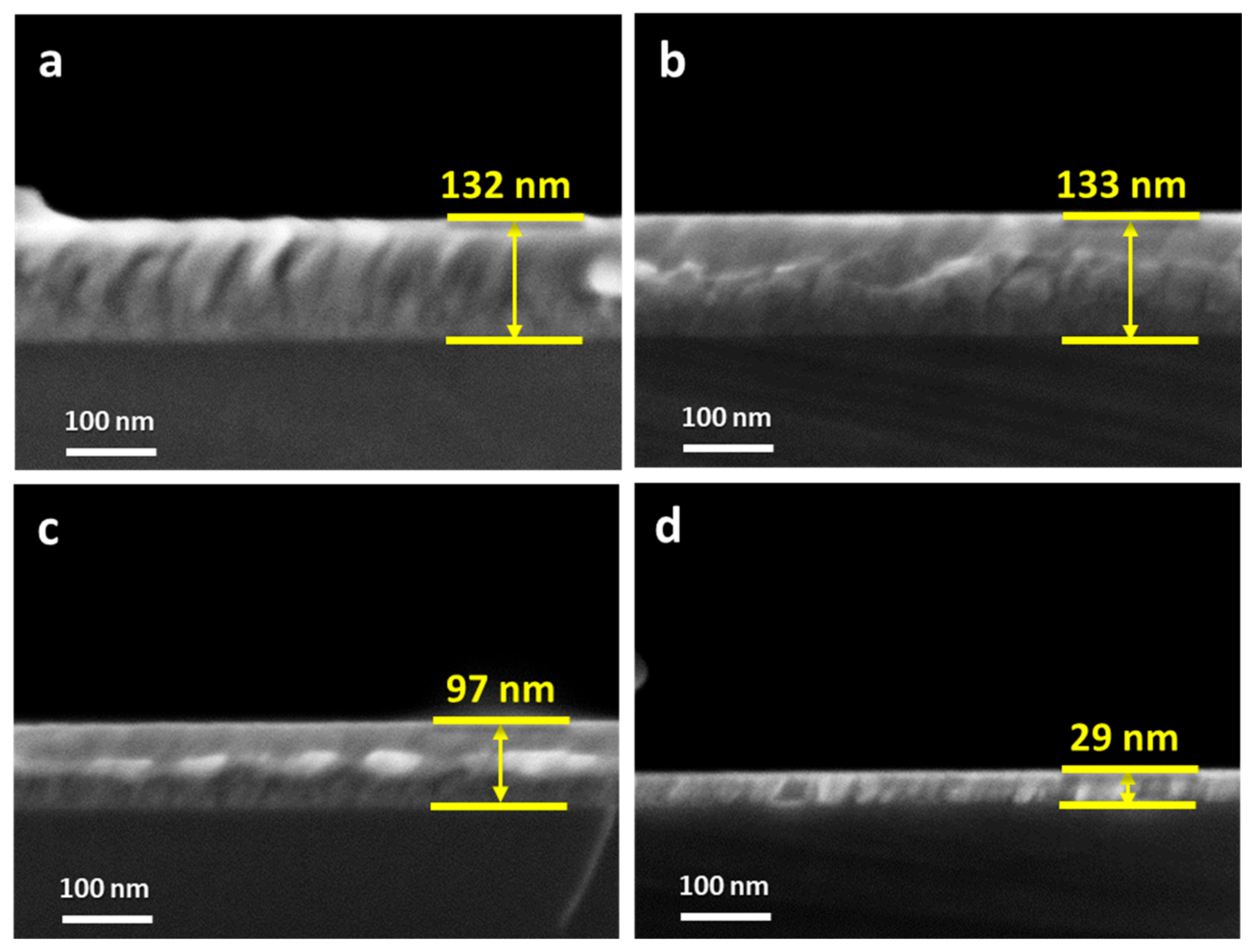
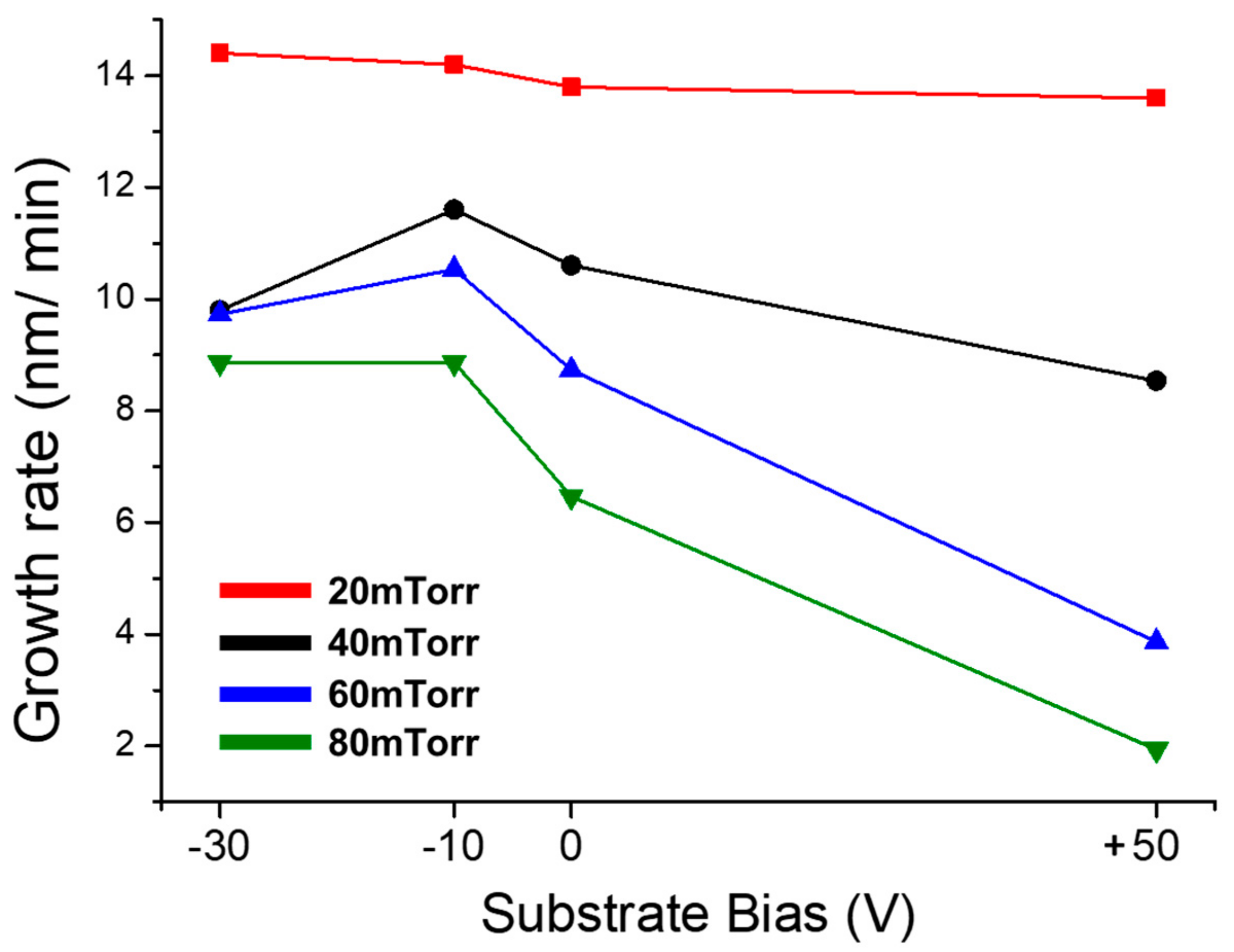
3.2. Deposition of Ti Thin Films under Various Pressures
4. Conclusions
Author Contributions
Funding
Institutional Review Board Statement
Informed Consent Statement
Data Availability Statement
Conflicts of Interest
References
- Boyer, R. An overview on the use of titanium in the aerospace industry. Mater. Sci. Eng. A 1996, 213, 103–114. [Google Scholar] [CrossRef]
- Elias, C.N.; Lima, J.H.C.; Valiev, R.; Meyers, M.A. Biomedical applications of titanium and its alloys. JOM 2008, 60, 46–49. [Google Scholar] [CrossRef]
- Kaur, M.; Singh, K. Review on titanium and titanium based alloys as biomaterials for orthopaedic applications. Mater. Sci. Eng. C 2019, 102, 844–862. [Google Scholar] [CrossRef]
- Ting, C.; Wittmer, M. The use of titanium-based contact barrier layers in silicon technology. Thin Solid Film. 1982, 96, 327–345. [Google Scholar] [CrossRef]
- Huang, L.; Liu, B.; Zhu, Q.; Chen, S.; Gao, M.; Qin, F.; Wang, D. Low resistance Ti Ohmic contacts to 4H–SiC by reducing barrier heights without high temperature annealing. Appl. Phys. Lett. 2012, 100, 263503. [Google Scholar] [CrossRef]
- Suzuki, M.; Kawakami, T.; Arai, T.; Kobayashi, S.; Koide, Y.; Uemura, T.; Shibata, N.; Murakami, M. Low-resistance Ta/Ti Ohmic contacts for p-type GaN. Appl. Phys. Lett. 1999, 74, 275–277. [Google Scholar] [CrossRef]
- Chawla, V.; Jayaganthan, R.; Chawla, A.K.; Chandra, R. Morphological study of magnetron sputtered Ti thin films on silicon substrate. Mater. Chem. Phys. 2008, 111, 414–418. [Google Scholar] [CrossRef]
- Chawla, V.; Jayaganthan, R.; Chawla, A.K.; Chandra, R. Microstructural characterizations of magnetron sputtered Ti films on glass substrate. J. Mater. Process. Technol. 2009, 209, 3444–3451. [Google Scholar] [CrossRef]
- Chen, A.Y.; Bu, Y.; Tang, Y.; Wang, Y.; Liu, F.; Xie, X.; Gu, J.; Pan, D. Deposition-rate dependence of orientation growth and crystallization of Ti thin films prepared by magnetron sputtering. Thin Solid Film. 2015, 574, 71–77. [Google Scholar] [CrossRef]
- Jeyachandran, Y.L.; Karunagaran, B.; Narayandass, S.; Mangalaraj, D. The effect of thickness on the properties of titanium films deposited by dc magnetron sputtering. Mater. Sci. Eng. A 2007, 458, 361–365. [Google Scholar] [CrossRef]
- Miyoshi, T.; Haga, Y.; Nittono, O. Microstructure and preferred orientation in pure titanium films deposited by two-facing-target-type DC sputtering. Thin Solid Film. 1996, 281, 128–131. [Google Scholar] [CrossRef]
- Muslim, N.; Soon, Y.W.; Lim, C.M.; Voo, Y.N. Influence of sputtering power on properties of titanium thin films deposited by RF magnetron sputtering. ARPN J. Eng. Appl. Sci. 2015, 10, 7148–7189. [Google Scholar]
- Audronis, M.; Bellido-Gonzalez, V. The effect of Ti sputter target oxidation level on reactive high power impulse magnetron sputtering process behaviour. Surf. Coat. Technol. 2011, 205, S322–S325. [Google Scholar] [CrossRef]
- Wu, B.; Yu, Y.; Wu, J.; Shchelkanov, I.; Ruzic, D.N.; Huang, N.; Leng, Y. Tailoring of titanium thin film properties in high power pulsed magnetron sputtering. Vacuum 2018, 150, 144–154. [Google Scholar] [CrossRef]
- Ghasemi, S.; Seyfi, P.; Farhadizadeh, A.; Ghomi, H. The experimental approach into the influence of external inductance on the discharge characteristic of HiPIMS. J. Theor. Appl. Phys. 2019, 13, 289–297. [Google Scholar] [CrossRef]
- Aizenberg, J.; Braun, P.V.; Wiltzius, P. Patterned colloidal deposition controlled by electrostatic and capillary forces. Phys. Rev. Lett. 2000, 84, 2997–3000. [Google Scholar] [CrossRef]
- Demortière, A.; Snezhko, A.; Sapozhnikov, M.V.; Becker, N.; Proslier, T.; Aranson, I.S. Self-assembled tunable networks of sticky colloidal particles. Nat. Commun. 2014, 5, 3117. [Google Scholar] [CrossRef]
- Ferrar, J.A.; Solomon, M.J. Kinetics of colloidal deposition, assembly, and crystallization in steady electric fields. Soft Matter 2015, 11, 3599–3611. [Google Scholar] [CrossRef]
- Sadri, B.; Pernitsky, D.J.; Sadrzadeh, M. Aggregation and deposition of colloidal particles: Effect of surface properties of collector beads. Colloids Surf. A Physicochem. Eng. Asp. 2017, 530, 46–52. [Google Scholar] [CrossRef]
- Wang, Z.; He, B.; Xu, G.; Wang, G.; Wang, J.; Feng, Y.; Su, D.; Chen, B.; Li, H.; Wu, Z.; et al. Transformable masks for colloidal nanosynthesis. Nat. Commun. 2018, 9, 563. [Google Scholar] [CrossRef]
- Kim, D.-S.; Hwang, N.-M. Synthesis of nanostructures using charged nanoparticles spontaneously generated in the gas phase during chemical vapor deposition. J. Phys. D Appl. Phys. 2018, 51, 463002. [Google Scholar] [CrossRef]
- Kim, C.-S.; Chung, Y.-B.; Youn, W.-K.; Hwang, N.-M. Generation of charged nanoparticles during synthesis of ZnO nanowires by carbothermal reduction. Aerosol Sci. Technol. 2009, 43, 120–125. [Google Scholar] [CrossRef]
- Hwang, N.M. Non-Classical Crystallization of Thin Films and Nanostructures in CVD and PVD Processes; Springer Netherlands: Dordrecht, The Netherlands, 2016; Volume 60, pp. 1–332. ISBN 978-94-017-7616-5. [Google Scholar]
- Jung, J.-S.; Lee, S.-H.; Kim, D.-S.; Kim, K.-S.; Park, S.-W.; Hwang, N.-M. Non-classical crystallization of silicon thin films during hot wire chemical vapor deposition. J. Cryst. Growth 2017, 458, 8–15. [Google Scholar] [CrossRef]
- Youn, W.-K.; Lee, S.-S.; Lee, J.-Y.; Kim, C.-S.; Hwang, N.-M.; Iijima, S. Comparison of the deposition behavior of charged silicon nanoparticles between floating and grounded substrates. J. Phys. Chem. C 2014, 118, 11946–11953. [Google Scholar] [CrossRef]
- Jeon, I.-D.; Barnes, M.; Kim, D.-Y.; Hwang, N.M. Origin of positive charging of nanometer-sized clusters generated during thermal evaporation of copper. J. Cryst. Growth 2003, 247, 623–630. [Google Scholar] [CrossRef]
- Park, S.-H.; Park, J.-W.; Yang, S.-M.; Kim, K.-H.; Hwang, N.-M. Effect of electric bias on the deposition behavior of ZnO nanostructures in the chemical vapor deposition process. J. Phys. Chem. C 2015, 119, 25047–25052. [Google Scholar] [CrossRef]
- Clare, B.W.; Talukder, G.; Jennings, P.J.; Cornish, J.C.L.; Hefter, G. Effect of charge on bond strength in hydrogenated amorphous silicon. J. Comput. Chem. 1994, 15, 644–652. [Google Scholar] [CrossRef]
- Kim, D.; Kim, D.Y.; Kwon, J.H.; Kim, K.-S.; Hwang, N.-M. Generation of charged SiC nanoparticles during HWCVD process. Electron. Mater. Lett. 2020, 16, 498–505. [Google Scholar] [CrossRef]
- Park, S.-W.; Jung, J.-S.; Kim, K.-S.; Kim, K.-H.; Hwang, N.-M. Effect of bias applied to the substrate on the low temperature growth of silicon epitaxial films during RF-PECVD. Cryst. Growth Des. 2018, 18, 5816–5823. [Google Scholar] [CrossRef]
- Jang, G.-S.; Kim, D.Y.; Hwang, N.-M. The effect of charged Ag nanoparticles on thin film growth during DC magnetron sputtering. Coatings 2020, 10, 736. [Google Scholar] [CrossRef]
- Kwon, J.H.; Kim, D.Y.; Hwang, N.-M. Generation of charged Ti nanoparticles and their deposition behavior with a substrate bias during RF magnetron sputtering. Coatings 2020, 10, 443. [Google Scholar] [CrossRef]
- Chapman, B.N. Glow Discharge Processes: Sputtering and Plasma Etching; Wiley: New York, NY, USA, 1980; pp. 1–406. ISBN 978-04-710-7828-9. [Google Scholar]
- Briot, O.; Moret, M.; Barbier, C.; Tiberj, A.; Peyre, H.; Sagna, A.; Contreras, S. Optimization of the properties of the molybdenum back contact deposited by radiofrequency sputtering for Cu(In1−xGax)Se2 solar cells. Sol. Energy Mater. Sol. Cells 2018, 174, 418–422. [Google Scholar] [CrossRef]
- Kampylafka, V.; Kostopoulos, A.; Modreanu, M.; Schmidt, M.; Gagaoudakis, E.; Tsagaraki, K.; Kontomitrou, V.; Konstantinidis, G.; Deligeorgis, G.; Kiriakidis, G.; et al. Long-term stability of transparent n/p ZnO homojunctions grown by rf-sputtering at room-temperature. J. Mater. 2019, 5, 428–435. [Google Scholar] [CrossRef]
- Acosta, M.; Méndez, R.A.; Riech, I.; Rodríguez-Pérez, M.; Rodríguez-Gattorno, G. Structural, optical and photoelectrochemical properties of tungsten oxide thin films grown by non-reactive RF-sputtering. Superlattices Microstruct. 2019, 127, 123–127. [Google Scholar] [CrossRef]
- Kwon, J.H.; Kim, D.Y.; Kim, K.-S.; Hwang, N.-M. Preparation of highly (002) oriented Ti films on a floating Si (100) substrate by RF magnetron sputtering. Electron. Mater. Lett. 2019, 16, 14–21. [Google Scholar] [CrossRef]


Publisher’s Note: MDPI stays neutral with regard to jurisdictional claims in published maps and institutional affiliations. |
© 2021 by the authors. Licensee MDPI, Basel, Switzerland. This article is an open access article distributed under the terms and conditions of the Creative Commons Attribution (CC BY) license (http://creativecommons.org/licenses/by/4.0/).
Share and Cite
Kim, D.-Y.; Kwon, J.-H.; Jang, G.-S.; Hwang, N.-M. Effect of Pressure on the Film Deposition during RF Magnetron Sputtering Considering Charged Nanoparticles. Coatings 2021, 11, 132. https://doi.org/10.3390/coatings11020132
Kim D-Y, Kwon J-H, Jang G-S, Hwang N-M. Effect of Pressure on the Film Deposition during RF Magnetron Sputtering Considering Charged Nanoparticles. Coatings. 2021; 11(2):132. https://doi.org/10.3390/coatings11020132
Chicago/Turabian StyleKim, Du-Yun, Ji-Hye Kwon, Gil-Su Jang, and Nong-Moon Hwang. 2021. "Effect of Pressure on the Film Deposition during RF Magnetron Sputtering Considering Charged Nanoparticles" Coatings 11, no. 2: 132. https://doi.org/10.3390/coatings11020132
APA StyleKim, D.-Y., Kwon, J.-H., Jang, G.-S., & Hwang, N.-M. (2021). Effect of Pressure on the Film Deposition during RF Magnetron Sputtering Considering Charged Nanoparticles. Coatings, 11(2), 132. https://doi.org/10.3390/coatings11020132