Article

Microring Zone Structure for Near-Field Probes

Department of Physics, University of Zilina, 01026 Zilina, Slovakia
*
Author to whom correspondence should be addressed.
Coatings 2021, 11(11), 1363; https://doi.org/10.3390/coatings11111363
Submission received: 30 September 2021 / Revised: 27 October 2021 / Accepted: 30 October 2021 / Published: 5 November 2021
(This article belongs to the Special Issue Metal/Dielectric Structures for Surface Plasmon Resonance)

Abstract

:
Recent advances in Surface Plasmon Resonance (SPR) technologies have shown the possibility of transmission enhancement of localized modes propagating through sub-diffraction wide slits and apertures, resulting in the strong near-field focusing of metallic planar nanostructures. This work presents a new approach to the fabrication of high-resolution near-field optical probes using 3D lithography in combination with numerical finite difference time domain (FDTD) simulations. A narrow 500 nm depth of field focus area was observed both by numerical analysis and near field scanning optical microscopy (NSOM) measurements. Further research and optimization are planned in order to achieve subwavelength focal regions and increased signal intensities.

1. Introduction

Surface plasmon resonance (SPR) brings a novel approach for lab-on-fiber nanoprobes with highly resolved sensing. SPR is an optical phenomenon describing the propagation of electromagnetic (EM) waves along with the metal-dielectric interface. These confined modes called Surface Plasmons (SPs) are induced by incident EM radiation resulting in the coherent collective oscillation of conduction electrons at the metal’s surface [1]. The evanescent character of these waves indicates the finite propagation lengths perpendicular to the interface as well as along the interface itself, however in the vicinity of the metal layer, the EM fields exhibit an exceptional enhancement originating from the resonant behavior of the electrons and wavelength of incident radiation. Properties of SPs depend predominantly on frequency-dependent relative permittivity of the metal and dielectric materials. However, the use of nanopatterned surfaces with exact geometry allows the manipulation of the resonant wavelength of the SPs as well as near-field properties in the proximity of the surface [2].
The evanescent decay of the modes enabled the construction of two-dimensional (2D) optical elements such as interferometers, waveguides and mirrors [3,4,5]. Liu et al. demonstrated focusing of the SPs using a series of circular and elliptical nanostructures fabricated in thin metal films [6]. They were able to achieve sub-diffraction focal spots using interfering plasmons propagating through metal slits. Ogut et al. fabricated a plasmonic parabolic transducer with a multi-layer configuration achieving focal spots beyond the diffraction limit by varying the refractive index of the dielectric material [7]. Mote et al. numerically investigated the near-field focusing properties of zone plates coated with different metal films of 300 nm, indicating no presence of the SPs. Later they proposed a 2D flat design achieving sub-wavelength resolution according to the simulations [8,9]. Another numerical study conducted by Wang et al. aimed to address the issue of the transmission enhancement through a sub-wavelength aperture surrounded by annular grooves of various depths in the 200 nm thin silver film achieving full width at half maximum (FWHM) of 0.85λ and 1.1λ in the lateral and transverse direction, respectively [10]. Progress in nano-optics gave rise to numerous applications such as near-field scanning optical microscopy (NSOM), sub-diffraction lithography, surface enhanced Raman scattering (SERS), and nano-manipulation of the organic specimen using SPR optical tweezers [11,12]. Recently, focusing on decaying plasmons in the near field has obtained interest as a result of the unique enhanced transmission. Therefore, by focusing on the evanescent components it is possible to overcome the conventional barrier caused by the diffraction limit resulting in nanometer size focal spots [13]. Fu et al. [14] presented a plasmonic micro-zone-plate introducing the metal dielectric interface in conventional Fresnel zone plate structure. They achieved superfocusing with a resolving power beyond the diffraction limit.
Generally, all the achieved results employed planar technologies resulting in 2D optical elements. The idea behind this paper was to upgrade the SPR effects on more complex three-dimensional (3D) plasmonic structures based on a Fresnel zone plate design resulting in a microring-zone (MRZ) structure with the polymer-metal interface. As a key technology we use 3D laser lithography based on non-linear two-photon absorption (TPA) and deposition of a thin gold layer on top of the prepared polymer structure. The MRZ structure should reach strong enhancement in the near-field region with unique focusing properties with a submicrometer depth of field and resolution. These properties make the MRZ structure perspective probe for near-field probes and application. Here we proposed and realized a new concept of 3D microring-zone structure supported by complete theoretical simulations and near-field measurements using a near-field scanning optical microscope (NSOM) to determine the plasmon focusing properties of the sample.

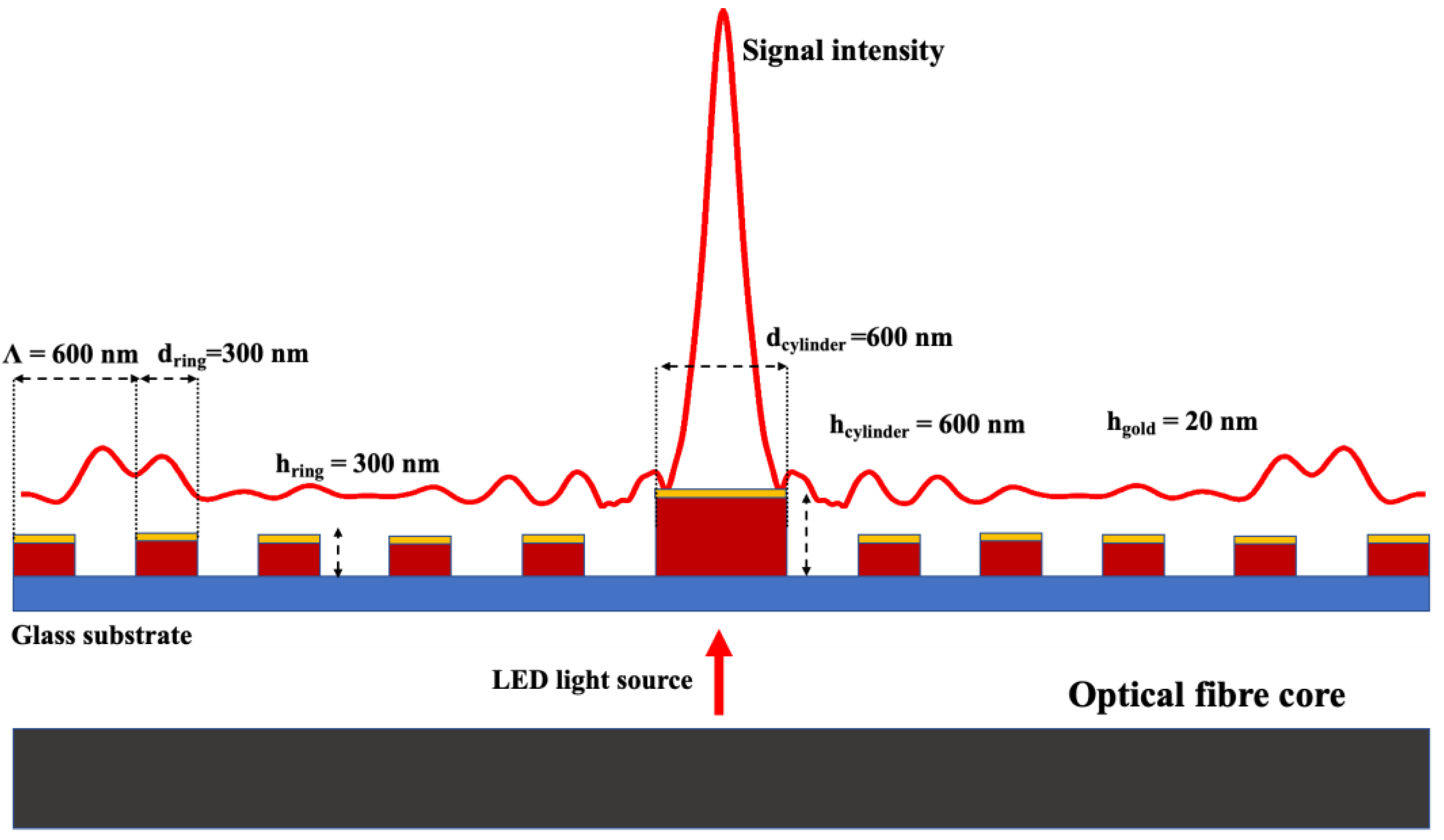
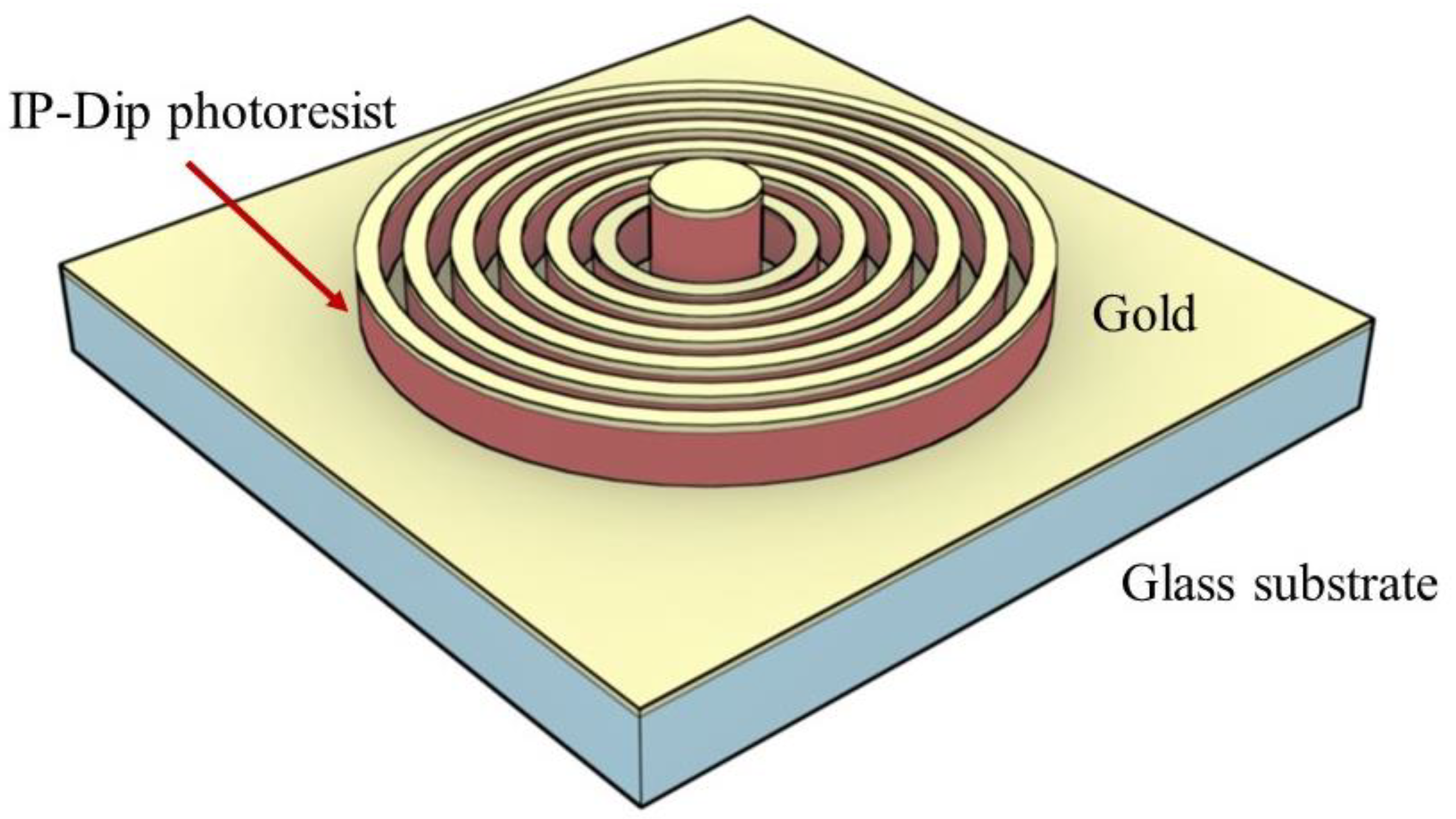
2. Design and Simulation of Microring-Zone Structure

The explicit numerical analysis of plasmonic micro-zone plates documented apparent relations between the propagation of an EM wave through a planar structure with conventional Fresnel zones plates and plasmonic micro-zone plates. Adding the metallic layer suppressed the multiple focal points in the far-field, as is typical for conventional Fresnel zone plates with dominant extremes and in very short distance from the surface, and also overcame the diffraction limits.
Our concept implies equidistant zone distribution with different heights of the central ring. As a material basis we used a glass substrate with polymer structure based on IP-Dip photoresist with 20 nm gold layer deposited on the surface (Figure 1). The MRZ structure consists of six individual rings with a width of 250 nm and a height of 300 nm separated by a 250 nm spacer and central part with the radius of 600 nm and doubled height. The total MRZ structure diameter is 7.2 µm.
Focusing itself occurs when the incident plane wave hits the MRZ structure, inducing SPs propagating along the surface and evanescently decaying in the normal direction. At the end of the MRZ structure, the evanescent wave transforms into propagation mode and radiates behind the MRZ surface. Arranging the rings and spacers in a particular geometry, a phase modulation with the following interference leads to the formation of a focal spot behind the MRZ structure. This was demonstrated in many similar zone plate structures [15]. Due to technological simplification, we used an equidistant arrangement of the microring zones with the same spacer distance. Such a design will not have a fully optimized phase modulation and weak side interference as expected. The thickness of microrings of 250 nm and the same spacer distance is very close to the technological limits of 3D laser lithography, which limits the design of asymmetric microring distribution. Cross-section of the MRZ structure with simulated optical field distribution is shown in Figure 2.
We used a Finite-Difference Time-Domain (FDTD) tool from Ansys—Lumerical to simulate an optical field distribution behind the MRZ structure after illumination by different light sources. A uniform mesh step size of 30 nm was set up while the volume of simulation in the region was 10 × 10 × 6 µm3. A perfectly matched layer boundary condition was applied at the edges of the simulation region along with a 5 nm uniform mesh step size. For the gold layer we used the Johnson and Christy model of the optical constants of the noble metals [11]. The structure was illuminated from the glass side using the light-emitting diodes (LEDs) plane wave source with different wavelengths of 420, 490, 625 and 780 nm, respectively. According to the equation describing the SPP propagating along with the metal-dielectric interface, the SP’s can only be excited when one of the permittivities is negative and its absolute value exceeds the other material permittivity. The plasmon propagation constant along the interface is then given by the known equation:
β = k 0 ε d ε m ε d + ε m ,
where k0 is the wavevector of the incident wave and εd and εm are the permittivities of the dielectric and metal, respectively. Assuming that the solution is bound to the interface, propagation constants normal to the metal-dielectric interface are both real and imaginary, leading to the exponential decay of the field into the dielectric [12,13]. This is only satisfied for the wavelength of 420 nm and lower, where the real part of permittivity of gold εAu = −2.462 with an absolute value higher than the permittivity of the used photoresist. Table 1 shows the corresponding values of real dielectric constants for 20 nm thin gold layer and IP-Dip photoresist for considered wavelengths. Thus, the increasing wavelength mostly propagates dominantly along the surface and doesn’t contribute to focusing, as was calculated by FDTD (Figure 3). The exit plane of the MRZ structure is located at z = 1.8 μm. At the IP-Dip/gold interface, a part of the incident radiation is converted from propagating beam into the evanescent waves, which due to the thin gold layer are transmitted to the exit plane of the structure, where the conversion back to the propagating mode associated with its interference with diffracted modes from the microring zones occurs [14]. Simulation shows that further increasing the wavelength enhances the outer diffraction emission instead of focusing on what agrees well with the described theory of SP’s propagation. This is due to the dispersion behavior of the metal’s dielectric function, which at higher wavelengths does not satisfy the resonance condition.
Another effect of the increasing wavelength is the existence of multiple focal points behind the MRZ structure (as shown in Figure 3d,f,h) resulting from odd-order diffraction patterns which have been previously observed by multiple groups [16,17]. Formation of the dominant focus shown in Figure 3a,b with Full-Width at Half-Maximum (FWHM) around 630 nm resulted from constructive interference of the SPs at the exit plane of the nanostructure. By optimization of the refractive index of the dielectric or metal, one can exactly manipulate the phase conditions of propagating waves to enhance or suppress their interference.

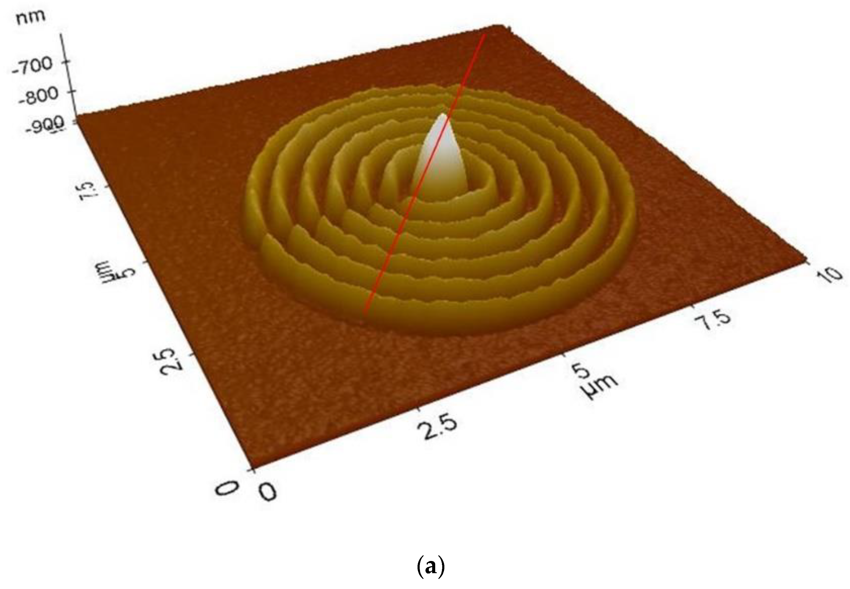
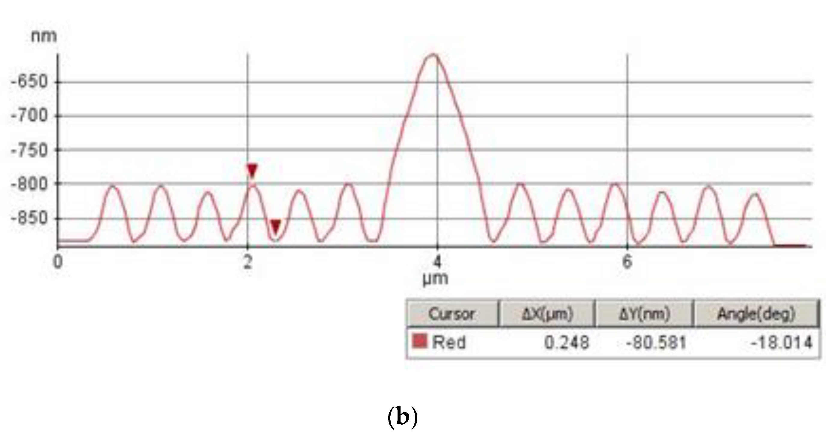
3. Fabrication and Structure Analysis

The structure was fabricated using Direct Laser Writing (DLW) system from Nanoscribe GmbH (Karlsruhe, Germany), using the TPA process causing polymerization of small focal volume located in negative IP-Dip photoresist. Two-photon polymerization (TPP) is a non-linear process based on the simultaneous absorption of two photons in a photosensitive material, activating photo-initiators in the resist resulting in the formation of radicals suitable for the local polymerization. This process requires high intensities, commonly provided by the femtosecond laser beam tightly focused by an immersive microscope objective with a high numerical aperture. Such high intensities are present only in the small confined area within the focus of the objective, thus providing extraordinary spatial resolution. The wavelength of the femtosecond laser built in the device is 780 nm with a pulse duration of 100 fs. This system serves as a lithography method intended to fabricate 3D polymer submicrometer sized structures. We used Dip-in Laser Lithography (DiLL) configuration where a microscope objective with 63× magnification and numerical aperture of 1.4 is directly dipped into the photoresist, minimizing spherical aberrations. In that configuration, the DLW system can sufficiently achieve lateral feature size better than 200 nm and 500 nm in the axial direction. Overall, the height of the structure is limited by the optical power within the volume of the TPA region as well as the scanning speed. In the first step we fabricated a radially symmetrical MRZ structure with 250 nm wide slits and 250 nm wide rings, with a 600 nm radius cylinder located in the middle of the structure according to the design. The sample was developed afterward in propylene glycol methyl ether acetate (PGMEA) developer for seven min followed by a five-min bath in isopropyl alcohol. As the final step, a 20 nm layer of gold was deposited using thermal evaporation in a vacuum chamber with a pressure of 6 × 10⁻⁴ mbar and deposition rate of 2.1 Å/s. The morphology of the sample was measured by atomic force microscopy (AFM, XE100, Park Systems Europe GmbH, Mannheim, Germany), and shown in Figure 4.
The overall structure has a diameter of 7.25 µm and a central ring slightly under 1.2 µm. Also, other rings are separated nearly by 248 nm, which agrees well with the design. Because the microrings of the MRZ reach the limits of the lateral resolution of Nanoscribe lithography, we chose to directly write the structure as a function of radius and angle instead of scanning the volume horizontally. As a consequence of this, during the step-TPA fabrication of the innermost cylinder, the power absorbed in the TPA volume limited by Nanoscribe’s voxel size was considerably higher than previously designed, resulting in the polymerization of the upraised volume of IP-Dip resist and creating its conical shape. However, the simulations accounted for this. For high-resolution characterization of optical fields in proximity of the MRZ structure we used near field scanning optical microscopy (NSOM). The NSOM arrangement and working principle are shown in Figure 5.
By scanning an optical fiber probe in the near-field region of the MRZ structure we obtained a near-field image of the optical field in desired scanning planes with respect to the structure surface. During the scanning process the MRZ structure was illuminated by different LED sources coupled to the SMF.

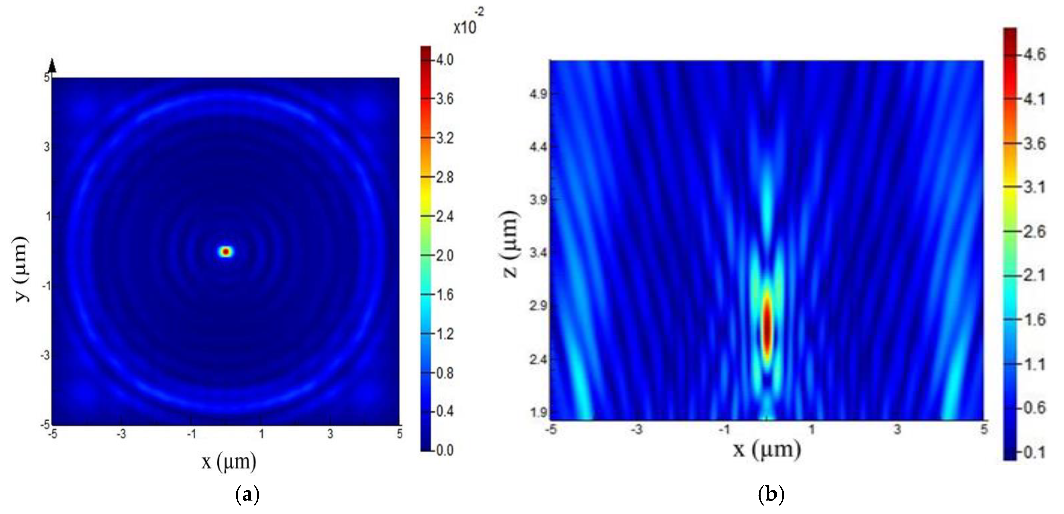
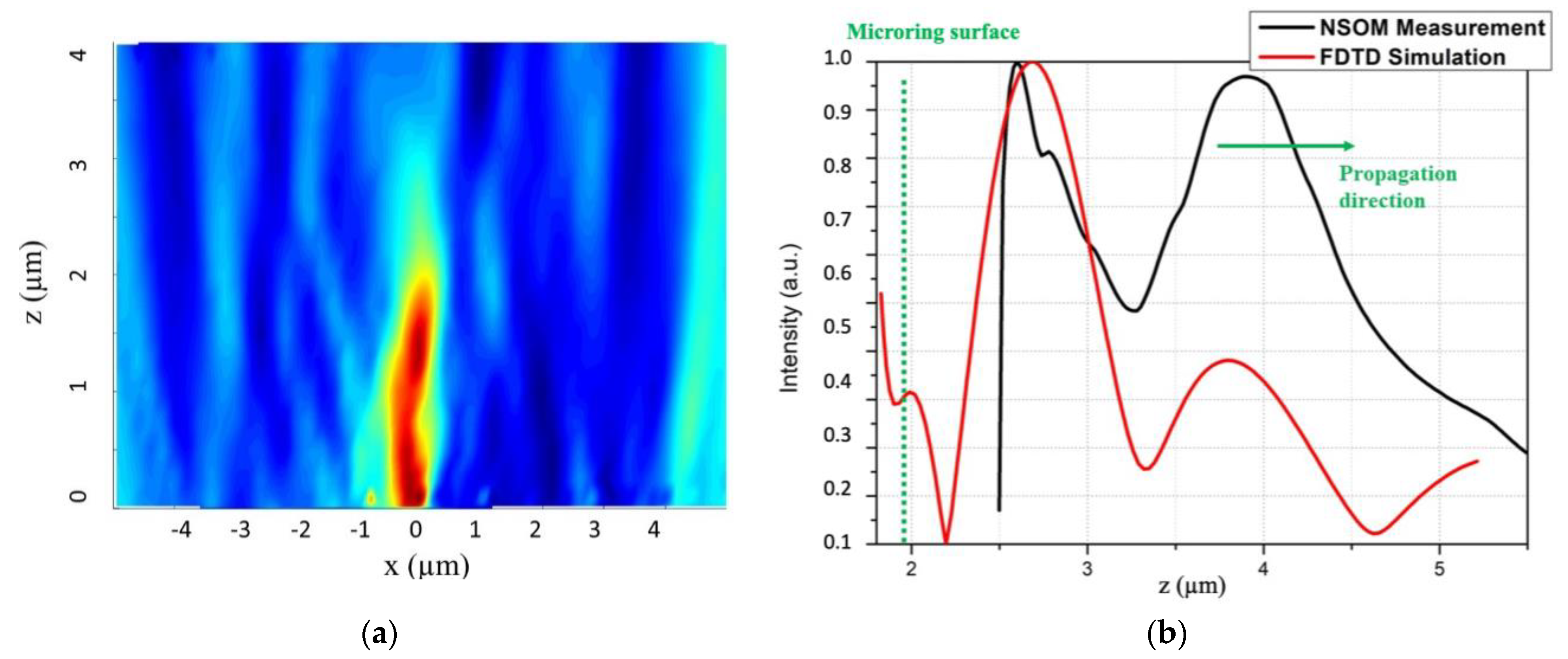
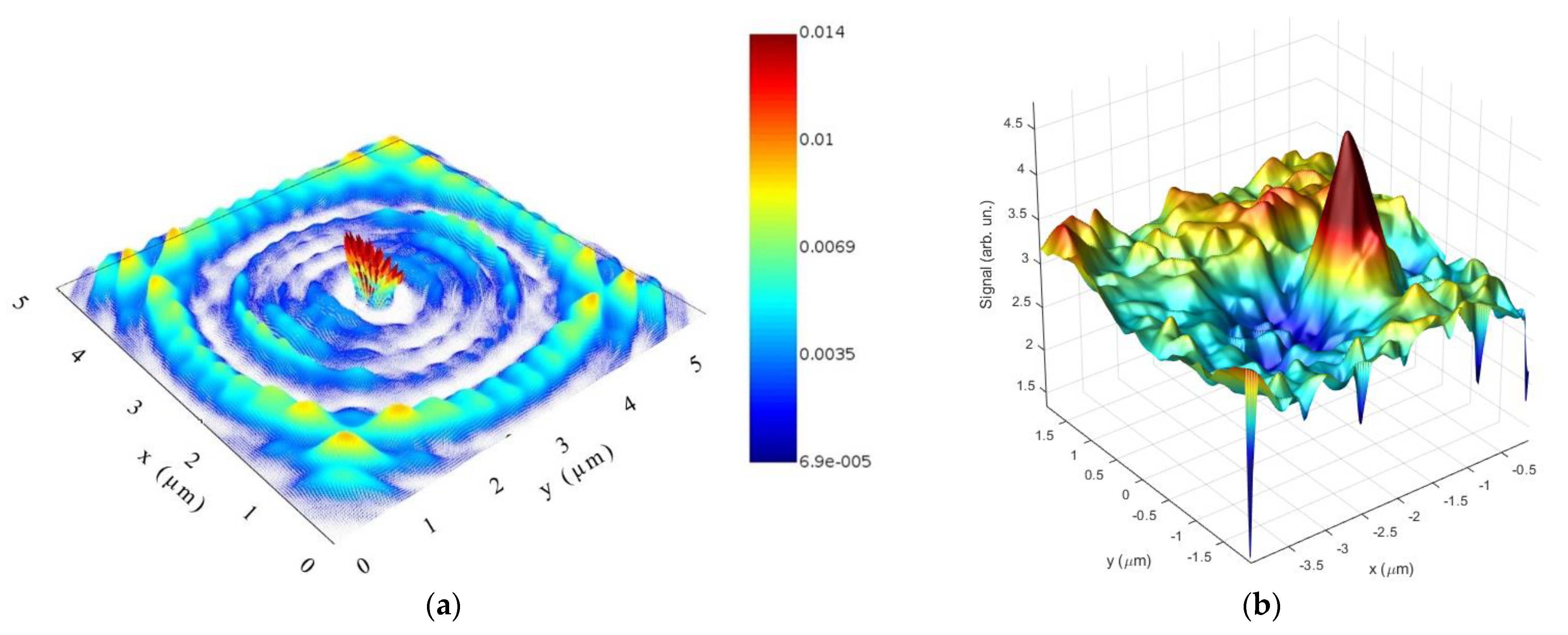
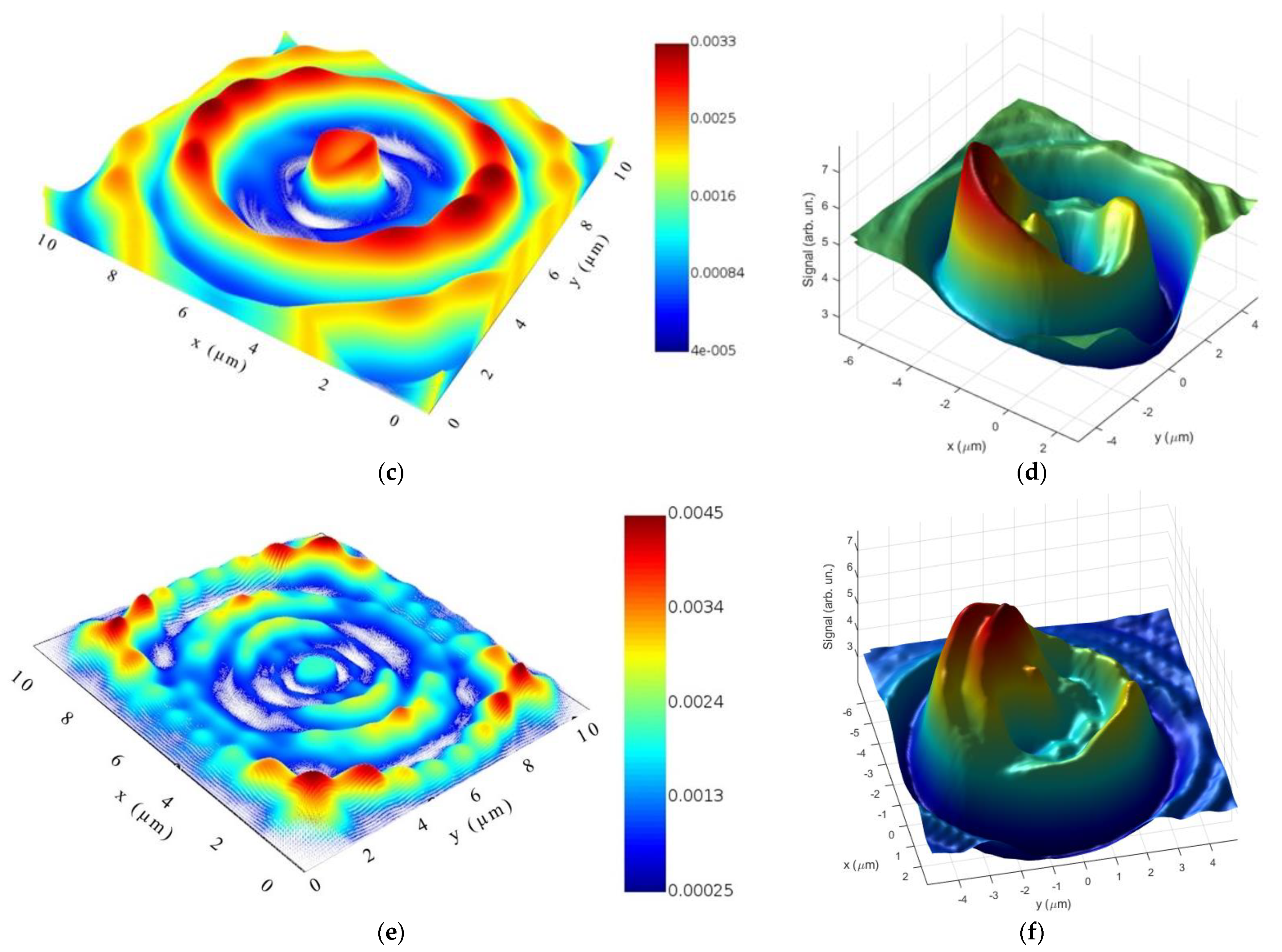
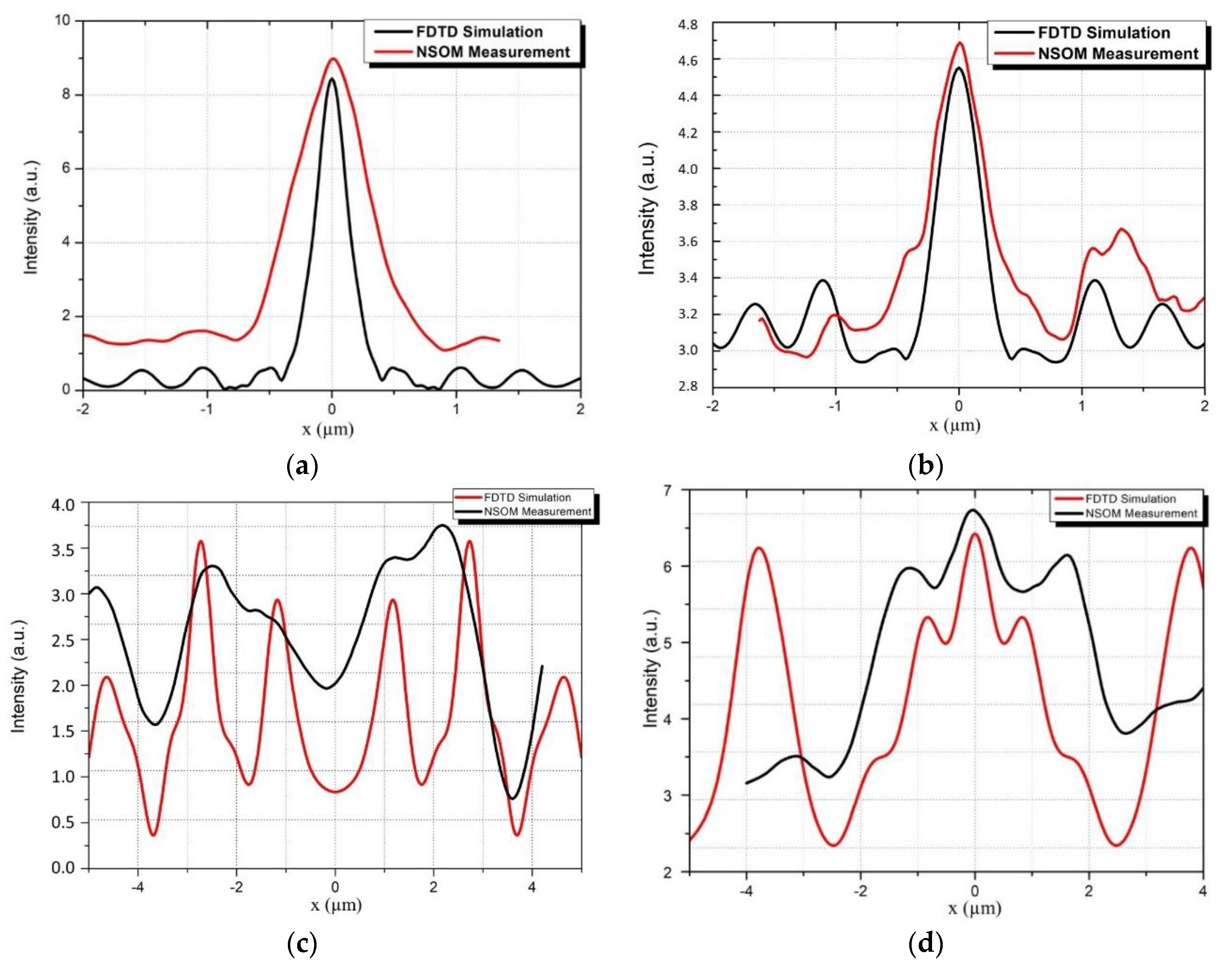
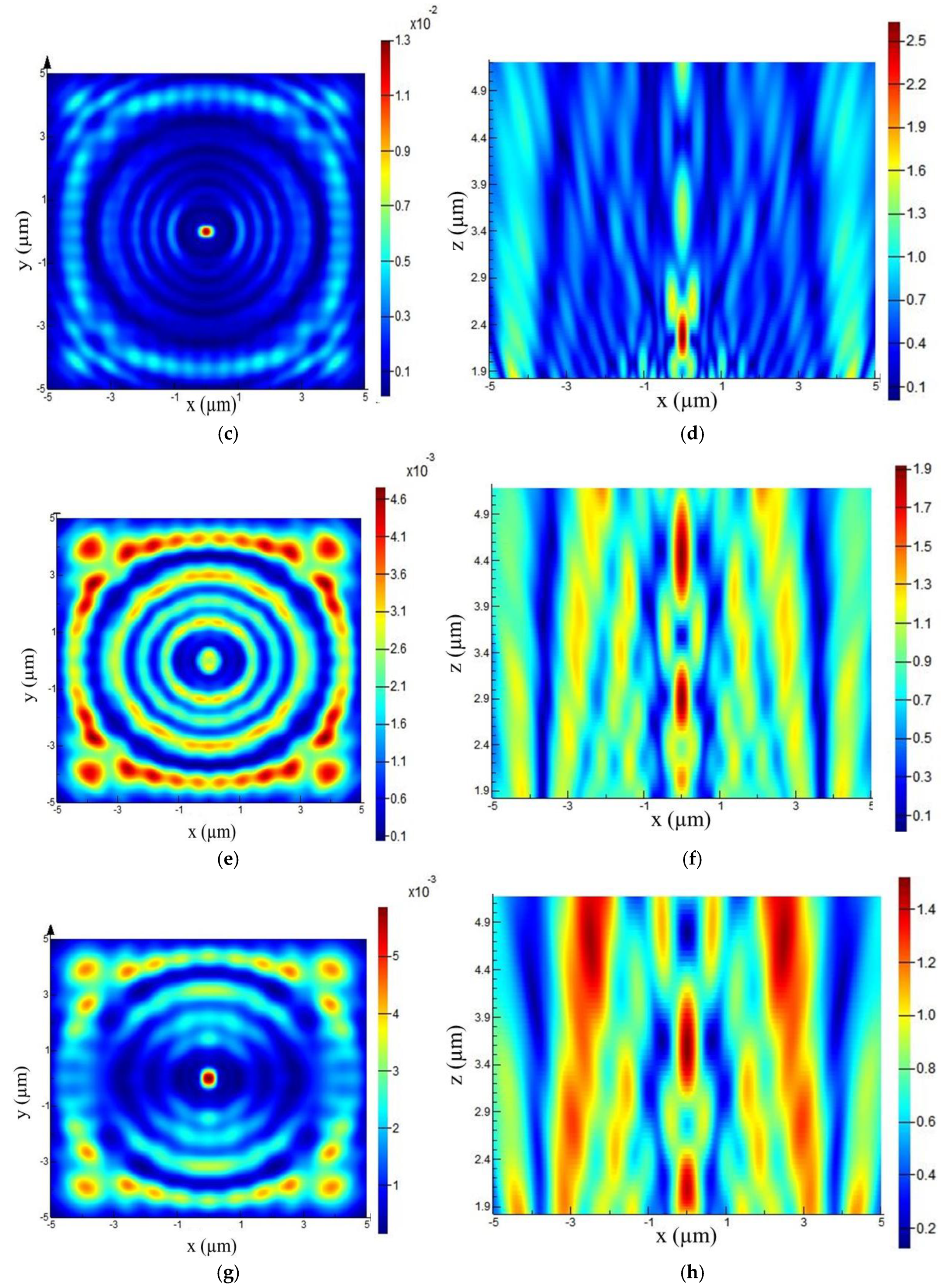
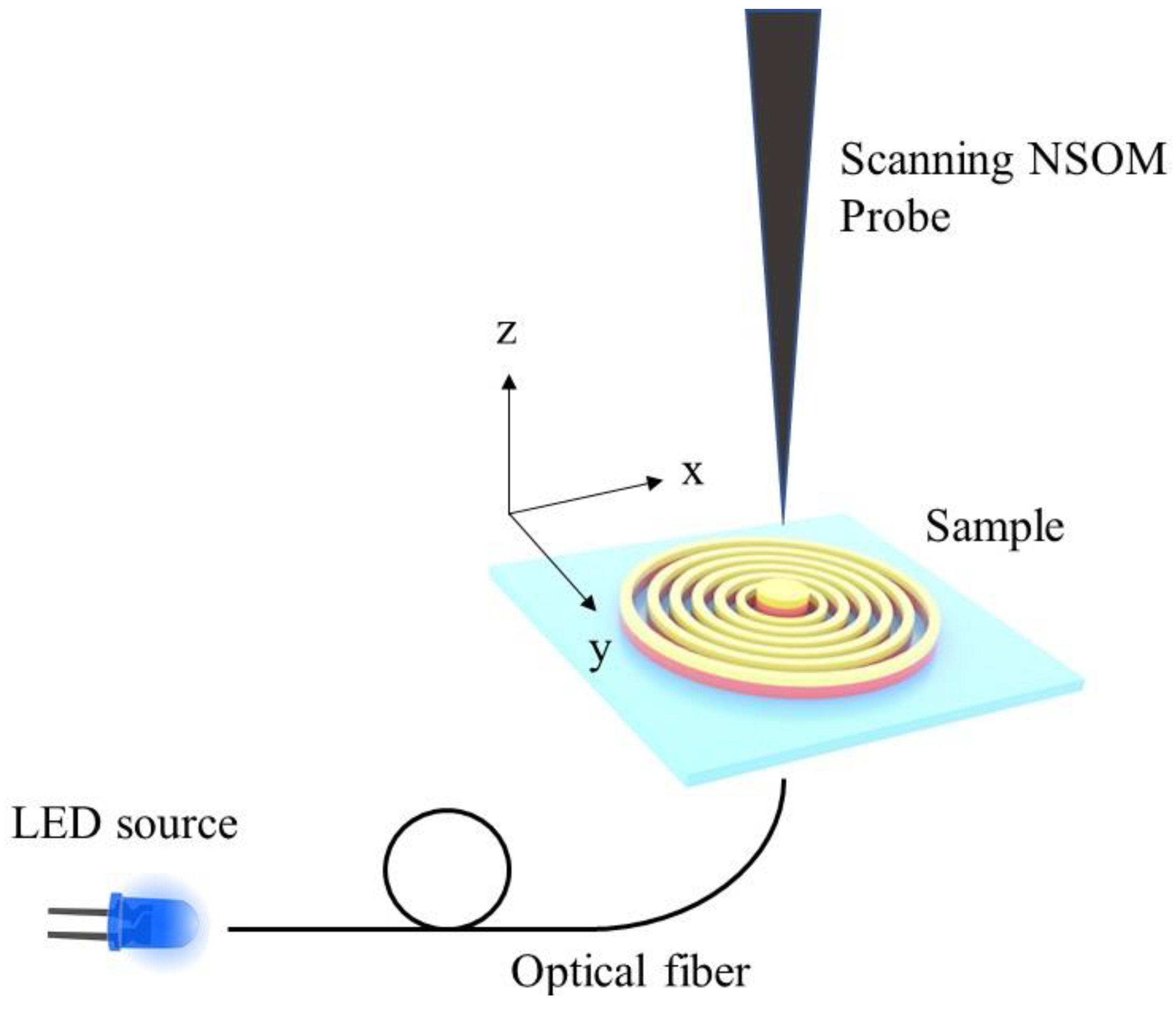
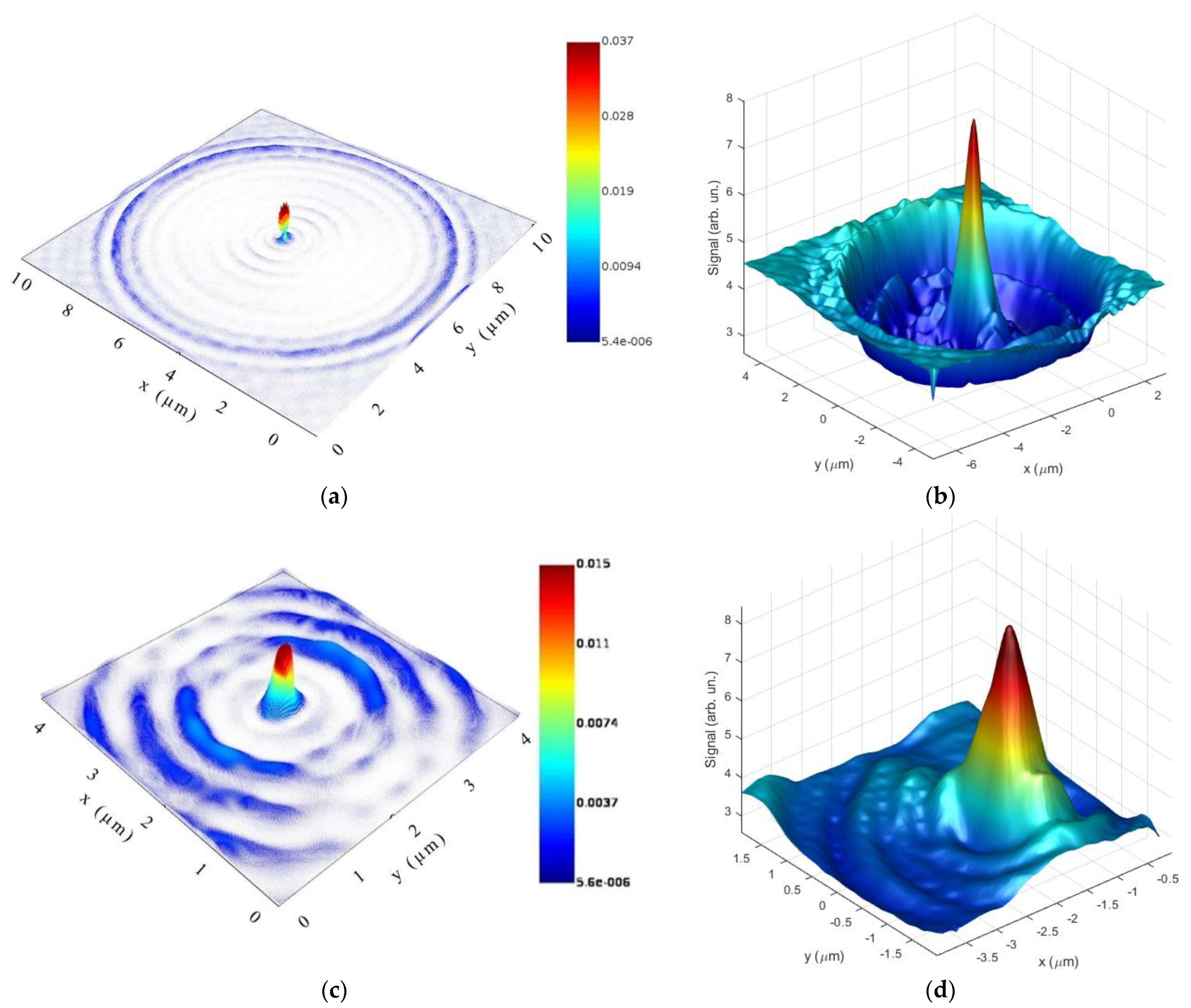
4. Results—Near-Field Analysis

The crucial analysis for characterization of optical properties of MRZ structures is the near-field distribution measured by NSOM in transmission mode, as was described in Figure 5. The MRZ structure was excited by different LED sources coupled to the standard single-mode optical fiber with 10 µm core diameter in order to sufficiently illuminate the whole MRZ structure. It is also worth mentioning that the fiber operates in single mode regime at the wavelength of 1550 nm and the used LED wavelengths will create a multimodal propagation. Simulated and measured near-field maps for illumination by a 420 nm LED source are compared in Figure 6 and confirm a light intensity enhancement behind the central ring of the MRZ structure. Simulated near-field distribution agrees well with the measured near-field signal. The strong, sharp signal was observed both in simulation and NSOM measurement with full width at half maximum (FWHM) of 630 nm and an enhancement factor of almost 800% with respect to the planar surface of the IP-Dip polymer with deposited 20 nm thin gold layer.
In the next investigation, we tried to resolve the focusing properties and depth of field by characterization of the optical field in the propagation direction (z axis direction). Figure 7 shows the comparison of FDTD simulated electric field intensity with NSOM measurement of the MRZ structure back-illuminated by 420 nm by a non-polarized LED source. Measured optical field distribution documents light propagation in a very narrow region behind the central part of the MRZ structure with two dominant maxima (Figure 7a). Their position was compared with the simulated optical field profile (Figure 7b).
We also characterized a spectrally resolved response of the near-field emission. The MRZ structure was illuminated by LED sources of different wavelengths (490, 625 and 780 nm) in the same experimental setup. The central enhancement gradually vanishes with the increasing wavelength of the incident radiation due to the attenuation given by the diffraction phenomena (Figure 8). The diffraction and interference of higher wavelengths cause enhanced emission just inside the outside regions. It is also worth mentioning that the measured near-field response of the MRZ structure illuminated by the 625 nm and 780 nm LED source shown in Figure 8d,f indicates a slightly asymmetric emission pattern not previously predicted by simulations.
The pattern is caused by the small surface irregularities in the outer part of the MRZ structure. However, the measurement and simulation at longer wavelengths clearly favor the MRZ structure for the shorter spectral regions, as was considered in the design. This was previously numerically predicted and confirmed by Liu et al. [18]. Simulation and experimentally measured near-field profiles document a very similar field distribution in the Figure 9. The small differences are given only by the resolution limits of technology and NSOM analysis. The reason behind this is the already mentioned lateral resolution limit of the lithography system, which produces rounded rather than sharp edges as was considered in the designed structure. On the other hand, NSOM analysis also reaches resolution limits by detecting micro-ring spacers. However, the NSOM analysis revealed the highly resolved near-field behind the MRZ structure, which fits well with the FDTD simulations for all mentioned wavelengths.
Fresnel zone plates are known to generate multiple interference peaks in the far-field along the propagation axis, which our design suppresses quite substantially. We chose the equidistant periodic ring design in order to achieve uniform ∆k gain of the diffracted modes so multiple wavelengths could induce the SPPs at the edges of the rings. Generally, the proposed MRZ structures with equidistant zones don’t bring effective interference while creating weak parasitic side peaks in the near field region, which standard Fresnel zone plates eliminate. Also, using equidistant zones is more convenient from the point of manufacturing using the single step laser lithography process. Regardless, more optimization is needed in the forthcoming design and manufacturing.

5. Conclusions

We demonstrated the 3D concept of plasmonic MRZ structure on the polymer-metal basis with strong near-field transmission enhanced by surface plasmon resonance. The MRZ structure consists of multiple equidistant rings designed in a 3D arrangement with central ring of doubled height. Simulation in FDTD and near-field measurements revealed very narrow focus with a 500 nm depth of field produced by the combination of phase modulation on MRZ structure and SP’s effect at the IP-Dip/gold interface. Observed formation of the high-intensity focal spot with FWHM of 630 nm and an enhancement factor of ~8 was numerically calculated and experimentally confirmed by NSOM measurements. We also inspected the effect of wavelength change on the transmission properties as this MRZ structure was designed for wavelengths of 420 nm. Longer wavelengths confirmed the better SP’s propagation along with the polymer/metal interface with a stronger effect of interference. This effect suppressed the central focus and enhanced the outer extremes produced by multiple zones of the MRZ structure. It was documented from FDTD analysis but also from near-field maps of the MRZ structure by higher excitation wavelengths. The prepared MRZ structure documents good focusing properties and will be applied on the optical fiber to produce special near-field probes. In contrast with [19,20,21] this proposed design requires fewer fabrication steps and offers promising applications such as integration on the tip of optical fiber. At the same time, these results open new horizons where modern 3D laser technologies on a polymer basis could be applied on the submicrometer scale and used for near-field probes. Further research also should be oriented to the next optimization of focusing on the introduction of more complicated 3D designs to reach subwavelength focal regions as well as higher signal enhancement.

Author Contributions

Conceptualization, P.M.; experimental, P.G. and D.J.; structure analysis, J.D. and D.P.; writing—review and editing, D.P. and P.M.; methodology, P.G. and D.J.; validation, J.D. and D.P. All authors have read and agreed to the published version of the manuscript.

Funding

This work was supported by the Slovak National Grant Agency under project No. VEGA 1/0540/18 and the Slovak Research and Development Agency under the project No. APVV-20-0264. This paper was supported under the project of Operational Programme Integrated Infrastructure: Independent research and development of technological kits based on wearable electronics products, as tools for raising hygienic standards in a society exposed to the virus causing the COVID-19 disease, ITMS2014+ code 313011ASK8. The project is co-funding by European Regional Development Fund.

Institutional Review Board Statement

Not applicable.

Informed Consent Statement

Not applicable.

Data Availability Statement

Data sharing is not applicable to this article.

Acknowledgments

I would like to thank my colleagues and their guidance during all the individual steps of the fabrication and characterization processes. My deepest acknowledgments belong to my fiancée, whose constant support inspires and motivates me through the pandemic.

Conflicts of Interest

The authors declare no conflict of interest.

References

  1. Novotny, L.H.B. Principles of Nano-Optics, 2nd ed.; Cambridge University Press: Cambridge, UK, 2012. [Google Scholar]
  2. Nickelson, L. Electromagnetic Theory and Plasmonics for Engineers; Springer: Vilnius, Lithuania, 2019. [Google Scholar] [CrossRef]
  3. Krenn, J.R.; Weeber, J.-C. Surface plasmon polaritons in metal stripes and wires. Philos. Trans. R. Soc. A Math. Phys. Eng. Sci. 2004, 362, 739–756. [Google Scholar] [CrossRef] [PubMed]
  4. Raether, H. Surface Plasmons on Smooth and Rough Surfaces and on Gratings; Springer: Berlin/Heidelberg, Germany, 1988. [Google Scholar] [CrossRef]
  5. Ditlbacher, H.; Krenn, J.; Schider, G.; Leitner, A.; Aussenegg, F.R. Two-dimensional optics with surface plasmon polaritons. Appl. Phys. Lett. 2002, 81, 1762–1764. [Google Scholar] [CrossRef]
  6. Liu, Z.; Steele, J.M.; Srituravanich, W.; Pikus, Y.; Sun, A.C.; Zhang, X. Focusing Surface Plasmons with a Plasmonic Lens. Nano Lett. 2005, 5, 1726–1729. [Google Scholar] [CrossRef] [PubMed]
  7. Ogut, E.; Yanik, C.; Kaya, I.I.; Ow-Yang, C.; Sendur, K. Focusing short-wavelength surface plasmons by a plasmonic mirror. Opt. Lett. 2018, 43, 2208–2211. [Google Scholar] [CrossRef] [PubMed]
  8. Mote, R.G.; Yu, S.F.; Ng, B.K.; Zhou, W.; Lau, S.P. Near-field focusing properties of zone plates in visible regime—New insights. Opt. Express 2008, 16, 9554–9564. [Google Scholar] [CrossRef] [PubMed]
  9. Mote, R.G.; Minin, O.V.; Minin, I.V. Focusing behavior of 2-dimensional plasmonic conical zone plate. Opt. Quantum Electron. 2017, 49, 271. [Google Scholar] [CrossRef]
  10. Wang, J.; Zhou, W. Subwavelength beaming using depth-tuned annular nanostructures. J. Mod. Opt. 2009, 56, 919–926. [Google Scholar] [CrossRef]
  11. Johnson, P.B.; Christy, R.W. Optical Constanst of the Noble Metals. Phys. Rev. B 1972, 6, 4370. [Google Scholar] [CrossRef]
  12. Dryakhlushin, V.F.; Klimov, A.Y. Near-field optical lithography method for fabrication of the nano dimensional objects. Appl. Surf. Sci. 2005, 248, 200–203. [Google Scholar] [CrossRef]
  13. Huang, J.-S.; Yang, Y.-T. Origin and Future of Plasmonic Optical Tweezers. Nanomaterials 2015, 5, 1048–1065. [Google Scholar] [CrossRef] [PubMed] [Green Version]
  14. Yongqi, X.Z.; Zhou, X. Plasmonic Lenses: A Review. Plasmonics 2010, 5, 287–310. [Google Scholar]
  15. Shi, H.; Wang, C. Beam manipulating by metallic nano-slits with variant widths. Opt. Express 2005, 13, 6815–6820. [Google Scholar] [CrossRef] [PubMed]
  16. Maier, S.A. Plasmonics: Applications and Fundamentals; Springer: New York, NY, USA, 2007. [Google Scholar]
  17. Rosenblatt, G.; Simkhovich, B.; Bartal, G.; Orenstein, M. Nonmodal Plasmonics: Controlling the Forced Optical Response of Nanostructures. Phys. Rev. X 2020, 10, 011071. [Google Scholar] [CrossRef] [Green Version]
  18. Schuller, J.A.; Barnard, E.; Cai, W.; Jun, Y.C.; White, J.S.; Brongersma, M.L. Plasmonics for extreme light concentration and manipulation. Nat. Mater. 2010, 9, 193–204. [Google Scholar] [CrossRef] [PubMed]
  19. Beynon, T.D.; Strange, R.M.R. Computational study of diffraction patterns for near-field Fresnel and Gabor zone plates. J. Opt. Soc. Am. A 2000, 17, 101–106. [Google Scholar] [CrossRef] [PubMed]
  20. Zhao, Z.; Luo, Y.; Yao, N.; Zhang, W.; Wang, C.; Gao, P.; Zhao, C.; Pu, M.; Luo, X. Modeling and experimental study of plasmonic lens imaging with resolution enhanced methods. Opt. Express 2016, 24, 27115–27126. [Google Scholar] [CrossRef] [PubMed]
  21. Fu, Y.; Zhou, W.; Lim, L.E.N. Near-field behavior of zone-plate-like plasmonic nanostructures. J. Opt. Soc. Am. A 2007, 25, 238–249. [Google Scholar] [CrossRef] [PubMed]
Figure 1. Schematic view of designed gold-IP-Dip MRZ structure on the glass substrate.
Coatings 11 01363 g001
Figure 2. Cross-section of MRZ structure consisting of series of six equidistant IP-Dip rings (red) with a 20 nm thin Au layer deposited on top of the structure (yellow) fabricated on a glass substrate (blue) and its simulated optical field.
Coatings 11 01363 g002
Figure 3. FDTD simulation of electric field distribution transmitted through in x-y plane view at calculated focal plane 650 nm above the exit plane (left) and electric field distribution at the x-z plane view at the center of the MRZ structure (right) for different wavelengths of (a,b) 420 nm, (c,d) 490 nm, (e,f) 625 nm, (g,h) 780 nm.
Coatings 11 01363 g003aCoatings 11 01363 g003b
Figure 4. Detailed AFM image of the fabricated MRZ (a) with corresponding line profile (b).
Coatings 11 01363 g004aCoatings 11 01363 g004b
Figure 5. Measurement scheme of NSOM of MRZ structure excited by single-mode optical fiber (SMF) coupled to the LED of a different wavelength.
Coatings 11 01363 g005
Figure 6. FDTD simulation of electric field distribution of MRZ structure illuminated by 420 nm LED source in scanning field of (a) 10 × 10 μm2 650 nm above the surface and (b) measured near-field intensity; detail field map of 4 × 4 μm2 (c) simulation and (d) NSOM measurement.
Coatings 11 01363 g006
Figure 7. (a) Measured near field of the MRZ structure illuminated by 420 nm LED diode along the propagation direction, (b) comparison of simulated electric field intensity profile and measured near field along the propagation direction at x = 0.
Coatings 11 01363 g007
Figure 8. FDTD simulation of electric field distribution of MRZ structure (left images) and measured near-field intensity of structure (right images) illuminated by: (a,b) 490 nm, (c,d) 625 nm and (e,f) 780 nm LED source.
Coatings 11 01363 g008aCoatings 11 01363 g008b
Figure 9. Comparison of simulated and measured electric field intensity profiles at a focal plane located 650 nm above the exit plane illuminated by LED source with wavelength of (a) 420 nm, (b) 490 nm, (c) 625 nm and (d) 780 nm.
Coatings 11 01363 g009
Table 1. Comparison of real permittivity of thin gold layer and IP-Dip photoresist at different wavelengths.
Wavelength (nm)εAu (20 nm Layer)εIP-dip
420−2.4622.396
490−1.1372.387
625−0.051372.368
780−0.03422.348
Publisher’s Note: MDPI stays neutral with regard to jurisdictional claims in published maps and institutional affiliations.

