Article

Surface Topography of Si/TiO2 Stacked Layers on Silicon Substrate Deposited by KrF Excimer Laser Ablation

by
Călin Constantin Moise
1,
Aida Pantazi
1,
Geanina Valentina Mihai
1,
Alin Jderu
1,
Mircea Bercu
1,2,
Angelo Alberto Messina
3,4 and
Marius Enăchescu
1,5,*
1
Center for Surface Science and Nanotechnology, University Politehnica of Bucharest, 060042 Bucharest, Romania
2
Faculty of Physics, University of Bucharest, 077125 Magurele, Romania
3
STMicroelectronics, 95121 Catania, Italy
4
National Research Council—Institute for Microelectronics and Microsystems (IMM), 95121 Catania, Italy
5
Academy of Romanian Scientists, 050094 Bucharest, Romania
*
Author to whom correspondence should be addressed.
Coatings 2021, 11(11), 1350; https://doi.org/10.3390/coatings11111350
Submission received: 6 October 2021 / Revised: 25 October 2021 / Accepted: 28 October 2021 / Published: 2 November 2021

Abstract

:
This study investigates the surface topography of the deposited thin films versus the distance between target and substrate (dTS) inside a laser ablation equipment. The profile of the rough surface was obtained by atomic force microscopy data analysis based on power spectral density and the roughness-length scale (RLS) functions. The roughing on the top film is analyzed considering the previous topography of the underneath surface for each consecutive TiO2 and Si deposition onto Si (100) wafer. The buried oxide layer inside of Si/TiO2/c-Si structure, obtained by KrF excimer laser ablation was characterized by complementary techniques as spectral ellipsometry, X-ray reflectometry, and X-ray diffraction.

1. Introduction

The ever-increasing demand for very small devices has led to an important growth of the microelectronics market and, subsequently, research interest. In the last years, the interest for buried oxides layers increased exponentially due to this market demand for devices such as 7 nm field effect transistor (FET) technology available now. There are several types of technologies associated to buried oxide layer (BOX) structures which are currently used in the microelectronics industry, that make the integration easier by offering the sharp barrier of the silicon/insulator and by yielding much smaller parasitic capacitance than their bulk counterparts, since the dielectric constants of the oxides are lower than that of silicon [1].
BOX technology innovation was one of the main improvements for low power electronics. The preliminary improvements regarding the fabrication of silicon on insulator like: zone melting re-crystallization of silicon deposited layer on insulator [2] and hetero-epitaxial technique as silicon on sapphire [3] paved the way to the more efficient technologies. The built of an embedded oxide layer by using oxygen ion implantation called Separation by IMplanted Oxygen (SIMOX) [4] and Bond an Etch Silicon on Insulator (BESOI) meaning bond and etch oxidized substrates technology [5] were the main improvements after the 1980s for low power electronic devices. At this stage the Silicon on Insulator (SOI) solution produced standard wafer fabrication with dedicated new equipment [6]. A revolutionary technique proposed by Bruel in 1995 leads to high performance results compared with those obtained by both SIMOX and BESOI. The application of ion implantation in “Smart Cut” technology was extended to protons for the delamination of very thin silicon layer at the top of the Si wafer. The removal of the Si layer happening during wafer bonding [7] is facilitated by the irradiation defects aggregation at the averaged depth in silicon of the stopped protons. The ultimate technology of building BOX layer gives a high uniformity of the Si-SiO2 stacked layer on the whole wafer surface with low Si crystal defects at a reasonable cost for a large technological flexibility [8].
A different approach in creating the buried oxide layers can be provided by a versatile technique, which is pulsed laser deposition (PLD) [9,10,11,12]. This study focuses on the preparation and characterization of silicon-oxide-silicon structures obtained as stacked thin films deposited on silicon wafer by PLD.
The wide bandgap and high dielectric constant (high-k) oxides, as are Al2O3 and TiO2 have drawn great attention in the electronic, optical devices and chemical sensors industries [13,14,15].
One challenge is to control the flatness of the deposited hyper thin stacked layers comparable with those usually achieved in planar technology processing. This demand is especially required for low scale FET, using high-k gate oxide as TiO2 [16] needed to avoid gate e-charge leakage due to quantum tunneling [17].
The integration of PLD technique in the frame of Complementary Metal–Oxide–Semiconductor (CMOS) technology sustains the development of integrated biosensors based on TiO2 used as electric charge transport media between source and drain in FET transistors, built on insulator [18]. Furthermore, buried oxide layer has the advantage of building double gate FET sensors of interest in biology [19]. Thus, PLD based deposition of TiO2 layer, instead SiO2 usually growth by silicon oxidation in CMOS technology, improves the development of new integrated sensors for photo-chemical and biodetection.
In this work we report the successful deposition of TiO2 thin films with brookite signature by PLD on a n-Si (100) wafer, which was annealed at 600 °C in ultra-high vacuum (UHV) and heated during deposition at 500 °C. The TiO2 thin film deposited on c-Si substrate was then covered by a Si layer using the same PLD technique to obtain a buried oxide layer.
Atomic Force Microscopy (AFM) and light scattering techniques used for surface topography characterization became, by using power spectral density (PSD), very powerful methods that fit nanotechnology requirements. PSD function describes in a statistical manner the existing hills and valleys on the sample’s surface with dimensions ranging from 10−9 to 10−5 m. Initially PSD was applied to the investigation of the electric signals and noise. This field of a large accumulation of work was turned successfully from the analysis of signals versus time to the investigation of the rough surface profiles versus space. The improved control on surface layer topography especially for random or regular features at nanometric scale, represents an important requirement for the actual silicon-based nanotechnology [20]. Thus, the development of appropriate methods based on PSD applied to both AFM and light scattering techniques are useful for monitoring of rough surface profile.

2. Materials and Methods

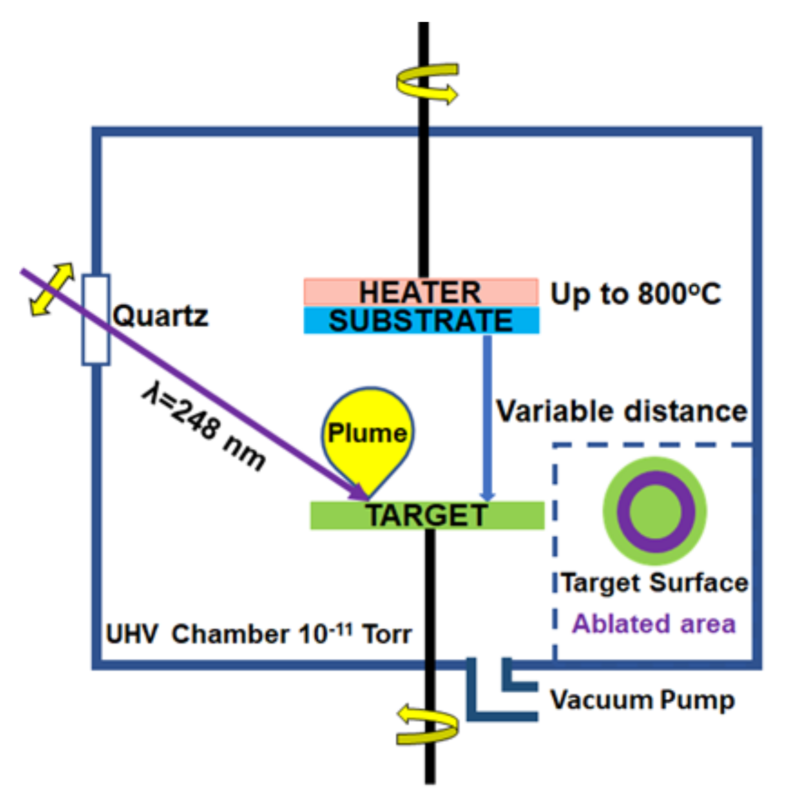
2.1. Pulsed Laser Deposition and Materials

The PLD technique is a versatile research tool that permits the deposition of a broad range of materials [10,11] like complex oxides, high-temperature superconducting coating, polymer, or organic thin films, which can be used in different applications [21,22]. A unique feature of our PLD system is the ability to work at UHV base pressure (8.5 × 10⁻¹¹ Torr) being very useful in controlling unwanted film impurities. Another important feature consists in the laser target manipulator that can accommodate up to four targets of two inches in diameter which are selectable one by one.
There are many parameters which can be tuned for the ablation process, like deposition time, target-substrate distance (dTS), substrate temperature, laser pulse energy, the repetition rate of the laser pulse, laser spot area, speed of rotation targets, and substrates. The depositions of TiO2 thin films on n-Si (100) and of Si on TiO2 were carried out using a KrF excimer laser produced by Coherent-Compex pro 205 F (Coherent Inc., Santa Clara, California, USA) with wavelength (λL = 248 nm), using a pulse duration of 20 ns and at 45° incidence angle to the target. The schematic of the ablation is provided in Figure 1.
During laser ablation, the targets were rotated (10 rpm) and, furthermore, the laser spot was slightly scanned so that fresh surface is exposed to the laser beam during the thin film deposition. The resulting ablation zone on the target surface is shown in Figure 1 inset.
The substrates n-Si (100) were positioned parallel to the target surface at distance dTS. During deposition the substrates were rotated (3 rpm) and heated up 500 °C.
The coupons 10 × 30 mm2 cut from 2 inches n-Si wafer (100) substrate purchased from Merck (Merck KGaA, Darmstadt, Germany), were cleaned in Hydrofluoric Acid (HF, Merck KGaA, Darmstadt, Germany) 10% for 10 min to eliminate the native oxide (SiO2) from the surface, after being ultra-sonicated in acetone and dried under nitrogen flow followed by UHV annealing at 7 × 10⁻⁹ Torr, 600 ℃ for 3 h (SVTA, Eden Prairie, MN, USA). The TiO2 target 99.99% with 5 mm thickness was purchased from Testbourne Ltd. (Hampshire, UK) and as Si target, we used a wafer, 0.5 mm thick, from Merck (Merck KGaA, Darmstadt, Germany). Both targets were 2 inches in diameter.

2.2. Characterization Techniques and Methods

The morphological properties of TiO2 and Si films have been studied using a multimode commercial AFM (SOLVER Next—NT-MDT, Spectrum Instruments, Zelenograd, Moscow, Russia). Cone-shaped tips from monocrystalline silicon (tip radius ~10 nm) on cantilevers with a stiffness of about 34 N/m were used to perform the measurements. The AFM measurements were successfully carried out in tapping mode in which height (topography) signal was acquired.
The sample obtained in optimal conditions was analyzed using a Rigaku SmartLab X-ray Diffractometer (XRD) (Tokyo, Japan) with a copper target (λX = 0.1540598 nm), tube voltage of 45 kV, at 200 mA, and a Kβ filter. The obtained diffractogram was fitted using SmartLab Studio Software from Rigaku (Tokyo, Japan) and compared with existing data from the PDF2 database and scientific articles. The X-ray reflectivity (XRR) measurements on both roughness and thickness of the thin film was performed with the same Rigaku XRD equipment (Tokyo, Japan). The results were obtained using the Integrated Thin Film Analysis Software Global Fit from Rigaku (Tokyo, Japan).
The Woollam M-2000V ellipsometer (J. A. Woollam, Lincoln, Nebraska, USA) was used to evaluate the thickness of the TiO2 buried layer. Ψ and Δ were acquired over the spectral range 550–1000 nm. Measurements were performed at three different angles (55°, 60°, 65°) and the experimental results were processed using a Cauchy mathematical model. The TiO2 thin film with the smoothest oxide surface, in respect with the roughness over the full-length scale, was characterized by means of XRD, XRR, and spectrometric ellipsometry.

3. Results and Discussion

Two endeavors generated this contribution: PLD deposition of a buried TiO2 layer as a part of Si/TiO2/c-Si structure, and the application on the AFM data of an adequate approach to reveal the influence of dTS deposition parameter on the topography of the films. The rough surface profile is determined after each consecutive fabrication of TiO2 and Si film. Finally, the sample obtained at dTS that gives the smoothest oxide layer was analyzed by means of XRD, XRR, and ellipsometry.

3.1. Deposition of the Stacked Si/TiO2 Thin Films on (100) Si Wafer

In order to study the characteristics of the Si/TiO2/n-Si (100) sandwiches structures, the samples were taken out after the TiO2 deposition, and a Ti foil mask was applied to partially cover the surface before the deposition of the top Si layer [9]. Thus, access to both deposited layers was gained for further investigations.
The values of following deposition parameters were considered: substrate temperature 500 ℃, laser pulse energy 500 mJ and the repetition rate of the laser pulse 30 Hz. The surface topography of the deposited TiO2 and Si thin films was investigated for several distances between target and substrate as dTS: 4, 5, and 6 cm.
Before the Si deposition we set up the substrate temperature, then we waited for 3 h for the pressure to reach the lowest value (Pi~10−9 Torr), this being in fact the annealing of the preexisting TiO2 layer in UHV.
In all performed depositions the laser spot was 3 mm2, substrates rotation was 3 RPM and a deposition time of 600 s for each layer.

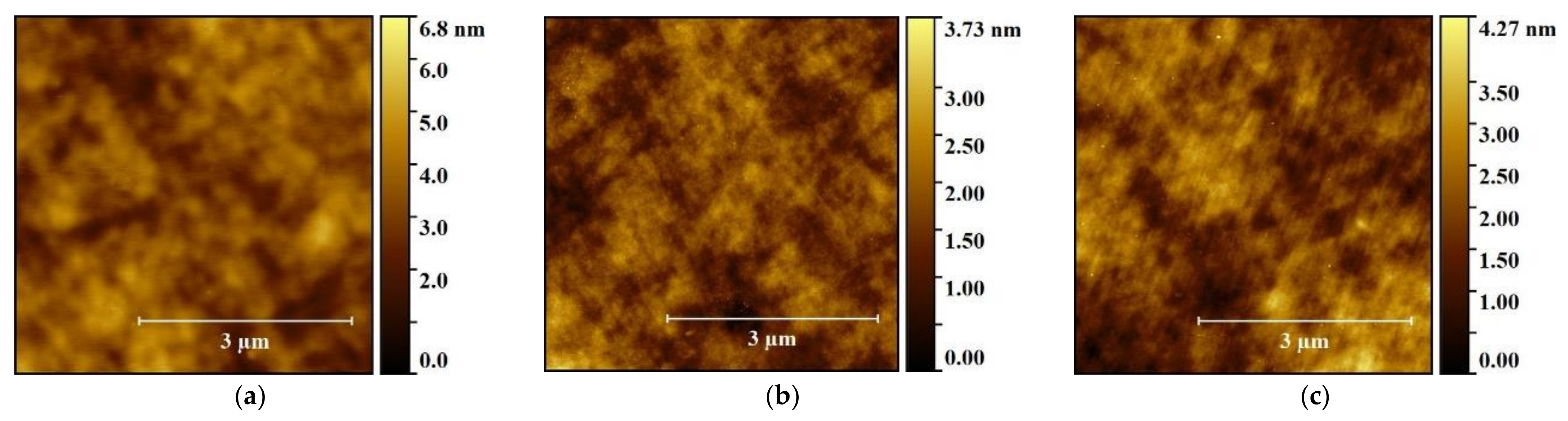
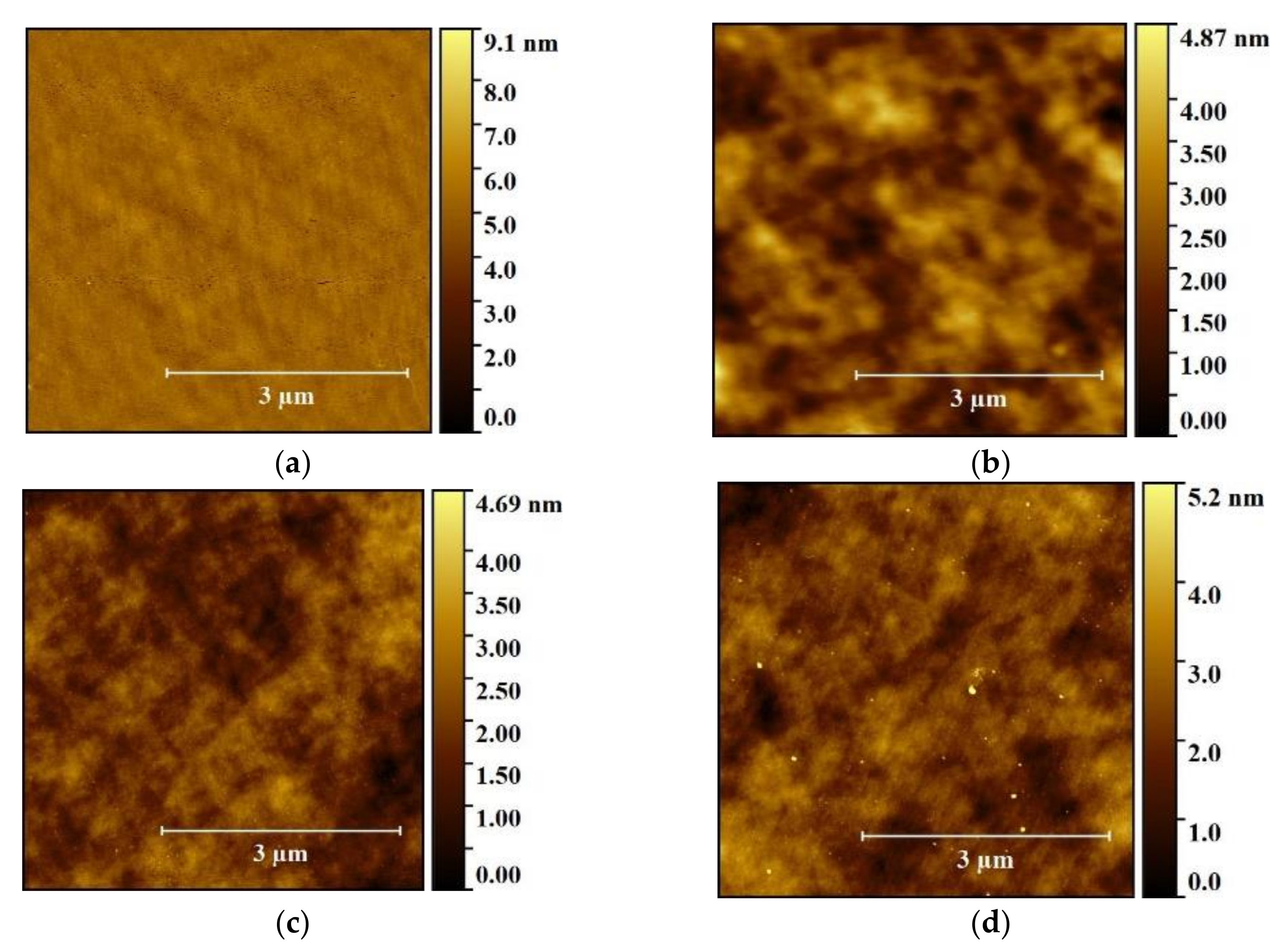
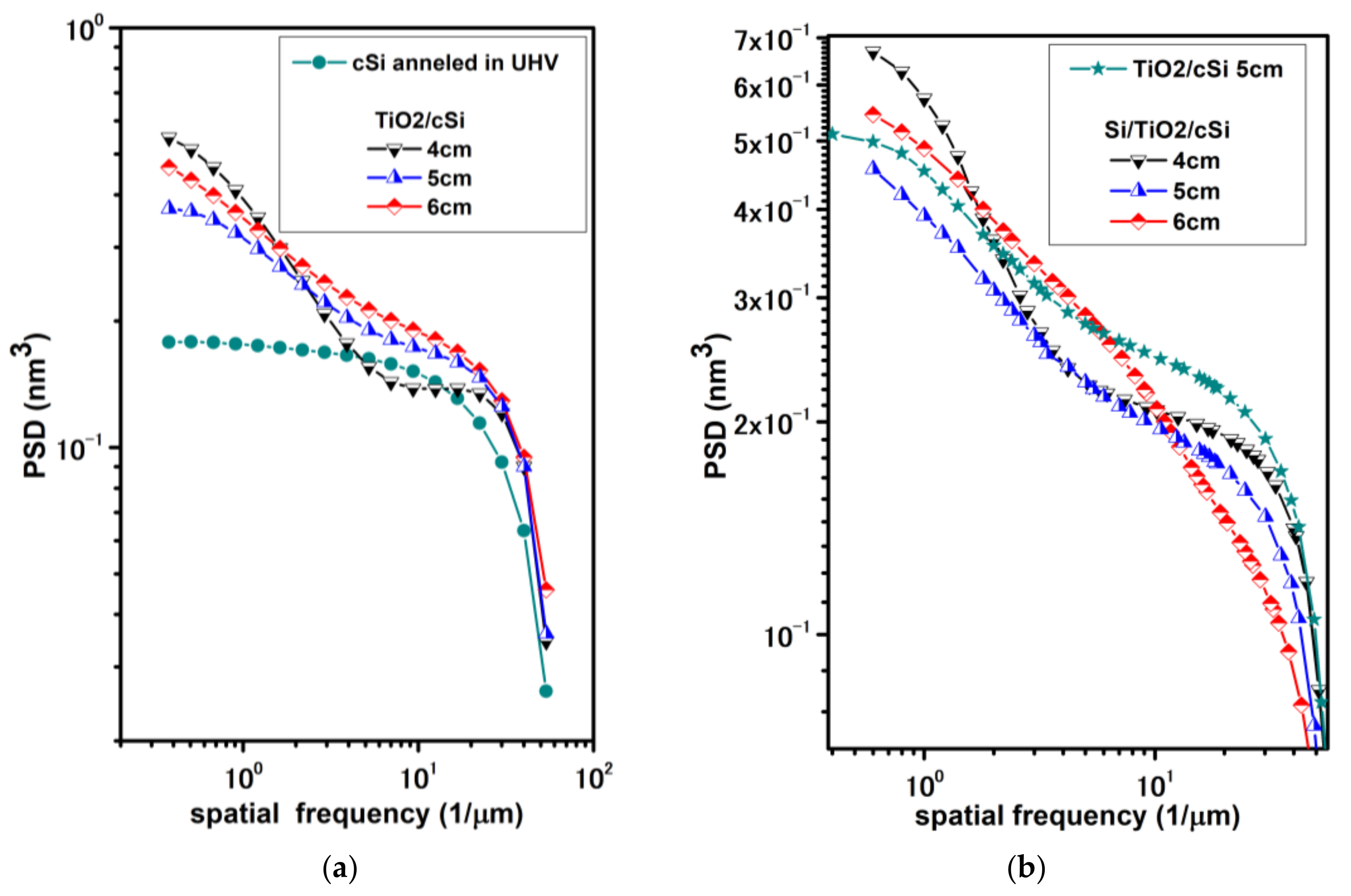
3.2. AFM Characterization of TiO2 and Si Deposited Thin Films on (100) Si Wafer

In this work a special attention was paid to the optimization of the deposited thin films in terms of their surface roughness, which influences their optical and electronic properties.
The Root Mean Square roughness (σRMS) and the Roughness Average (σa) parameters were calculated from the acquired topographic images via an image processing software [23] being given in Table 1.
The AFM topography images recorded on annealed Si wafer (S0), TiO2, and Si thin layers from three different sandwich structures (S1, S2, and S3) corresponding to dTS of 4, 5, and 6 cm are presented in Figure 2 and Figure 3, respectively, all of them revealing a noteworthy uniformity.
The smoothest TiO2 surface is the one deposited at a dTS of 5 cm with a σRMS = 0.37 nm and σa = 0.29 nm. The layers deposited at a dTS of 4 cm and 6 cm, revealed higher surface roughness (Table 1). As it can be seen the Si films showed similar behavior than in the case of oxide films deposition. The smoothest Si surface revealed a σRMS = 0.36 nm and σa = 0.29 nm was obtained for 5 cm dTS.
In Table 1, we show the parameters’ values associated to samples preparation, highlighting the optimal conditions. For each sample the first line corresponds to the fabrication of the TiO2 layer and the second one to the top Si layer. The values in the table correspond to index of sample, dTS, substrate temperature, laser pulse energy, repetition rate of laser pulses, pressure before ablation, pressure during ablation, calculated σRMS, and σa from AFM analysis. As it can be noticed, in all cases, even during ablation, pressure was in UHV interval being lower than 5 × 10⁻⁷ Torr.
According to all the AFM results, the optimal deposition dTS for both type of materials (TiO2 and Si) is dTS = 5 cm (see Table 1, sample S2).

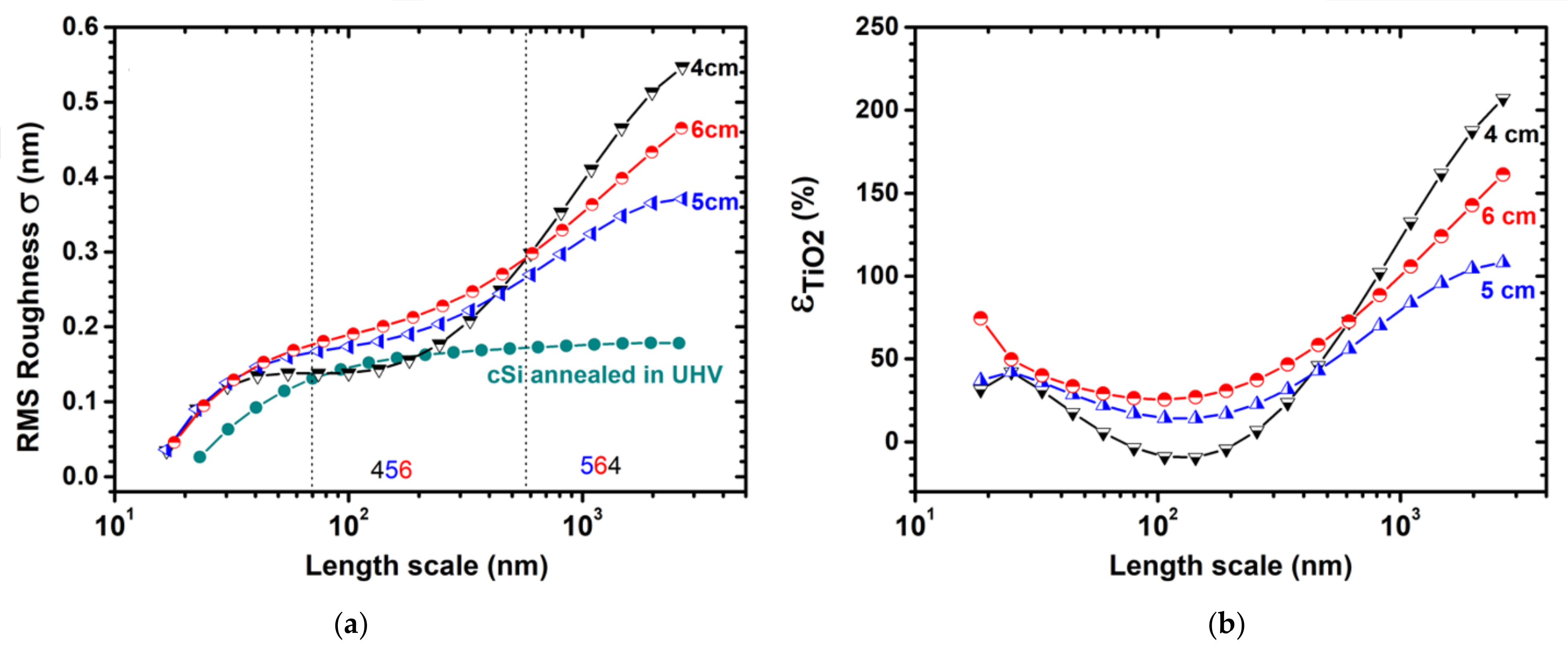
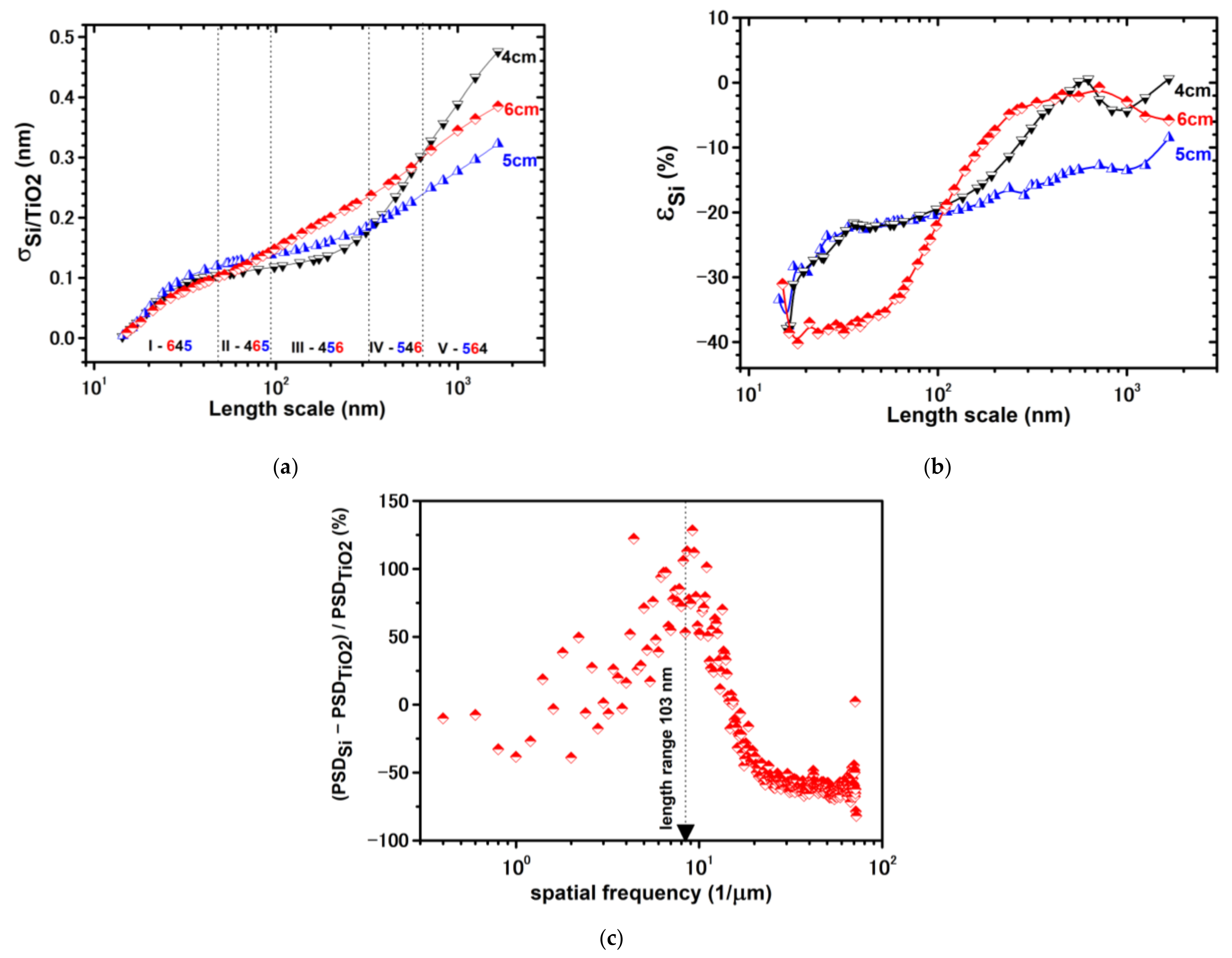
The Roughness Versus the Length-Scale Related to the Target-Substrate Distance

PSD analysis of the AFM images are the most appropriate procedure on revealing the morphological changes on the surface of thin films according to the deposition conditions. The description of sample roughness using σa and σRMS parameters cannot reveal the modifications of the surface features distribution, associated to their sizes and geometry. Samples characterized by almost the same value of σa and σRMS could show very different rough surface profiles, being the signatures of specific growth mechanisms of the thin films. The PSD function is defined for continuous topography data h(x, y) based on Fourier transform (1) [24]:
C 2 D P S D q x , q y = lim L 1 L 2 L 2 L 2 d x L 2 L 2 h x , y e i 2 π x q x + y q y d y 2
where qx and qy are the projection on rectangular axes of spatial frequency; L is the maximum value of x and y. The RMS roughness can be calculated using 2D-PSD function (2):
σ R M S 2 = + C 2 D P S D q x , q y d q x d q y
In the case of isotropic surfaces, the RMS roughness can be expressed by the following relation:
σ R M S 2 = 2 π 0 + C I s o P S D q q d q
where q = (qx2 + qy2)1/2 is the radial spatial frequency [24]. The 1D-PSD function is often used being obtained from 2D isotropic one by imposing to C 1 D P S D to give the same result in (4) as in (3):
σ R M S 2 = 0 + C 1 D P S D q d q ; C I s o P S D = 1 2 π q C 1 D P S D q
The AFM image of the surface is represented by discrete height values h(xi, yj), associated to in plane rectangular coordinates given by Nx and Ny, number of steps on x and y axis respectively. The calculation of the 1D-PSD function (4) in the case of discrete data series is based on changing from integration to summation in the frame of fast Fourier transformation algorithm FFT [25].
These investigations focus on the determination of thin films surface morphology as the contribution of both substrate roughness, and the dTS deposition parameter. Therefore, we search for appropriate ways of using PSD on quantitative determination in terms of roughening to be associated with spectral distribution of frequencies [26].
Figure 4 shows the averaged 1D-PSDs of AFM images collected from the surface of TiO2 and Si films deposited consecutively on (100) Si wafer. The plots correspond to different dTS (4, 5, and 6 cm) inside laser ablation equipment. PSDs diagrams in Figure 4 represent the evolution of surface topography after each deposition from bare crystalline silicon up to the final double stacked layers samples. PSD values calculated from AFM data are given in Figure 4a in the case of TiO2 thin films together with the UHV annealed (100) Si substrate in green, being considered as the reference [27].
Figure 4b gives the PSD data of the same samples, after the Si film deposition onto the previous TiO2 layer. The PSD of the TiO2/c-Si structures in green, was included to indicate the feeble changes of surface morphology after Si thin film deposition, in respect with the case of dTS at 5 cm. Thus, appropriate data analysis has to amplify these differences searching for quantitative determinations.
The surface topography is given first by the deposited species involved in both smoothing and roughing mechanisms associated with the processing conditions as temperature, pressure, laser wavelength, pulse time, and dTS [20]. Moreover, the contribution of the substrate roughness to the deposited film topography, especially at very small thickness, is revealed by the similarities between the coated and uncovered surface. Therefore, the estimation of the direct influences of the dTS on the rough surface profile requires the extraction of the substrate imprinting features into the deposited thin film that could propagate from the interface up to the top of the sample. It means, to determine the changes of the roughness associated to spatial frequency range, determined by the coverage produced by the incoming particles relative to the initial topography. PSD associated to TiO2 and Si films in Figure 4 have been used in the frame of mathematical expression that link the roughness to the spatial frequency or wavelength. We have considered the roughness versus length scale (RLS) function σ(λ; λmin), defined in (5) [24,28].
σ 2 λ ; λ m i n = 1 λ     1 λ m i n C 1 D P S D q d q
where λmin = 1/qmax, it is the parameter associated to the length-scale Δλ = λλmin, with λ representing the spatial wavelength. Λmin has an imposed value of 10 nm, being required to reject the artifacts associated to the radius of the AFM tip used in this study. σ(λ; λmin) has spectral significance being a function that can be defined versus spatial wavelength or spatial frequency. The graphical representations for all data calculated by relation (5) were plotted below using λ on abscissa instead of the length-scale Δλ = λλmin that involve a fixed shift of 10 nm. Moreover, the above RLS function is used to express in percentages the variation of the roughness produced by the deposition of the TiO2 layer relative to that of the c-Si substrate [29].
ε T i O 2 λ = σ T i O 2 λ σ c S i λ σ c S i λ × 100 %
Figure 5a reveals the values of the RLS function on TiO2 thin film, calculated for several values of dTS. The changes of surface roughing by the oxide layer deposition, relative to the initial topography of the (100) Si substrate are shown in Figure 5b according to the relation (6). Titanium dioxide roughness is higher than that of Si wafer for all values of dTS parameter: 4, 5, and 6 cm. These quantitative determinations indicate that for the length-scale associated to 20 nm < λ < 550 nm the smallest roughness is obtained at dTS = 4 cm being almost the same as for Si substrate in between 70 nm and 200 nm. The spatial wavelength λ of the surface features below 550 nm indicates that the local roughing is increasing systematically as the substrate is placed far away from the ablation source as dTS is modified from 4 to 6 cm. This effect corresponds to the diminishing of the incident particles number with orientations at large angles relative to the normal direction towards the substrate. Under these conditions the shadowing process it is expected to contribute on the increasing of roughness [30]. The wide angle distribution of the incoming particles at the smallest dTS distance leads to the conformity of the rough surface profile on top of the deposited TiO2 layer with that of the (100) Si substrate in between 70 and 250 nm.
It is interesting that the smallest values of RLS obtained at 70–550 nm for samples deposited at dTS = 4 cm become greater than the other ones above 600 nm. The contribution of the large features to the overall roughness changes the top of the smoothness above 600 nm in Figure 5a,b. Thus, the best TiO2 sample was obtained at dTS = 5 cm, by considering entire length scale of spatial wavelength into expression (5).
Figure 6 shows the same type of data as those in Figure 5 but for silicon thin film deposited above the previous TiO2 layer. Thus, Figure 6a gives the values of the RLS function associated to Si thin film, calculated for several values of dTS. In this case, the variation of the rough surface profile from that of TiO2 to the on top Si layer ε S i λ is considered relative to that of titanium dioxide film, being this time like a new substrate (7). In this way the initial spectral roughness of the Si-TiO2 interface is related to the surface profile of the on top deposited coverage.
ε S i λ = σ S i λ σ T i O 2 λ σ T i O 2 λ ×   100 % .
The negative values on the vertical axis in Figure 6b of all samples, indicate that silicon deposition on TiO2 produces surface flattening along the full scale of the spatial wavelength.
The expected processes that lead to smoothing is surface migration of silicon atoms by reemission and diffusion, influenced by the oxide coverage. The smoothest samples corresponding to the spatial wavelength between 20 nm and 117 nm was obtained at dTS of 6 cm. Contrary, above the crossing point at 117 nm the same sample turn to the highest roughness of all. Around this value the slope reaches the highest value. It is associated to surface features belonging to size distribution centered close to 8.5 μm−1 as it is revealed by Figure 6c. Here the difference between PSD Si and PSD TiO2 given in Figure 4, divided to PSD TiO2 is plotted versus spatial frequency [26]. The peak corresponds to the length scale of 103 nm being close to the crossing point in Figure 6b.
The silicon films deposited at dTS of 4 and 5 cm have similar dependence versus the length scale up to the crossing point. The smoothest silicon film was obtained at dTS = 5 cm according with the roughness corresponding to entire length scale of spatial wavelength. The above data of the rough surface profile of TiO2 and Si films remain unexplained at the length scale greater than 500 and 100 nm, respectively. Anyway, the interpretation lies on finding the dominant process of the front roughness formation during PLD deposition regarding shadowing, reemission, and surface diffusion [30], by similar investigations.

3.3. Structural and Optical Characterization of TiO2 Thin Films

One goal of this contribution is to build TiO2 layer buried in silicon by PLD consecutive depositions of the oxide and Si films on (100) Si wafer with thickness in the range of tens of nanometer. The improving of the roughness is critical for both interfaces of the buried TiO2 layer in respect with electrical and elastic properties requested for applications in the field of sensors or electronic devices. Complementary techniques as XRD, XRR, and spectrometric ellipsometry were used for the characterization of the smoothest TiO2 layer obtained by laser ablation deposition, according with the optimization of the dTS parameter.

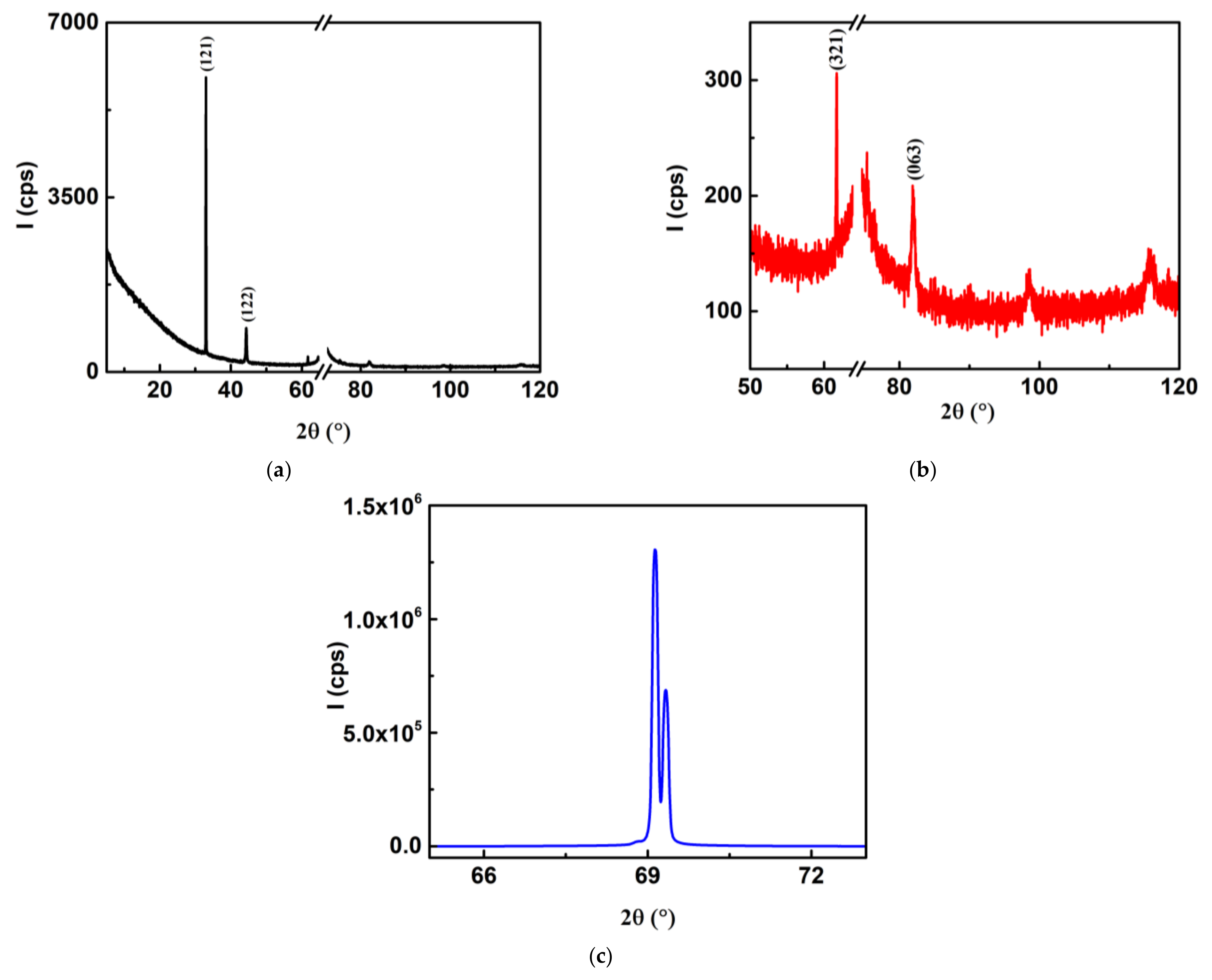
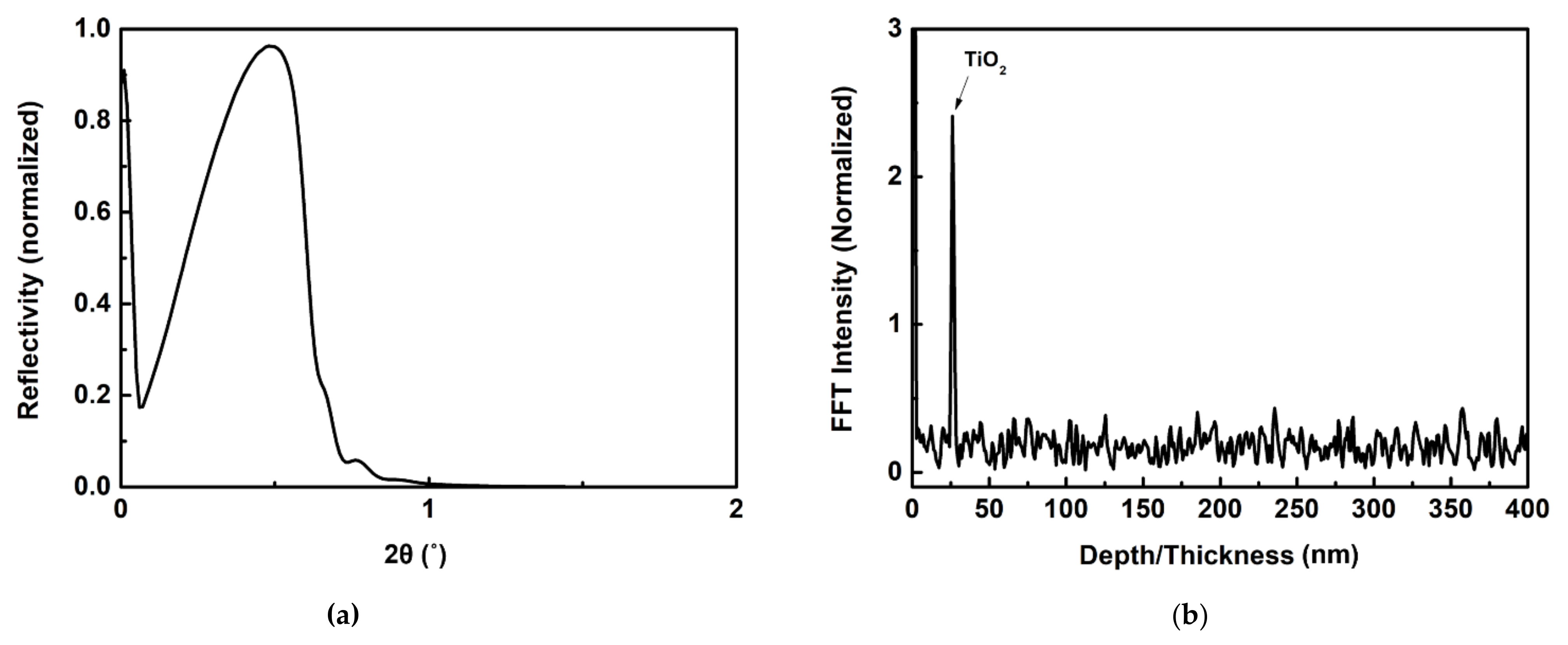
3.3.1. X-ray Diffraction and X-ray Reflectivity
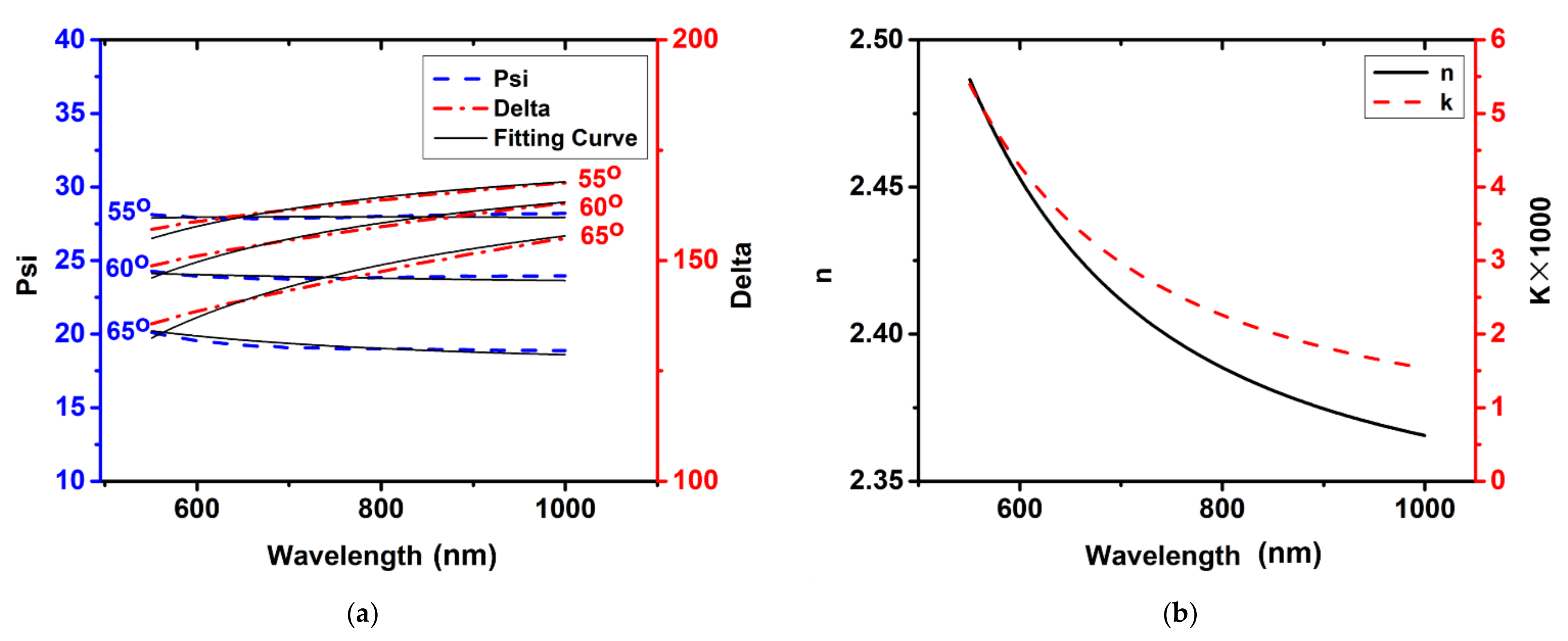
The naturally occurred phases of TiO2 are anatase, rutile, and brookite [31,32,33,34]. The last one is of high importance especially as photocatalysts, due to either oxidative or reductive manifestation of the exposed surface associated to (201) or (210), respectively. Brookite thin films of good quality are much more difficult to be obtained being in a mixture with anatase or rutile [31,35,36]. The XRD diffraction pattern of the TiO2 film in Figure 7 is dominated by (100) Si substrate at 2ϴ = 69.15° [37,38]. The following peaks were associated to brookite phase in the diffractogram presented in Figure 7a: 31.37° (121), 44.93° (122), 63.3° (321), 82.02° (063) with magnification for the last two reflections shown in Figure 7b [31,36,39]. The intense peaks observed at 31.370 and that at 44.93° were reported in reference [31] being associated to brookite phase of PLD deposited films on Si (111) at 750 °C. Furthermore, in [40] are given similar results for ALD (atomic layer deposition) on the same substrate. Brookite-rich thin films of 95% were obtained by PLD after annealing at 290 °C [41]. The above-mentioned reports together with the partial XRD signature shown in Figure 7a,b suggests the formation of the brookite phase into the deposited TiO2 layer. Moreover, the expected peaks of anatase or rutile phase were not identified as other studies reported in the case of deposited TiO2 thin films [31,34]. Unfortunately, the resulted conclusion about the formation of a rich-brookite oxide [39] must be taken with care due to the very thin TiO2 oxide layer combined with the missing of some expected XRD peaks.
X-ray Reflectivity (XRR) was used in order to examine the roughness and the thickness of the TiO2 layer. The roughness determined in the XRR measurement shown in Figure 8a for the TiO2 layer obtained in optimal conditions (sample S2) is 0.37 nm, being in agreement with the AFM data for the same layer (Table 1) [42].
The variation of the X-ray reflectivity shown in Figure 8a is related to the thickness of TiO2 film [43]. The reflectivity oscillation profile (r) is described by the following expression:
r = cos 4 π d λ x sin 2 θ 2 δ ,
where d is the thickness, λx is the wavelength, θ is the incident angle, and δ is the refractive index of X-ray.
The thickness of the layer is given by the peak position in the profile of Fourier transformation with the horizontal axis set as sin 2 θ 2 δ . The thickness of the TiO2 layer was found to be 27 nm as it can be seen in Figure 8b.

3.3.2. Ellipsometry

Optical parameters and the thickness of the thin oxide layer were determined by means of spectroscopic ellipsometry, in order to corroborate with XRR results. The optimal fitting within the Cauchy model of the Ψ and Δ parameters, as it can be seen in Figure 9a, has found the TiO2 layer thickness to be 26.5 nm which is in good agreement with XRR measurement mentioned above. It could be adequate to mention that the variation of thickness relative to the averaged TiO2 and Si thin films thickness are lower than 7.2% and 10.1%, respectively.
The refractive index, namely, its real and imaginary parts, n, k, respectively, that result from the fitting procedure are given in Figure 9b versus the light wavelength. The high value of n and its dependence on the wavelength in Figure 9b is comparable to those reported about rich-brookite TiO2 films [40].

4. Conclusions

This work investigates the profile of the rough surfaces for both TiO2 and Si thin films deposited by PLD on silicon wafer. On top silicon film and the buried oxide layer, enclosed in Si/TiO2/c-Si structures, were prepared for several target-substrate distances dTS, ranging between 4 and 6 cm. We focused on the surface topography in relation with the deposition parameter dTS, and with the initial substrate morphology, considering that at small thickness of the deposited layers their physical properties are more influenced by roughness. The change of dTS value is associated to the modification of angular distribution of the incoming particles on substrate. Therefore, the RLS function associated to PSD-AFM analysis, has been proposed for its sensitivity that gives responses to the evolution of surface topography from bare (100) Si wafer up to on top deposited layer of the Si/TiO2/cSi stacked structure. Thus, the spectral characteristic of the RLS function has the advantage of showing the changes of the roughness versus the length-scale after each deposition, highlighting the influences of the dTS parameter. Furthermore, the topography of the deposited layer results as a combination of the initial roughness of the substrate and the deposition parameter dTS. Relative RLS function takes into account both influences. Thus, we show that the TiO2 deposition on Si(100) produced an increase of the roughness in the range of those features having spatial wavelength greater than 100 nm (Figure 5b). Contrary the Si deposition onto TiO2 determine the smoothing of the initial oxide surface (Figure 6). Thus, the mechanisms of thin films growth can be revealed by adequate AFM data analysis, paving the way to useful physical models that correlate deposition parameters to the features built by particle assembling on surfaces.
In conclusion we show that relative RLS based on PSD function, used for AFM data analysis, reveals quantitatively the evolution of surface profile on top layer of the Si/TiO2/(100) Si stacked films after their consecutive depositions, in relation with both substrate and with the dTS distance.

Author Contributions

Conceptualization, C.C.M., M.B., A.A.M. and M.E.; methodology, C.C.M., M.B., A.A.M. and M.E.; formal analysis, C.C.M., A.P., A.J. and G.V.M.; investigation, C.C.M., A.P., A.J. and G.V.M.; resources, M.E.; data curation, A.P., A.J. and G.V.M.; writing—original draft preparation, C.C.M. and M.B.; writing—review and editing, C.C.M., G.V.M. and M.B.; supervision, M.B., A.A.M. and M.E.; project administration, A.A.M. and M.E.; funding acquisition, M.E. All authors have read and agreed to the published version of the manuscript.

Funding

This work was supported by Romanian Ministry of Research Innovation and Digitalization, Romania, under ECSEL-JU POC 2014-2020 projects: R3-PowerUP Contract no. 1/1.1.3/31.01.2018 Code MySMIS 115833; REACTION Contract no. 4/1.1.3H/24.04.2019 Code MySMIS 121169 and MADEin4 Contract no. 8/1.1.3H/06.01.2020 Code MySMIS 128826.

Institutional Review Board Statement

Not applicable.

Informed Consent Statement

Not applicable.

Data Availability Statement

The data presented in this study are available on request from the corresponding author.

Conflicts of Interest

The authors declare no conflict of interest.

References

  1. Leray, J.-L. Chapter 2: A review of buried oxide structures and SOI technologies. In Instabilities in Silicon Devices; Barbotin, G., Vapaille, A., Eds.; Elsevier: Amsterdam, The Netherlands, 1999; Volume 3, pp. 145–231. [Google Scholar]
  2. Maserjian, J. Single-crystal germanium films by micro-zone melting. Solid-State Electron. 1963, 6, 477–480. [Google Scholar] [CrossRef]
  3. Jastrzebski, L.; Corboy, J.F.; McGinn, J.T.; Pagliaro, R. Growth process of silicon over SiO2 by CVD: Epitaxial lateral overgrowth technique. J. Electrochem. Soc. 1983, 130, 1571–1580. [Google Scholar] [CrossRef]
  4. Izumi, K.; Doken, M.; Ariyoshi, H. C.M.O.S. devices fabricated on buried SiO2 layers formed by oxygen implantation into silicon. Electron. Lett. 1978, 14, 593–594. [Google Scholar] [CrossRef]
  5. Maszara, W.P.; Goetz, G.; Caviglia, A.; McKitterick, J.B. Bonding of silicon wafers for silicon-on-insulator. J. Appl. Phys. 1988, 64, 4943–4950. [Google Scholar] [CrossRef]
  6. Gosele, U.; Reiche, M.; Tong, Q.Y. Properties of SIMOX and bonded SOI material. Microelectron. Eng. 1995, 28, 391–397. [Google Scholar] [CrossRef]
  7. Bruel, M. Silicon on insulator material technology. Electron. Lett. 1995, 31, 1201–1202. [Google Scholar] [CrossRef]
  8. Aspar, B.; Bruel, M.; Moriceau, H.; Maleville, C.; Poumeyrol, T.; Papon, A.M.; Claverie, A.; Benassayag, G.; Auberton-Hervé, A.J.; Barge, T. Basic mechanisms involved in the Smart-Cut® process. Microelectron. Eng. 1997, 36, 233–240. [Google Scholar] [CrossRef]
  9. Moise, C.; Brincoveanu, O.; Katona, A.; Dorobantu, D.; Bojin, D.; Enachescu, M. The study of p-Si/Al2O3/n-Si (100) sandwiches structures deposited by KrF excimer laser ablation. In Proceedings of the 40th-ARA Congress, Montreal, QC, Canada, 28–31 July 2016; Vidu, R., Mindicanu, A., Eds.; ARA Publisher: Montreal, QC, Canada, 2016. [Google Scholar]
  10. Clude, P. (Ed.) Laser Ablation and Its Applications, 1st ed.; Springer: Boston, MA, USA, 2007. [Google Scholar]
  11. Stafe, M.; Marcu, A.; Puscas, N. Pulsed Laser Ablation of Solids–Basics, Theory and Applications, 1st ed.; Springer: Berlin/Heidelberg, Germany, 2014. [Google Scholar]
  12. Linnik, O.; Chorna, N.; Smirnova, N.; Eremenko, A.; Korduban, O.; Stefan, N.; Ristoscu, C.; Socol, G.; Miroiu, M.; Mihailescu, I.N. Pulsed Laser-Deposited TiO2-based Films: Synthesis, Electronic Structure and Photocatalytic Activity. In Semiconductor Photocatalysis–Materials, Mechanisms and Applications, 1st ed.; Cao, W., Ed.; IntechOpen: London, UK, 2016; Volume 1, pp. 135–161. [Google Scholar]
  13. Niilisk, A.; Moppel, M.; Pärs, M.; Sildos, I.; Jantson, T.; Avarmaa, T.; Jaaniso, R.; Aarik, J. Structural study of TiO2 thin films by micro-Raman spectroscopy. Centr. Eur. J. Phys. 2006, 4, 105–116. [Google Scholar] [CrossRef] [Green Version]
  14. Wang, Z.; Helmersson, U.; Käll, P.O. Optical properties of anatase TiO2 thin films prepared by aqueous sol–gel process at low temperature. Thin Solid Film. 2002, 405, 50–54. [Google Scholar] [CrossRef]
  15. Sen, S.; Mahanty, S.; Roy, S.; Heintz, O.; Bourgeois, S.; Chaumont, D. Investigation on sol–gel synthesized Ag-doped TiO2 cermet thin films. Thin Solid Film. 2005, 474, 245–249. [Google Scholar] [CrossRef]
  16. Gyanan, M.S.; Kumar, A. Tunable dielectric properties of TiO2 thin film based MOS systems for application in microelectronics’. Superlattices Microstruct. 2016, 100, 876–885. [Google Scholar] [CrossRef]
  17. Mech, B.C.; Kumar, J. Effect of high-k dielectric on the performance of Si, InAs and CNT FET. Micro Nano Lett. 2017, 12, 624–629. [Google Scholar] [CrossRef]
  18. Moudgil, A.; Singh, S.; Mishra, N.; Mishra, P.; Das, S. MoS2/TiO2 Hybrid Nanostructure-Based Field-Effect Transistor for Highly Sensitive, Selective, and Rapid Detection of Gram-Positive Bacteria. Adv. Mater. Technol. 2020, 5, 1900615. [Google Scholar] [CrossRef]
  19. Ahn, J.-H.; Choi, B.; Choi, S.-J. Understanding the signal amplification in dual-gate FET-based biosensors. J. Appl. Phys. 2020, 128, 184502. [Google Scholar] [CrossRef]
  20. Tang, X.; Bayot, V.; Reckinger, N.; Flandre, D.; Raskin, J.-P.; Dubois, E.; Nysten, B. A Simple Method for Measuring Si-Fin Sidewall Roughness by AFM. IEEE Trans. Nanotechnol. 2009, 8, 611–616. [Google Scholar] [CrossRef]
  21. Abreu Fernandes, S.; Schöps, B.; Nett, R.; Dobbelstein, H.; Stümmler, D.; Ostendorf, A. Laser Ablation of a Thin Film Multilayer for Organic Solar Cells. In Proceedings of the 28th European Photovoltaic Solar Energy Conference and Exhibition (28th EUPVSEC), Paris, France, 30 September–4 October 2013; pp. 2789–2792. [Google Scholar]
  22. Hendel, R. Laser Applications in Solar Cell Manufacturing. Laser Tech. J. 2008, 5, 32–35. [Google Scholar] [CrossRef]
  23. Ulmeanu, M.; Serghei, A.; Mihailescu, I.N.; Budau, P.; Enachescu, M. C–Ni amorphous multilayers studied by atomic force microscopy. Appl. Surf. Sci. 2000, 165, 109–115. [Google Scholar] [CrossRef]
  24. Stover, J.C. Optical Scattering: Measurement and Analysis, 3rd ed.; PM224; SPIE The International Society for Optical Engineering: Bellingham, WA, USA, 2012. [Google Scholar]
  25. Nečas, D.; Klapetek, P. One-dimensional autocorrelation and power spectrum density functions of irregular regions. Ultramicroscopy 2013, 124, 13–19. [Google Scholar] [CrossRef]
  26. Pedreira de Freitas, A.C.; Cardoso Espejo, L.; Brossi Botta, S.; de Sa Teixeira, F.; Aparecida, M.; Cerqueira Luz, A.; Garone-Netto, N.; Bona Matos, A.; Barbosa da Silveira Salvadoril, M.C. AFM analysis of bleaching effect on dental enamel microtopography. Appl. Surf. Sci. 2010, 256, 2915–2919. [Google Scholar] [CrossRef]
  27. Acosta-Alba, P.; Gourdel, C.; Kononchuk, O. Smoothening by Self-Diffusion of Silicon during Annealing in a Rapid Processing Chamber. Solid State Phenom. 2014, 205-206, 364–369. [Google Scholar] [CrossRef]
  28. Singh, R.K.; Holland, O.W.; Narayan, J. Theoretical model for deposition of superconducting thin films using pulsed laser evaporation technique. J. Appl. Phys. 1990, 68, 233. [Google Scholar] [CrossRef]
  29. Berni, M.; Bontempi, M.; Marchiori, G.; Gambardella, A. Roughness conformality during thin films deposition onto rough substrate: A quantitative study. Thin Solid Film. 2020, 709, 138258. [Google Scholar] [CrossRef]
  30. Pelliccione, M.; Lu, T.M. Evolution of Thin Film Morphology–Modeling and Simulations, 1st ed.; Springer: New York, NY, USA, 2008. [Google Scholar]
  31. Moret, M.P.; Zallen, R.; Vijay, D.P.; Desu, S.B. Brookite-rich titania films made by pulsed laser deposition. Thin Solid Film. 2000, 366, 8–10. [Google Scholar] [CrossRef]
  32. Dam, T.; Jena, S.S.; Pradhan, D.K. Equilibrium state of anatase to rutile transformation for nano-structured Titanium Dioxide powder using polymer template method. In Proceedings of the IOP Conference Series: Materials Science and Engineering 5th National Conference on Processing and Characterization of Materials, Rourkela, India, 12–13 December 2015. [Google Scholar]
  33. Coronado, D.R.; Gattorno, G.R.; Pesqueira, M.E.E.; Cab, C.; de Coss, R.; Oskam, G. Phase-pure TiO2 nanoparticles: Anatase, brookite and rutile. Nanotechnology 2008, 19, 145605. [Google Scholar] [CrossRef] [PubMed]
  34. Zhao, B.; Chen, F.; Huanga, Q.; Zhanga, J. Brookite TiO2 nanoflowers. Chem. Commun. 2009, 34, 5115–5117. [Google Scholar] [CrossRef]
  35. Nechache, R.; Nicklaus, M.; Diffalah, N.; Ruediger, A.; Rosei, F. Pulsed laser deposition growth of rutile TiO2 nanowires on Silicon substrates. Appl. Surf. Sci. 2014, 313, 4852. [Google Scholar] [CrossRef]
  36. Bokhimi, X.; Pedraza, F. Characterization of brookite and a new corundum-like titania phase synthesized under hydrothermal conditions. J. Solid State Chem. 2004, 177, 2456–2463. [Google Scholar] [CrossRef]
  37. Zhao, Q.; Xu, J.; Xu, X.Y.; Wang, Z.; Yua, D.P. Field emission from AlN nanoneedle arrays. Appl. Phys. Lett. 2004, 85, 5331. [Google Scholar] [CrossRef]
  38. Hullavarad, S.; Hullavarad, N.; Look, D.; Claflin, B. Persistent Photoconductivity Studies in Nanostructured ZnO UV Sensors. Nanoscale Res. Lett. 2009, 4, 1421. [Google Scholar] [CrossRef] [PubMed] [Green Version]
  39. ICDD. PDF-4 Database, International Centre for Diffraction Data; ICDD: Newtown Square, PA, USA, 2018. [Google Scholar]
  40. Qaid, S.M.H.; Hussain, M.; Hezam, M.; Khan, M.A.M.; Albrithen, H.; Ghaithan, H.M.; Aldwayyan, A.S. Structural and optical investigation of brookite TiO2 thin films grown by atomic layer deposition on Si (111) substrates. Mater. Chem. Phys. 2019, 225, 55–59. [Google Scholar] [CrossRef]
  41. Haggerty, J.E.S.; Schelhas, L.T.; Kitchaev, D.A.; Mangum, J.S.; Garten, L.M.; Sun, W.; Stone, K.H.; Perkins, J.D.; Toney, M.F.; Ceder, G.; et al. High-fraction brookite flms from amorphous precursors. Nat. Sci. Rep. 2017, 7, 15232. [Google Scholar] [CrossRef] [PubMed]
  42. Su, H.-C.; Lee, C.-H.; Lin, M.-Z.; Huang, T.-W. A Comparison Between X-ray Reflectivity and Atomic Force Microscopy on the Characterization of a Surface Roughness. Chin. J. Phys. 2012, 50, 291–300. [Google Scholar]
  43. McDaniel, M.D.; Posadas, A.; Wang, T.; Demkov, A.A.; Ekerdt, J.G. Growth and characterization of epitaxial anatase TiO2(001) on SrTiO3-buffered Si (001) using atomic layer deposition. Thin Solid Film. 2012, 520, 6525–6530. [Google Scholar] [CrossRef]
Figure 1. Schematics of the laser ablation (PLD) process.
Coatings 11 01350 g001
Figure 2. 5 × 5 µm2 2D AFM topography images of (a) annealed silicon wafer S0; TiO2 thin films: (b) S1; (c) S2; (d) S3 sample, respectively.
Coatings 11 01350 g002
Figure 3. 5 × 5 µm2 2D AFM topography images of Si thin films: (a) S1; (b) S2; (c) S3 sample, respectively.
Coatings 11 01350 g003
Figure 4. (a) The PSD function of TiO2 thin films deposited on crystalline silicon (c-Si) substrate (green) at different dTS of 4, 5, and 6 cm. (b) The PSD of Si film deposited onto previous TiO2 layer at the same dTS values. PSD of TiO2/c-Si structure considered as substrate for Si layer deposition at dTS = 5 cm (green) is given to reveal the changes on surface topography of the prepared samples.
Coatings 11 01350 g004
Figure 5. (a) TiO2 thin film roughness calculated using radial PSD versus the length scale corresponding to dTS of 4, 5, and 6 cm. The c-Si substrate roughness is represented in dark green. (b) TiO2 thin film roughness variation relative to (100) Si substrate for the same dTS values, versus the length scale.
Coatings 11 01350 g005
Figure 6. (a) Si thin film RMS roughness versus the length scale at different values of dTS. (b) The relative roughness variation between Si and TiO2 thin film surfaces, the last being the substrate coverage of the second layer deposition. The highest slope found in the case of the sample prepared at dTS = 6 cm, close to the crossing point, corresponds to surface features distribution peak at 8.5 μm−1 shown in (c) that gives the relative variation of PSD amplitude of silicon layer relative to TiO2 thin film acting as substrate coverage.
Coatings 11 01350 g006
Figure 7. (a) XRD Diffractogram of TiO2 layer (sample S2) in the range 5–120°, showing the specific peaks of brookite, (b) zoom in, (c) the peak of the Si (100) substrate.
Coatings 11 01350 g007
Figure 8. (a) X-ray reflectivity curve of TiO2 on n-Si (100). (b) The Fourier transform profile of the reflectivity curve.
Coatings 11 01350 g008
Figure 9. (a) Fitting of ellipsometry results Ψ and Δ for 3 measuring angles, (b) optical constants for TiO2 layer used for fitting.
Coatings 11 01350 g009
Table 1. The deposition parameters as: substrate temperature, laser power and pulse frequency, pressure before and during films deposition, and the corresponding σRMS and σa roughness calculated for the 2D topography images recorded for TiO2 and Si thin films (5 × 5 µm2).
Deposition ParametersAFM
Analysis
SampleDeposited Thin FilmdTS (cm)T (°C)E (mJ)RR (Hz)Pi (Torr)Pa (Torr)σRMS (nm) σa (nm)
S0Si waferxxxxxx0.21 ± 0.0260.19 ± 0.023
S1TiO24500500306.7 × 10−94.2 × 10−70.58 ± 0.0980.46 ± 0.083
Si4500500307.6 × 10−90.9 × 10−70.58 ± 0.0770.44 ± 0.040
S2TiO25500500305.8 × 10−94.8 × 10−70.37 ± 0.0630.29 ± 0.048
Si5500500303.9 × 10−91.0 × 10−70.36 ± 0.0240.29 ± 0.018
S3TiO26500500306.0 × 10−94.2 × 10−70.46 ± 0.0240.35 ± 0.023
Si6500500302.2 × 10−95.0 × 10−80.48 ± 0.0900.32 ± 0.058
Publisher’s Note: MDPI stays neutral with regard to jurisdictional claims in published maps and institutional affiliations.

