Article

Design and Preparation of Nanoporous Cu/Ag Multilayer Films

1
State Key Laboratory of Nuclear Physics and Technology, School of Physics, Peking University, Beijing 100871, China
2
College of New Energy and Materials, China University of Petroleum, Beijing 102249, China
3
School of Materials Science and Engineering, Hefei University of Technology, Hefei 230009, China
*
Authors to whom correspondence should be addressed.
Coatings 2021, 11(10), 1187; https://doi.org/10.3390/coatings11101187
Submission received: 31 August 2021 / Revised: 21 September 2021 / Accepted: 24 September 2021 / Published: 29 September 2021
(This article belongs to the Special Issue Nanoporous Films)

Abstract

:
Cu30Al70 and Ag30Al70 multilayer precursor films were prepared by magnetron sputtering, respectively. Then the nanoporous Cu/Ag multilayer composite films were successfully prepared by selecting the appropriate H2SO4 solution as the dealloying solution. It was found that the nanoporous structure was stable in the dealloying solution. The morphology and structure of nanoporous multilayer films are mainly related to the phase composition of precursors. The structure of nanoporous multilayers can be simply regarded as the superposition of single-layer structures. Our work shows that nanoporous multilayers can be well-prepared by magnetron sputtering combined with dealloying.

1. Introduction

Structural materials used in advanced nuclear reactors are required to endure neutron irradiation up to several hundred displacements-per-atom (dpa). The residual defects induced by high-density irradiation lead to the change of the microstructure of the material and then degrade its mechanical properties [1,2]. It is a common and effective method to improve the radiation resistance of materials by introducing various types of defect sinks to absorb the defects produced by irradiation and thus reduce the defect concentration [3,4]. Dislocation networks [5,6], grain boundaries [7], twin boundaries [8,9], phase boundaries [10], free surfaces [11], small precipitates [12] and voids [13] can be used as defect sinks. Oxide dispersion strengthened (ODS) steels are typical radiation-damage-resistant materials designed with a large number of grain boundaries, phase boundaries and precipitates, and have excellent high temperature creep resistance and chemical stability [14]. Nanocrystals have abundant grain boundaries, which effectively reduce the size and density of defect clusters and the density of helium bubbles (He) [15,16,17].
Nanoscale metallic multilayer films, which have higher radiation tolerance than the counterpart, are generally composed of different metal layers alternately [18,19,20]. With the decrease of individual layer thickness, the volume fraction of interfacial area increases, and thus the absorption sinks of radiation-induced defects increase and the radiation resistance of materials increases [21]. Nanoscale multilayer films with desired mechanical, electrical, optical and magnetic properties can be tailored by adjusting the interface type, density and film thickness [22,23,24,25]. Chen et al. prepared two types of Cu/Fe multilayers with incoherent interface of face-centered cubic/body-centered cubic (FCC/BCC) structure and coherent interface (FCC/FCC) on single crystal Si substrate by magnetron sputtering, respectively [26]. The results showed that these two different types of interfaces can effectively reduce the irradiation damage. The incoherent interface was stable and clear, and the He bubble density was significantly reduced after irradiation. The coherent interface greatly reduced the average size of He bubbles and reduced the irradiation swelling as well, indicating the coherent multilayer film is also an excellent irradiation-resistant material. However, the improvement of radiation resistance of multilayer films is limited as it depends only on the interfaces as the defect sinks. Wang et al. [27] prepared Cu/Ag multilayers with FCC/FCC structure by accumulative roll bonding (ARB) approach. Their work showed that although multilayer interfaces are still in high density, they appear to be somewhat insufficient to heal the radiation-induced vacancies and interstitials.
Nanoporous (NP) metals have the characteristics of both metal and porous materials, and have been studied in catalysts [28], energy storage [29] and surface-enhanced Raman scattering substrates [30]. Dealloying has been widely used in the preparation of various NP metal materials because of its simple process, low cost and easy control. Melt spinning and arc melting are the most commonly used methods to prepare precursors [29,31]. The preparation of precursors by magnetron sputtering has been extensively studied [32]. The previous studies showed that abundant free surface of NP metals can be used as both defect absorption sinks and gas-atom release sites, indicating an irradiation resistance potential [32,33]. Sun et al. prepared precursor Ag23Cu77 film by magnetron sputtering and then obtained NP-Ag by dealloying. In situ observation showed that the irradiation-induced SFTs, dislocation loops and dislocation segments were removed by the free surface in NP-Ag [34].
As the nanoscale multilayer material has large volume fraction of interfacial area and nanoporous material has plenty of free surface, we speculate that integrating these two materials may further improve the radiation damage resistance of the materials. Magnetron sputtering is not only a convenient method to prepare multilayer films, but also an effective method to prepare NP precursors. It is expected to successfully prepare nanoporous multilayers with both multilayer phase interface and free surface. Other precursor preparation methods are difficult to prepare multilayer structures. In addition, the magnetron sputtering technology is easy to operate, the film thickness is accurately controlled, and the element type and proportion can be adjusted at will, making it easier to achieve the design purpose. We have shown the possibility of preparing bilayer nanoporous copper films in our previous work [11]. Au, Pt, Pb, Ag and Cu are the most common metals with nanoporous structure prepared by dealloying. Compared with other elements, Ag and Cu have great cost advantages in experiment and practical application. Secondly, Ag and Cu are immiscible, and the multilayer structure will have stable layer interfaces. Finally, the precursors commonly used to prepare nanoporous Ag and Cu are Ag-Al and Cu-Al respectively, which have the same active element Al, which is conducive to the selection of dealloying solution [35,36,37].
In this study, the precursor films of Ag-Al and Cu-Al were prepared by magnetron co-sputtering. NP-Ag and NP-Cu films were prepared by dealloying in the H2SO4 solution, respectively. On this basis, Ag-Al/Cu-Al bilayers and multilayer precursor films were successfully prepared, and NP-Cu/Ag bilayers and multilayer films were obtained by dealloying.

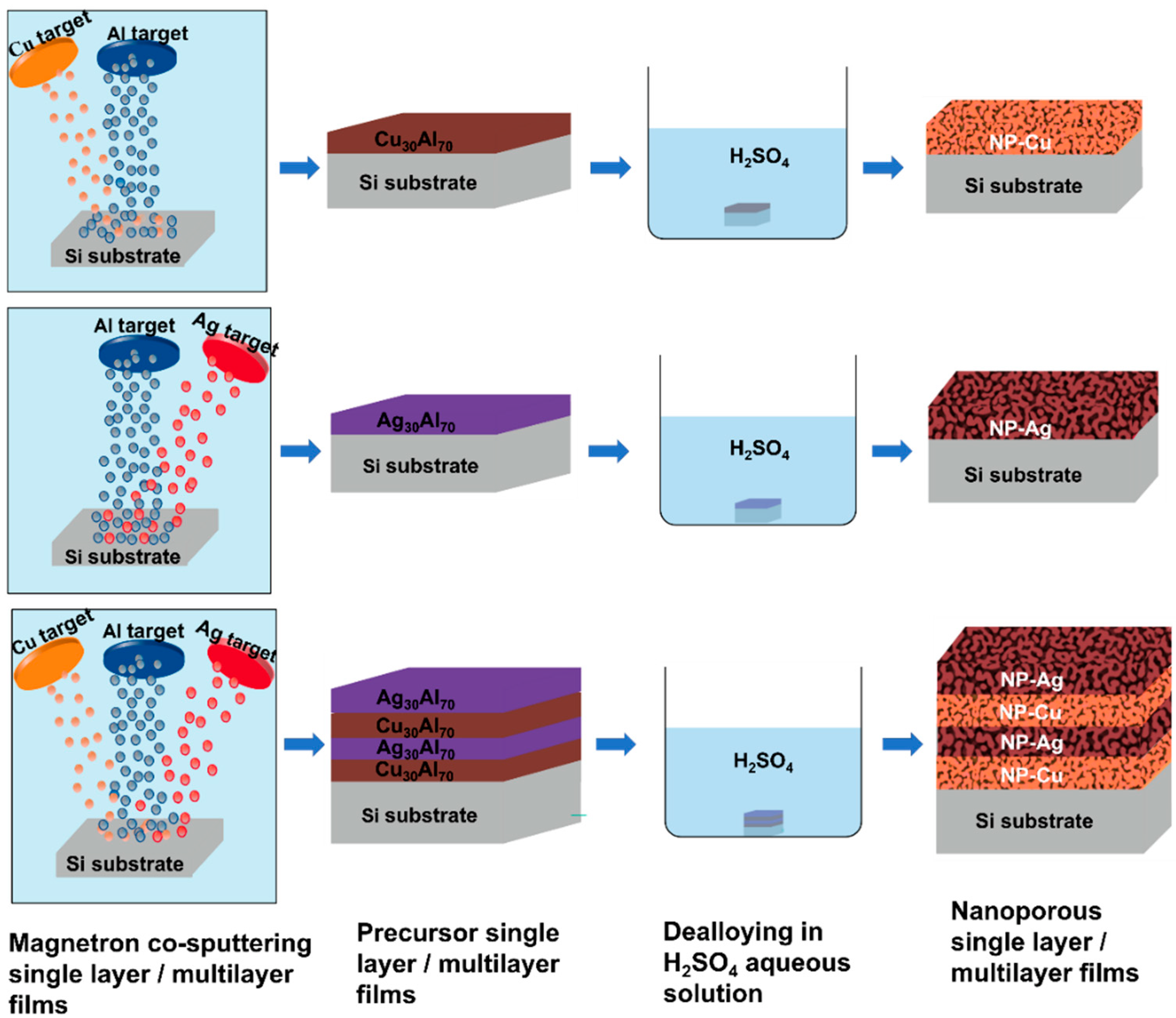
2. Materials and Methods

Cu-Al and Ag-Al alloy precursor films were prepared on Si (100) substrates by magnetron co-sputtering. The target materials used in the experiment were Cu target (99.99%), Ag target (99.99%), Al target (99.99%) and Cr target (99.99%) (Beijing Goodwill Metal Technology Co., Ltd., Beijing, China). Cr target was used to deposit Cr thin film as a buffer layer to enhance the adhesion between the films and the substrate. The Si substrates were cleaned successively with hydrofluoric acid solution and anhydrous ethanol prior to deposition to remove the oxides and dust on the substrate surfaces and keep the surfaces clean. Before deposition, the base pressure of reaction chamber was lower than 1 × 10⁻⁴ Pa. Argon was kept flowing into the chamber at a flow rate of 50 sccm, and the argon partial pressure was kept at 1.8 Pa. The substrates were rotated at the speed of 20 rpm to ensure the homogeneity of the thin films in an area of 6 cm in diameter. The substrate temperature was kept at ambient temperature during sputtering.
Cu30Al70 and Ag30Al70 alloy precursor films with thickness of about 600 nm were deposited on the substrate by adjusting the power of the target and the deposition rate to control the composition of the films. The thickness of films was measured by the Bruker Dektak-XT (Bruker, Madison, WI, USA) stylus profiling system. An RF source was selected for Cu target and Ag target, respectively, and the DC source was selected for Al target, so that Cu target and Al target could be co-sputtered at the same time, and Ag target and Al target could be co-sputtered at the same time. The RF power of Cu target was 100 W, the RF power of Ag target was 45 W, and the DC power of Al target was 300 W. The deposition rate for Cu film and Ag film was 0.1 nm/s and for Al target was 0.3 nm/s. The deposition rate was obtained by measuring the thickness of thin film deposited at certain time. The deposition time for single-layer precursor was 25 min and for multilayer precursor was 55 min. The distance and the angle between target and substrate were 105 mm and 30°, respectively.
Energy Dispersive X-ray spectroscopy (EDS) measurements confirmed that the element composition of the precursor films was consistent with the requirements of our design. In addition, Cu30Al70/Ag30Al70 multilayer precursor films with a total thickness of about 1.3 μm were prepared after 55 min under the same conditions.
The dealloying of all the alloy precursor films was carried out in 2 M H2SO4 aqueous solution at room temperature at different times. The reaction vessel was sealed during dealloying. When reaching the desired etching time, the samples were taken out and rinsed in ultrapure water and absolute ethanol for three to four times to remove the residual sulfuric acid, and then dried with a nitrogen gun. All dealloying experiments were carried out in the fume hood. The samples preparation process is illustrated in Figure 1.
The microstructures and the thickness of the as-deposited and as-dealloyed films were characterized by scanning electron microscopy (SEM) using FEI NanoSEM 430 microscope (FEI, Hillsboro, OR, USA) operating at 15 kV. The phases of the films before and after dealloying were identified by X-ray diffraction (XRD) (PANalytical, Almelo, The Netherlands) using a Cu Kα radiation on a PANalytical Empyrean. The grazing incidence mode was selected and the incidence angle was set to 1.5°. The element composition and distribution of the films were performed by energy dispersive X-ray spectroscopy (EDS) on FEI NanoSEM 430. The grain sizes of the precursor films were measured by a program, Nanomeasure. The morphologies of the NP films were characterized by analysis of plane SEM images taken from surfaces by Automatic Quantitative Analysis of Microscopy Images (AQUAMI) [38].

3. Results and Discussion

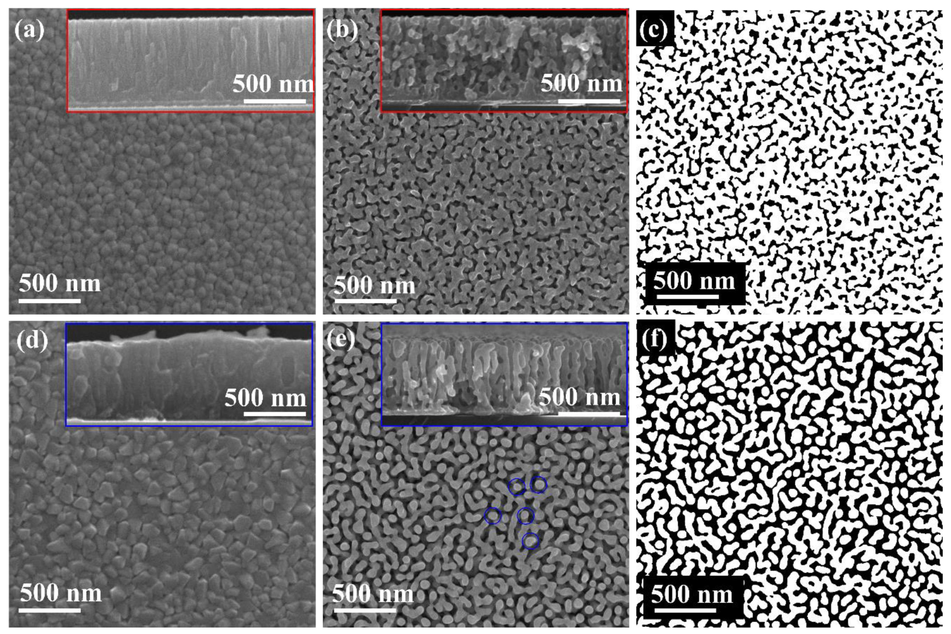
3.1. Preparation of Single Layer NP-Cu and NP-Ag Films

It is well known that dealloying solution will affect the porous structure and ligament size of NP metals. For NP-Cu/Ag multilayer structure, it is critical to design the optimal type, concentration and corrosion time of dealloying solution so that each layer of precursor can form NP structure. High stability of each layer in dealloying solution is another requirement.
In most experiments, NP-Ag was prepared by etching Ag-Al precursor in HCl solution [36,37,39]. However, the halogen anions contained in HCl acid solution can accelerate the diffusion of noble elements and coarsen the ligaments of NP materials [35]. In our previous work, we found that HCl solution corrodes Ag-Al precursors to form coral structure rather than porous structure. Therefore, HCl solution was not suitable for our sample system. NP-Cu is usually prepared by dealloying Cu-Al precursors with NaOH solution [35]. However, Ag-Al alloy (Ag content of 15–50 atom%) cannot be completely dealloyed in NaOH solution and many cracks appear [39]. Therefore, NaOH solution could not be used. The results show that both Ag-Al and Cu-Al precursors can be mildly dealloyed and form a typical NP structure in the H2SO4 solution without halogen anions. Therefore, 2 M H2SO4 was selected as the dealloying solution.
Figure 2a,d shows the plan-view SEM images of as-deposited Cu30Al70 and Ag30Al70 precursor thin films. Their cross-sectional SEM images are shown in the insets in Figure 2a,d, respectively. Figure 2a,d shows that the surfaces of the two films are flat without holes and cracks. The structure of Cu30Al70 film (Figure 2a) grows into columnar grains with a high aspect ratio, and the in-plane grains are relatively smooth polygons. This is because Cu and Al co-sputtering reduces atomic mobility, and the anisotropy of nucleation energy and growth rate leads to film coalescence and thickening [40]. The statistical grain size is 59 ± 14 nm.
As-deposited Ag30Al70 film (Figure 2d) is mainly composed of small granular and columnar morphology. The granular structure on the surface of the film is polygonal with sharp edges. This is consistent with the two-dimensional growth structure where Ag and Al atoms are approximately infinite surface diffusion, in which the new crystal nucleates periodically on the surface of the growing crystal [41]. It is also observed from the cross-sectional view that the edge surface of Ag30Al70 film is coarser than that of Cu30Al70 film.
Figure 2b,e shows the plan-view SEM images of NP Cu and NP Ag after dealloying Cu30Al70 and Ag30Al70 precursor films, respectively. Their corresponding cross-sectional SEM images are shown in the insets in Figure 2b,e, respectively. Both NP films were prepared by dealloyed in 2 M H2SO4 solution at room temperature. NP-Cu films were dealloyed for 130 min and NP-Ag films for 240 min. The details to choose the appropriate dealloying time for preparing NP-Cu and NP-Ag can be found elsewhere [42]. The results show that both NP-Cu and NP-Ag films have uniform and open three-dimensional continuous interpenetrating ligaments and nanopore structures.
AQUAMI software extracts the information of SEM images and then automatically segments, measures and analyzes them. Figure 2c,f is the bright and dark segmentation mask images after AQUAMI treatment for Figure 2b,e, respectively. The darker phase is the pore space. NP-Cu films formed isotropic nano pore structure, with average ligament size of 46 ± 16 nm, average pore size of 24 ± 8 nm and surface areal porosity of about 26%. NP Ag film forms a partial anisotropic channel nanopore structure. Figure 2e of plan-view SEM shows that there are many independent single circular ligament tips (e.g., as shown in the blue circle). The average ligament size is 47 ± 13 nm, the average pore size is 31 ± 12 nm, and the surface areal porosity is about 44%. We speculate that the rapid diffusion and recombination of Ag makes the NP Ag membrane retain the columnar structure of some precursor membranes.

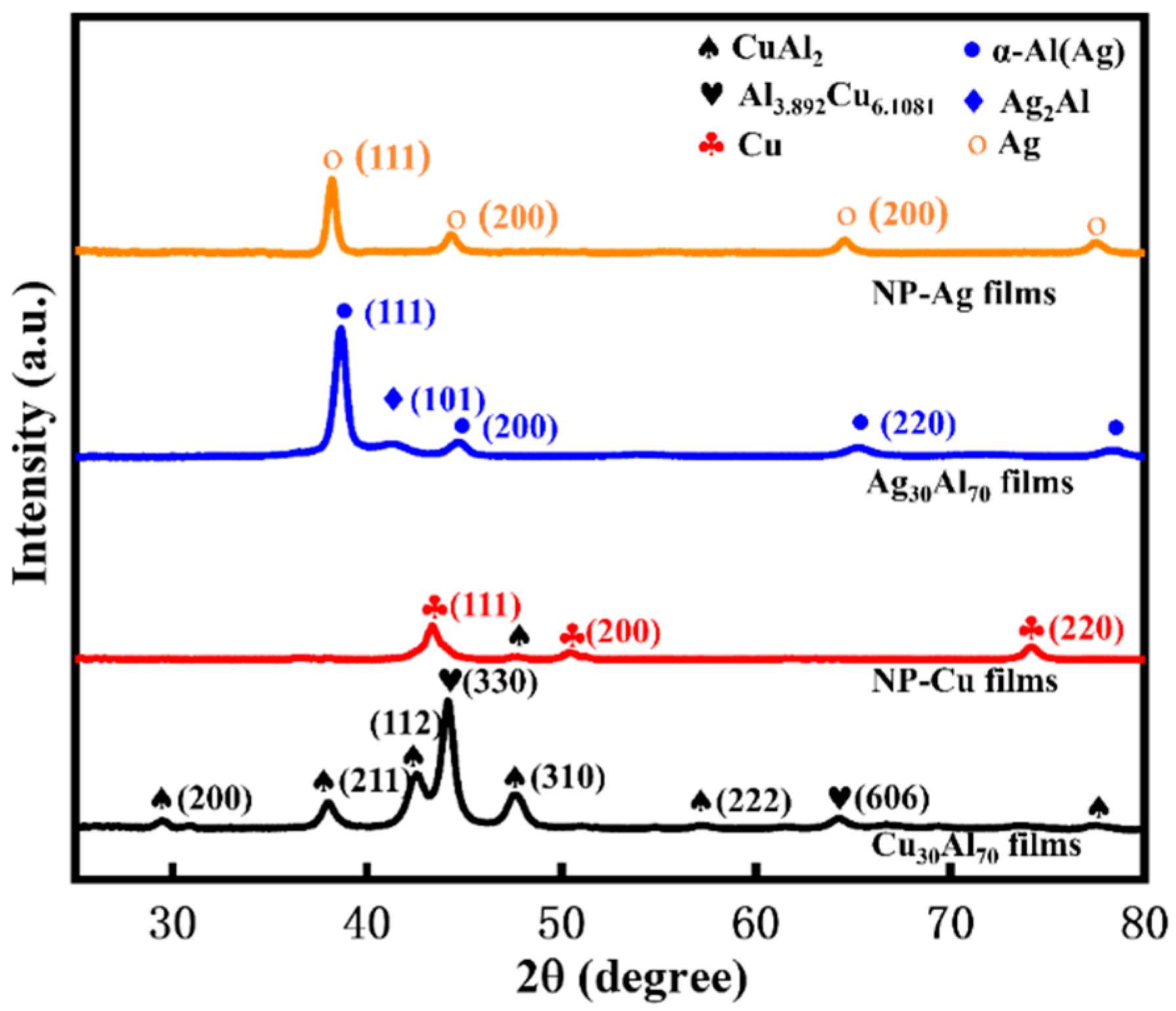
3.2. Phase Composition of Monolayer Precursor Films Cu30Al70 and Ag30Al70 and Monolayer NP-Cu and NP-Ag Films

In order to study the changes of phase structure before and after dealloying, XRD was used to characterize the phase structure through small angle grazing incidence. For thin film materials, the grazing incidence mode can increase the detection path of X-ray in the thin film materials, obtain more film information and avoid the peak position of single crystal Si substrate. Figure 3 shows the XRD diffraction patterns of as-deposited Cu30Al70 and Ag30Al70 precursor films and NP-Cu and NP-Ag films, respectively. The phase identification was carried out by HighScore software (version 4.7). The results illustrate that two phases were observed in Cu30Al70 precursor films: Al3.892Cu6.1081 phase with Rhombohedral structure (represented by R (hkl)) and Al2Cu phase with Tetragonal structure (represented by T(hkl)). The diffraction peaks R (330), R (606), T (200), T (211), T (112), T (310) and T (222) can be seen obviously. After dealloying, NP-Cu films are mainly composed of Cu phase. All the peaks of Al3.892Cu6.1081 disappear. The peak at 47.62 degrees of Al2Cu still exists, indicating that there is still a small amount of CuAl2 phase, and some Al atoms exist in NP-Cu film. But it has little effect on the shape and structure of NP-Cu.
Combined with the diffraction peak intensity, two phases were observed in the Ag30Al70 precursor film: the solid solution with FCC structure (represented by F (hkl)) α-Al (Ag) phase and intermetallic phase Ag2Al with Hexagonal structure (represented by H (hkl)). The diffraction peaks of F (111), F (200), F (220) and H (101) are obvious. Solid solution α-Al (Ag) phase is the main phase, and intermetallic phase Ag2Al has a small amount. After dealloying, NP-Ag films have a single Ag phase. Since all element Al in NP-Ag is dissolved, the porosity of NP-Ag films is higher than that of NP-Cu films.
The structural differences between NP-Cu films and NP-Ag films are mainly reflected in these three points: Firstly, the ligament size of the two NP films is almost the same, but the pore size and porosity of NP-Ag films are much larger than that of the NP-Cu membrane. Secondly, the ligaments of NP-Ag films are long and the surface looks smooth, while the ligaments of NP-Cu films seem to be unable to count the length and the surface is rough. Finally, the cross-sectional SEM image shows that the pore structure of the NP-Cu film is isotropic, while NP-Ag exhibits anisotropic channel pore structure.
The structure of NP films is largely related to the crystal structure and phase composition of precursors. In this study, the precursor Cu30Al70 films have an obvious anisotropic columnar structure, while the nanopores of the dealloyed NP-Cu films are uniform and isotropic. The precursor Ag30Al70 films are mainly composed of small particles, but the NP-Ag films show anisotropic channel pore structure. The nanopore structure of these two NP films is not related to the crystal structure of the precursor, so we believe that the phase composition of the precursor is the main factor affecting the structure of NP films. In the process of dealloying, NP-Cu films always contain Al2Cu phase, which affects the diffusion and migration of Cu, resulting in rough ligament surface. Moreover, since some Al atoms remaining in NP-Cu will occupy part of the volume, NP-Cu in Figure 2b has smaller pore size and lower surface porosity. The precursor Ag30Al70 films of NP-Ag are mostly solid solution α-Al (Ag) phase, and α-Al (Ag) phase is easier to dealloy [43], so Al dissolves and silver diffusion proceeds quickly. Subsequently, the remaining Ag2Al is dealloyed to form a channel pore structure.

3.3. Preparation of Nanoporous Cu/Ag Multilayer Films

Magnetron sputtering is an effective means to prepare multilayer composite films. The high controllability of species and proportion of elements, the number of film layers and the thickness of a single layer is conducive to our exploration of the feasibility of preparing NP multilayer composite films. The successful preparation of single layer NP-Cu films and single layer NP-Ag films proves that H2SO4 solution is expected to be used as a dealloying solution for the preparation of NP-Cu/Ag multilayers. Therefore, the combination of dealloying and magnetron sputtering could be a feasible method to prepare NP-Cu/Ag multilayer composites.
Figure 4 shows the SEM images of multilayer precursor films and NP Cu/Ag multilayer films prepared by dealloying in H2SO4 solution for 360 min at room temperature, and EDS images characterize the element distribution of multilayer precursor films. Figure 4a shows the internal cross-sectional SEM image of Cu30Al70/Ag30Al70 multilayer precursor films, with a total film thickness of about 1.3 μm. It can be found that the grain morphology of Cu30Al70 and Ag30Al70 in the multilayer films is consistent with that of the previously prepared single-layer films. Cu30Al70 film has columnar crystal structure, and Ag30Al70 film is composed of small particles and columnar structure. The structure of the two precursors is not affected by the number of film layers. Figure 4c,d shows the EDS image of multilayer precursor films. It can be seen that the interlayer interface between multilayer films is relatively clear and the elements of two precursor do not diffuse each other. As a result, the structures of the two precursors do not affect each other, which is convenient to study the Cu/Ag interface.
Figure 4b,f shows the cross-sectional and plan-view of NP-Cu/Ag multilayer films, respectively. Figure 4g shows the bright and dark segmentation mask image obtained after Figure 4f processing by AQUAMI software (version 1.0). The results show that NP NP-Cu/Ag multilayer films with rich free surfaces and multilayer phase interfaces were successfully prepared. The average ligament size of the top NP-Ag is 50 ± 15 nm, the average pore size is 36 ± 13 nm, and the porosity is about 43%. Compared with the single layer NP-Ag films with ligament size of 47 ± 13 nm, although the dealloying time was increased by 120 min, the ligament was hardly coarsened, which further proved that the H2SO4 solution was very suitable to dealloy them.
Similar to multilayer precursors, the morphology of NP-Cu and NP-Ag films in each layer is the same as that of NP films prepared by dealloying single-layer precursors. The dealloying solution starts from the surface and penetrates internally along the formed nanopores and film-grain boundaries to complete the dealloying process and form NP multilayer composite films. The features of NP films provide great convenience for the design of different types of NP multilayer composite films in the future by selecting appropriate dealloying solution. The structure of NP multilayer composite films obtained by dealloying multilayer precursor films prepared by magnetron sputtering can be regarded as periodic superposition of single-layer NP films.

4. Conclusions

In this paper, single layer precursor films of Cu30Al70 and Ag30Al70 were prepared by magnetron sputtering. In order to ensure the uniform and stable structure of the two de-alloyed NP films, the H2SO4 solution is selected as the dealloying solution, and NP-Cu and NP-Ag films were successfully prepared, respectively. The two NP films have different morphologies. NP-Cu has isotropic nano pore structure, while NP-Ag has relatively anisotropic pore structure. Combined with the crystal structure and phase composition of the precursor, we found that the crystal structure of the precursor cannot determine the morphology of the final NP film, and the phase composition is the main factor. On this basis, Cu30Al70/Ag30Al70 multilayer precursor films were prepared by magnetron sputtering, and NP Cu/Ag multilayer composite films with rich free surfaces and phase interfaces were successfully obtained by dealloying in H2SO4 solution. The already formed upper layer nanoporous structure provides enough paths for the dealloying solution to react with the lower layer. The structure of NP Cu/Ag can be simply regarded as the periodic superposition of single-layer NP films. Our work shows that nanoporous multilayers can be well-prepared by magnetron sputtering combined with dealloying. It should be noted that it is very important to select the appropriate dealloying solution.

Author Contributions

Conceptualization, Y.W. and E.F.; methodology, Y.W., S.Z., Z.W., Y.F., H.C., Q.M., Y.Y., Z.H. and J.W.; software, Y.W., H.C. and Z.H.; formal analysis, Y.W., S.Z., Z.W., Y.F., Q.M., Y.Y. and E.F.; investigation, Y.W., S.Z., Z.W., Y.F. and H.C.; resources, Z.H., J.W. and E.F.; data curation, Y.W., S.Z., Z.H. and E.F.; writing—original draft preparation, Y.W.; writing—review and editing, Z.H., J.W. and E.F.; visualization, Y.W.; supervision, Z.H., J.W. and E.F.; project administration, E.F.; funding acquisition, E.F. All authors have read and agreed to the published version of the manuscript.

Funding

This research was funded by National Magnetic Confinement Fusion Energy Research Project with the award Nos 2019YFE03120003, 2017YFE0302500 and 2018YFE0307100 from the Ministry of Science and Technology of China and the National Natural Science Foundation of China (numbers 11975034, 11921006 and U20B2025).

Institutional Review Board Statement

Not applicable.

Informed Consent Statement

Informed consent was obtained from all subjects involved in the study.

Data Availability Statement

All the data are provided in the manuscript.

Acknowledgments

The authors appreciate the support from Ion Beam Materials Laboratory (IBML) at Peking University.

Conflicts of Interest

The authors declare no conflict of interest.

References

  1. Zinkle, S.J.; Was, G.S. Materials challenges in nuclear energy. Acta Mater. 2013, 61, 735–758. [Google Scholar] [CrossRef]
  2. Allen, T.R.; Sridharan, K.; Tan, L.; Windes, W.E.; Cole, J.I.; Crawford, D.C.; Was, G.S. Materials challenges for generation IV nuclear energy systems. Nucl. Technol. 2017, 162, 342–357. [Google Scholar] [CrossRef]
  3. Zinkle, S.J.; Snead, L.L. Designing radiation resistance in materials for fusion energy. Annu. Rev. Mater. Res. 2014, 44, 241–267. [Google Scholar] [CrossRef]
  4. Zhang, X.; Hattar, K.; Chen, Y.; Shao, L.; Li, J.; Sun, C.; Yu, K.; Li, N.; Taheri, M.L.; Wang, H.; et al. Radiation damage in nanostructured materials. Prog. Mater. Sci. 2018, 96, 217–321. [Google Scholar] [CrossRef]
  5. Osetsky, Y.N.; Stoller, R.E.; Matsukawa, Y. Dislocation–stacking fault tetrahedron interaction: What can we learn from atomic-scale modelling. J. Nucl. Mater. 2004, 329–333, 1228–1232. [Google Scholar] [CrossRef]
  6. Du, J.L.; Chen, H.Q.; Xu, C.; Fan, Y.; Qiu, Y.H.; Wang, H.; Fu, E.G. Stress of misfit dislocation at Fe/MgO interface drives the annihilation of radiation induced defects. Acta Mater. 2021, 210, 116798. [Google Scholar] [CrossRef]
  7. Valles, G.; Panizo-Laiz, M.; González, C.; Martin-Bragado, I.; González-Arrabal, R.; Gordillo, N.; Iglesias, R.; Guerrero, C.L.; Perlado, J.M.; Rivera, A. Influence of grain boundaries on the radiation-induced defects and hydrogen in nanostructured and coarse-grained tungsten. Acta Mater. 2017, 122, 277–286. [Google Scholar] [CrossRef]
  8. Xiao, X.; Song, D.; Chu, H.; Xue, J.; Duan, H. Mechanical behaviors of irradiated FCC polycrystals with nanotwins. Int. J. Plast. 2015, 74, 110–126. [Google Scholar] [CrossRef]
  9. Du, J.L.; Wu, Z.M.; Fu, E.G.; Liang, Y.X.; Wang, X.J.; Wang, P.P.; Yu, K.Y.; Ding, X.D.; Li, M.M.; Kirk, M. Detwinning through migration of twin boundaries in nanotwinned Cu films under in situ ion irradiation. Sci. Technol. Adv. Mater. 2018, 19, 212–220. [Google Scholar] [CrossRef] [Green Version]
  10. Chen, Y.; Liu, Y.; Fu, E.G.; Sun, C.; Yu, K.Y.; Song, M.; Li, J.; Wang, Y.Q.; Wang, H.; Zhang, X. Unusual size-dependent strengthening mechanisms in helium ion-irradiated immiscible coherent Cu/Co nanolayers. Acta Mater. 2015, 84, 393–404. [Google Scholar] [CrossRef] [Green Version]
  11. Li, J.; Fan, C.; Ding, J.; Xue, S.; Chen, Y.; Li, Q.; Wang, H.; Zhang, X. In situ heavy ion irradiation studies of nanopore shrinkage and enhanced radiation tolerance of nanoporous Au. Sci. Rep. 2017, 7, 39484. [Google Scholar] [CrossRef]
  12. Hsiung, L.L.; Fluss, M.J.; Tumey, S.J.; Choi, B.W.; Serruys, Y.; Willaime, F.; Kimura, A. Formation mechanism and the role of nanoparticles in Fe-Cr ODS steels developed for radiation tolerance. Phys. Rev. B 2010, 82, 184103. [Google Scholar] [CrossRef]
  13. Chen, Y.; Yu, K.Y.; Liu, Y.; Shao, S.; Wang, H.; Kirk, M.A.; Wang, J.; Zhang, X. Damage-tolerant nanotwinned metals with nanovoids under radiation environments. Nat. Commun. 2015, 6, 7036. [Google Scholar] [CrossRef] [PubMed] [Green Version]
  14. Odette, G.R.; Alinger, M.J.; Wirth, B.D. Recent developments in irradiation-resistant steels. Annu. Rev. Mater. Res. 2008, 38, 471–503. [Google Scholar] [CrossRef]
  15. Sun, C.; Song, M.; Yu, K.Y.; Chen, Y.; Kirk, M.; Li, M.; Wang, H.; Zhang, X. In situ evidence of defect cluster absorption by grain boundaries in Kr ion irradiated nanocrystalline Ni. Metall. Mater. Trans. A 2013, 44, 1966–1974. [Google Scholar] [CrossRef]
  16. Yu, K.Y.; Liu, Y.; Sun, C.; Wang, H.; Shao, L.; Fu, E.G.; Zhang, X. Radiation damage in helium ion irradiated nanocrystalline Fe. J. Nucl. Mater. 2012, 425, 140–146. [Google Scholar] [CrossRef]
  17. Wu, Z.M.; Zhang, J.; Zhang, J.; Huang, J.C.; Fan, Y.; Yu, X.H.; Zhao, Y.B.; Zhu, J.L.; Jin, C.Q.; Wang, P.; et al. Nanocrystalline W-based alloys with ultrahigh hardness and exceptional irradiation tolerance. Nucl. Fusion 2019, 59, 106050. [Google Scholar] [CrossRef]
  18. Fu, E.G.; Carter, J.; Swadener, G.; Misra, A.; Shao, L.; Wang, H.; Zhang, X. Size dependent enhancement of helium ion irradiation tolerance in sputtered Cu/V nanolaminates. J. Nucl. Mater. 2009, 385, 629–632. [Google Scholar] [CrossRef]
  19. Fu, E.G.; Wang, H.; Carter, J.; Shao, L.; Wang, Y.Q.; Zhang, X. Fluence-dependent radiation damage in helium (He) ion-irradiated Cu/V multilayers. Philos. Mag. 2013, 93, 883–898. [Google Scholar] [CrossRef]
  20. Fu, E.G.; Misra, A.; Wang, H.; Shao, L.; Zhang, X. Interface enabled defects reduction in helium ion irradiated Cu/V nanolayers. J. Nucl. Mater. 2010, 407, 178–188. [Google Scholar] [CrossRef]
  21. Saenz-Trevizo, A.; Hodge, A.M. Nanomaterials by design: A review of nanoscale metallic multilayers. Nanotechnology 2020, 31, 292002. [Google Scholar] [CrossRef]
  22. Fu, E.G.; Li, N.; Misra, A.; Hoagland, R.G.; Wang, H.; Zhang, X. Mechanical properties of sputtered Cu/V and Al/Nb multilayer films. Mater. Sci. Eng. A 2008, 493, 283–287. [Google Scholar] [CrossRef]
  23. Wang, P.P.; Wang, X.J.; Du, J.L.; Ren, F.; Zhang, Y.; Zhang, X.; Fu, E.G. The temperature and size effect on the electrical resistivity of Cu/V multilayer films. Acta Mater. 2017, 126, 294–301. [Google Scholar] [CrossRef] [Green Version]
  24. Liu, X.J.; Cai, X.; Mao, J.F.; Jin, C.Y. ZnS/Ag/ZnS nano-multilayer films for transparent electrodes in flat display application. Appl. Surf. Sci. 2001, 183, 103–110. [Google Scholar] [CrossRef]
  25. Mangin, S.; Ravelosona, D.; Katine, J.A.; Carey, M.J.; Terris, B.D.; Fullerton, E.E. Current-induced magnetization reversal in nanopillars with perpendicular anisotropy. Nat. Mater. 2006, 5, 210–215. [Google Scholar] [CrossRef]
  26. Chen, Y.X.; Fu, E.G.; Yu, K.Y.; Song, M.; Liu, Y.; Wang, Y.; Wang, H.Y.; Zhang, X. Enhanced radiation tolerance in immiscible Cu/Fe multilayers with coherent and incoherent layer interfaces. J. Mater. Res. 2015, 30, 1300–1309. [Google Scholar] [CrossRef]
  27. Wang, M.; Beyerlein, I.J.; Zhang, J.; Han, W.-Z. Defect-interface interactions in irradiated Cu/Ag nanocomposites. Acta Mater. 2018, 160, 211–223. [Google Scholar] [CrossRef]
  28. Ge, X.; Chen, L.; Zhang, L.; Wen, Y.; Hirata, A.; Chen, M. Nanoporous metal enhanced catalytic activities of amorphous molybdenum sulfide for high-efficiency hydrogen production. Adv Mater. 2014, 26, 3100–3104. [Google Scholar] [CrossRef] [PubMed]
  29. Qin, H.J.; Wang, J.Q.; Liu, P.; Wang, Y.; Chen, M.W. Hierarchical nanoporous metal/metal-oxide composite by dealloying metallic glass for high-performance energy storage. Corros. Sci. 2015, 96, 196–202. [Google Scholar]
  30. Hu, Z.Y.; Wang, J.; Li, R.; Xu, C.; Liu, X.J.; Wang, Y.; Fu, E.G.; Lu, Z.P. Ion irradiation-enhanced raman scattering on nanoporous copper. Langmuir 2018, 34, 13041–13046. [Google Scholar] [CrossRef] [PubMed]
  31. An, S.S.; Zhang, S.C.; Liu, W.B.; Fang, H.; Zhang, M.L.; Yu, Y. Dealloying behavior of Mn-30Cu alloy in acetic acid solution. Corros. Sci. 2013, 75, 256–261. [Google Scholar] [CrossRef]
  32. Li, J.; Wang, H.; Zhang, X. A review on the radiation response of nanoporous metallic materials. JOM 2018, 70, 2753–2764. [Google Scholar] [CrossRef]
  33. Fu, E.G.; Caro, M.; Zepeda-Ruiz, L.A.; Wang, Y.Q.; Baldwin, K.; Bringa, E.; Nastasi, M.; Caro, A. Surface effects on the radiation response of nanoporous Au foams. Appl. Phys. Lett. 2012, 101, 191607. [Google Scholar] [CrossRef] [Green Version]
  34. Sun, C.; Bufford, D.; Chen, Y.; Kirk, M.A.; Wang, Y.Q.; Li, M.; Wang, H.; Maloy, S.A.; Zhang, X. In situ study of defect migration kinetics in nanoporous Ag with enhanced radiation tolerance. Sci. Rep. 2014, 4, 3737. [Google Scholar] [CrossRef] [Green Version]
  35. Lee, Y.-Z.; Zeng, W.-Y.; Cheng, I.C. Synthesis and characterization of nanoporous copper thin films by magnetron sputtering and subsequent dealloying. Thin Solid Film 2020, 699, 137913. [Google Scholar] [CrossRef]
  36. Detsi, E.; Vuković, Z.; Punzhin, S.; Bronsveld, P.M.; Onck, P.R.; Hosson, J.T.M.D. Fine-tuning the feature size of nanoporous silver. CrystEngComm 2012, 14, 5402–5406. [Google Scholar] [CrossRef]
  37. Chauvin, A.; Heu, W.T.C.; Tessier, P.-Y.; El Mel, A.-A. Impact of the morphology and composition on the dealloying process of co-sputtered silver-aluminum alloy thin films. Phys. Status Solidi (b) 2016, 253, 2167–2174. [Google Scholar] [CrossRef]
  38. Stuckner, J.; Frei, K.; McCue, I.; Demkowicz, M.J.; Murayama, M. AQUAMI: An open source Python package and GUI for the automatic quantitative analysis of morphologically complex multiphase materials. Comput. Mater. Sci. 2017, 139, 320–329. [Google Scholar] [CrossRef]
  39. Wang, X.; Qi, Z.; Zhao, C.; Wang, W.; Zhang, Z. Influence of alloy composition and dealloying solution on the formation and microstructure of monolithic nanoporous silver through chemical dealloying of Al-Ag alloys. J. Phys. Chem. C 2009, 113, 13139–13150. [Google Scholar] [CrossRef]
  40. Thompson, C.V. Structure evolution during processing of polycrystalline films. Annu. Rev. Mater. Sci. 2000, 30, 159–190. [Google Scholar] [CrossRef]
  41. Thornton, J.A. High rate thick film growth. Annu. Rev. Mater. Sci. 1977, 7, 239–260. [Google Scholar] [CrossRef]
  42. Hu, Z.Y.; Wang, P.P.; Fu, E.G.; Wang, X.J.; Yan, X.Q.; Xu, P.; Wu, Z.M.; Zhao, Y.B.; Liang, Y.X. Bilayer nanoporous copper films with various morphology features synthesized by one-step dealloying. J. Alloys Compd. 2018, 754, 26–31. [Google Scholar] [CrossRef]
  43. Yamauchi, I.; Kajiwara, T.; Mase, T.; Saraoka, M. Formation of highly saturated Al–Ag precursor by rapid solidification for skeletal silver synthesis. J. Alloys Compd. 2002, 336, 206–212. [Google Scholar] [CrossRef]
Figure 1. Preparation of precursor films by magnetron co-sputtering and preparation of NP-Cu, NP-Ag films and NP-Cu/Ag multilayer films by dealloying in sulfuric acid.
Coatings 11 01187 g001
Figure 2. SEM images of the as-deposited Cu-Al and Ag-Al precursor films and the as-dealloyed NP-Cu and NP-Ag films. Plan-view SEM images of the as-deposited (a) Cu30Al70 and (d) Ag30Al70 film. Plan-view SEM images of the as-dealloyed (b) NP-Cu and (e) NP-Ag films. (c,f) are the bright and dark segmentation mask images generated by (b,e) read by AQUAMI software, respectively. The insets in (a,b,d,e) are the corresponding cross-sectional SEM images of films.
Coatings 11 01187 g002
Figure 3. XRD results of the as-deposited Cu30Al70 and Ag30Al70 precursor films and as-dealloyed NP-Cu and NP-Ag films, respectively. The XRD patterns are identified by the database: Cu (PDF#00-004-0836), Al3.892Cu6.1081 (PDF#00-019-0010), Al2Cu (PDF#00-002-1309), Ag2Al (PDF#00-014-0647) and Ag (PDF#00-004-0783).
Coatings 11 01187 g003
Figure 4. Cross-sectional SEM images of (a) the Cu/Ag precursor multilayer films and (b) as-dealloyed NP-Cu/Ag multilayer films. EDS element distribution image of Cu/Ag precursor multilayer films: (c) Al, (d) Cu and (e) Ag. (f) Plan-view SEM image of NP-Cu/Ag multilayer films. (g) The bright and dark segmentation mask images generated from (f) by AQUAMI software.
Coatings 11 01187 g004
Publisher’s Note: MDPI stays neutral with regard to jurisdictional claims in published maps and institutional affiliations.

