Article

On-Machine Measurement for Surface Flatness of Transparent and Thin Film in Laser Ablation Process

Research Institute of Industrial Technology Convergence, Korea Institute of Industrial Technology (KITECH), Ansan, Kyunggi 15588, Korea
*
Author to whom correspondence should be addressed.
Coatings 2020, 10(9), 885; https://doi.org/10.3390/coatings10090885
Submission received: 23 August 2020 / Revised: 11 September 2020 / Accepted: 11 September 2020 / Published: 14 September 2020
(This article belongs to the Special Issue Electro-Optical Performance of Organic Thin Films)

Abstract

:
In printed electronics, laser ablation is used to repair defective patterns on transparent, flexible, and thin films, using high-power lasers. The distance between the film surface and laser focus is sensitive to changes as the narrow focus depth of the lens is the range of tens of microns. However, a film fixed on a conductive vacuum chuck (CVC) is always curved, owing to chucking bending; thus, laser focusing must be locally performed before ablation. Therefore, this study proposes a non-contact measurement method for the surface flatness of a transparent and thin film, to compensate for laser defocusing in a large area. The surface flatness was obtained using camera-focus points on the porous surface of the CVC. The focus points were interpolated to achieve a smooth and continuous surface flatness for chucking bending. A laser distance sensor was used to verify the surface flatness from the proposed method. The surface flatness was used to inspect the printed patterns, and to perform laser ablation on the film. The proposed method is advantageous for large-area laser ablation and is expected to become indispensable for repairing machines in printed electronics.

1. Introduction

The conventional concept of printed electronics (PEs) comprises the fabrication of circuits and patterns on a thin substrate by injecting conductive ink [1]. PEs have been applied in various devices such as solar cells, batteries, and organic light emitting diodes (OLEDs) [2,3]. Roll-to-roll (R2R) is a large-scale PE manufacturing process that continuously prints patterns on a thin film. R2R is an additive and large-area process; thus, R2R is low-waste, and more efficient than conventional processes for electronic devices [4,5]. In recent, 3D PE presents great potentials to build complex and multi-functional structures for stretchable electronics as well as conventional electronics [6].
Some faults and defects on a printed device can be repaired using laser ablation and electrohydrodymanics (EHD) [7,8]. EHD is an additive process whereas laser ablation is a subtractive process. These repair processes can regenerate a considerable portion of the defective printed devices [9]. Laser ablation comprises monitoring a targeting area using vision-microscopy, and blasting defective areas using a high-power laser. Thus, laser ablation for PEs usually comprises a process of removing defective patterns from a target area. Laser ablation (for a printed device) is applied to transparent and thin films, such as polyethylene terephthalate (PET) foils coated with indium-tin oxide for OLED fabrication [10]. Laser ablation can also remove selected areas of the transparent and thin films [11]. The physical conditions of laser ablation, such as the beam focus, exposure time, and intensity, are quite delicate, and high accuracy is required for the optics and mechanics.
The standard for PEs, IEC 62899-201, presents physical conditions in detail, such as the thickness, defects, surface flatness, and bending radius [12]. In laser ablation for a large area, the quality of the beam focus is dependent on the surface flatness, thickness, and bending radius of the film. The film is usually fixed on a conductive vacuum chuck (CVC) to avoid film fluctuations during laser ablation; however, the flexible and thin film then bends, according to the surface shape of the CVC. The focus depth of a lens for laser ablation is narrow; thus, the chucking bending causes defocusing of the high-power laser. The surface flatness is insignificant in a case of local ablation; however, this is not the case for the larger-area ablations. Thus, the surface flatness is measured using a non-contact method, and the defocus is compensated according to the surface flatness for the large-area ablation. Measurement methods are also defined in the standard, and most studies have discussed thickness measurements of printed devices. The non-contact measurement of the thickness is basically related to the measurement of the surface flatness, as both are obtained using the relative distance between a sensor and film. Seong measured the thicknesses of printed patterns using capacitive and eddy current sensors, in consideration of film fluctuations. The measured values were monitored using a gravure printing system [13]. The thickness of a transparent and thin film for a printed device can also be measured using a laser gap sensor. A commercial laser sensor detects a pair of optical reflection peaks from the front and bottom sides of the film. Choi proposed a laser confocal reflection method for thickness measurements of large areas [14]. His method was applied to a dual-layer hard coating on a PET film. Bornemann presented thickness measurements for large-area and multi-layer printed devices using RGB scanning images and color contrast [15]. The method was tested using an organic semiconductor and showed sub-100 nm accuracy. However, studies on the surface flatness values of transparent and thin films in PEs are relatively rare compared to the above-noted thickness measurements.
The first peaks of a non-contact thickness measurement imply distances from the ideal film surface; thus, the first peaks of a large area can be converted to a surface flatness. However, the surface of a printed device becomes non-uniform after patterns are formed on the surface by processes such as ink-jetting, heat treatments, chemical processes and coatings [16,17]. Thus, in reality, the first peaks are unreliable for determining the surface flatness in PEs. Moreover, owing to the film transparency, the camera focus is unusable for measuring the surface flatness. Thus, this study proposed an on-machine measurement of surface flatness by interpolating the camera focus positions for a CVC. The on-machine measurement of the surface flatness of a flat surface can be achieved using micro-probe, laser, and confocal methods [18]. Non-contact optical methods using laser interferometers are more popular [19], but laser interferometers are expensive, and are unsuitable for permanent installation for laser ablations. The surface of a CVC in PEs shows high porousness and amorphousness; thus, these point-based measurements can cause measurement errors owing to local values. Camera focus points represent a value inspected in an area rather than a local point; thus, this study formulated a basis for the surface flatness by using the automatic focus of vision-microscopy. The surface flatness was estimated by mapping and interpolating focus points determined by various digital focus indexes (DFIs). The relationships between the surface flatness of the laser sensor and proposed method were investigated.
The remainder of this paper is organized as follows. Section 2 describes obtaining the surface flatness from automatic focusing and Section 3 presents the laser ablation system. The experimental results and discussions are presented in Section 4. A conclusion is presented in Section 5.

2. Surface Flatness of Thin Film

2.1. Laser Ablation and Surface Flatness

Before laser ablation for a repair process, a printed film should be fixed on a CVC to focus the laser. Then, an ablation head is translated onto an ablation target on the film, using an XYZ stage. The ablation target is illuminated using a light source and is monitored with an industrial camera to observe the ablation process. After aligning kinematic positions on the stage, the ablation head is aimed for removal of the defective pattern on the film. While moving the ablation head using the stage, a high-power laser is emitted to the film surface. The ablation state can be investigated using the industrial camera. The coaxial optics in the ablation head share an optical axis of the high-power laser and industrial camera through a half-mirror, as shown in Figure 1. The focus depth of the lens for laser ablation is approximately 20–30 μm; thus, the relative distance between the film and the ablation head should be maintained.
However, in this process, the film is always bent according to the chuck surface after chucking, owing to its flexibility and thinness [20,21]. The bending causes variations in the relative distance and defocusing of the laser ablation. The variation is insignificant in local processing because of the smoothness and continuity of the film surface, as shown in Figure 1. Nevertheless, it becomes crucial in large-area processing; thus, the variations and corresponding surface flatness values should be compensated at the ablation positions. The CVC is a porous metal plate made by sintering aluminum foam [22,23]. A vacuum supplied from a pump passes through micro-holes in the metal plate and adheres to the film. As shown in Figure 2, the surface of the metal plate is rough and uneven at the micro-scale owing to its porosity, but a contour of the surface flatness can be achieved at the macro-scale. The target surface is a smooth face and occupies a larger area than that of the porosity. When measuring surface flatness, a laser spot can be placed on the porosity; thus, an area method, such as autofocus (AF) using a camera, is advantageous.
The surface flatness of the film forms a smooth curve as compared with that of the CVC, owing to surface conditions of the CVC and bending radius of the film. As shown in Figure 2, surface of the CVC in micro scale is coarse owing to scars from machining and porosity from sintering. However, a film for PE is hard enough to interpolate the surface conditions and follows general surface profiles of the CVC in macro scale. The radius of curvature on these micro-surface conditions is much smaller than that of the general surface profile. Moreover, a film is flattened before being fixed on the CVC because the radius of curvature affects to the characteristics of printed devices [24]. PET film is one of the popular substrates in PE and the radius of the curvature is not less than 4 mm for 100 μm thickness [25]. The radius of curvature of the general surface profile is normally much larger than the minimum, therefore, the surface flatness can be obtained by interpolating the AF position on the CVC.

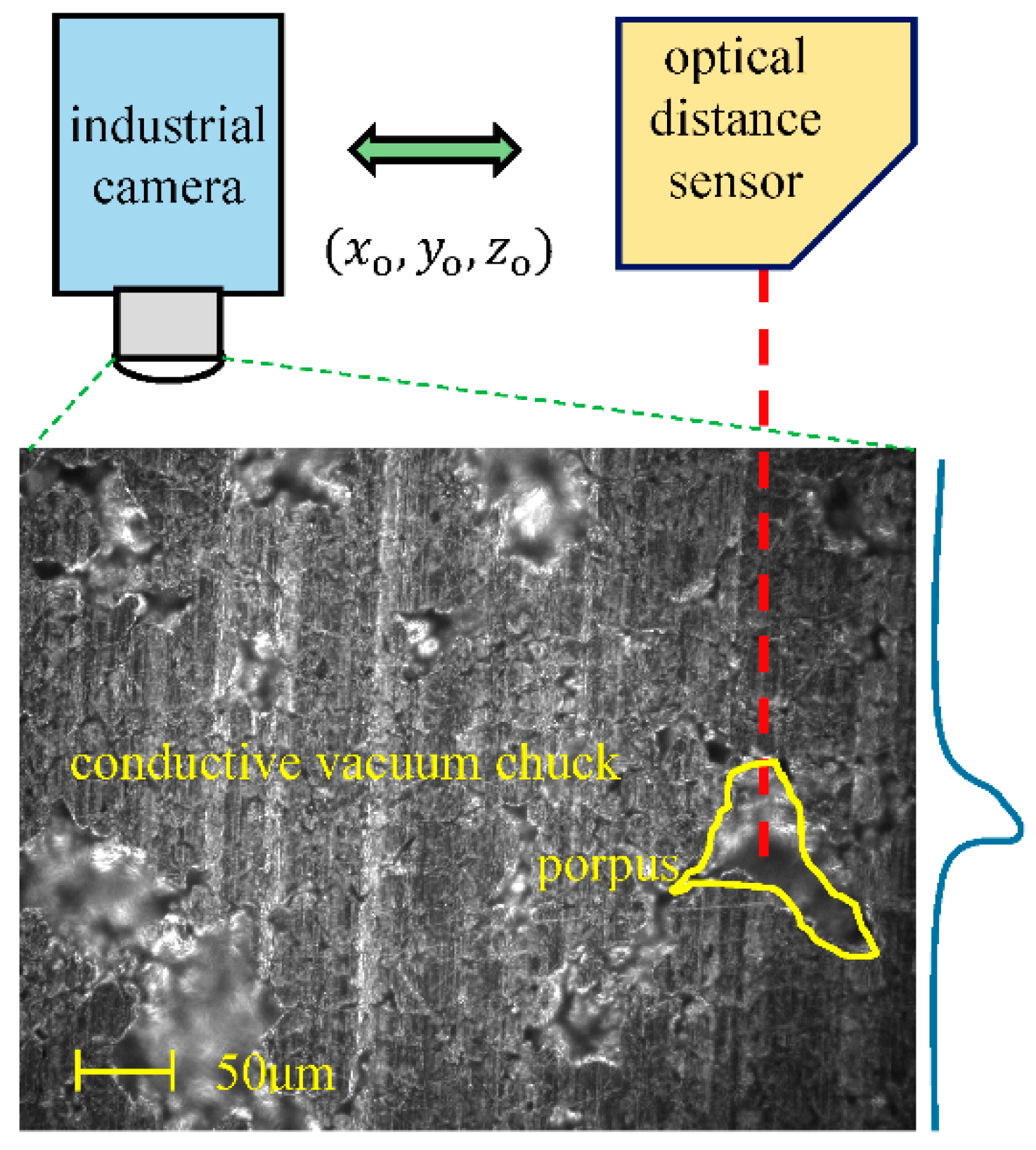
2.2. Surface Flatness of Conductive Vacuum Chuck

In PEs, non-contact and on-machine measurements are preferred; thus, an optical distance sensor (ODS) is conventionally used to measure the surface flatness in large areas [26]. It is desirable to measure the surface flatness from the upper face of the film, but this is generally not possible owing to optical discontinuities from printed patterns and film transparency. Commercial ODSs can measure these transparent films, but the refractive index of the printed patterns is usually unknown [27]. Thus, after measuring the surface flatness of the CVC, that of the film surface can be obtained based on interpolation.
The ideal position for the laser ablation, zr, must be corrected according to the surface flatness of the CVC, i.e., Δz(x,y).
z = z r + Δ z ( x , y ) ,   { ( x , y ) | x R , y R }
Figure 2 shows the relationships among the ablation head, ODS and CVC. The ODS is attached near the ablation head. The distance between the coaxial optics and ODS, Δzd, forms kinematic offsets (xo, yo, zo). Thus, the coordinates of the ODS, (x′, y′, z′), are calculated as follows:
z d ( x , y ) = z r + Δ z d ( x + x o , y + y o ) + z o = z + Δ z d ( x , y )
Measuring a surface flatness by scanning the ODS is fast and convenient. However, the ODS can cause measurement errors owing to the porosity of the CVC. The narrow spot of the ODS provides the distance from a local area; thus, a measurement error can occur owing to the porosity, as shown in Figure 2. The degree of focus of an image represents a larger area; thus, the focus position is more reliable for determining the surface flatness. The focus position is found using the AF, which scans the variations of contrast along an optical axis. The focus positions on a plane of the CVC are applicable for determining the surface flatness [28].
The AF requires a long scanning time, as the focus depth of the coaxial optics is extremely narrow. For instance, the scanning interval for the AF should be less than the focus depth; it was 10 μm in this study. Therefore, the AF should be joined with the ODS, i.e., the AF should be performed based on the ODS results. The AF determines a focal position at the optimum of contrast, σ, according to movement along the optical axis near zd [29]. The range of the movement near zd, δ, is a small value. The focus position of the AF, za, can be determined at a local maximum of the DFIs as follows:
z a ( x , y ) = max z { σ ( z ) } { z | z d δ z z d + δ ,   z R }
The contrast for the AF can be evaluated using the DFIs. The DFIs are calculated from high-frequency components and pixel-based operations, as shown in Appendix A [30]. The surface flatness using the AF can be defined according to the difference between the maximum and minimum values of za.
Δ z a ( x , y ) = z a ( x , y ) 1 2 [ max { z a ( x , y ) } + min { z a ( x , y ) } ]

2.3. Interplation of Surface Flatness of Thin Film
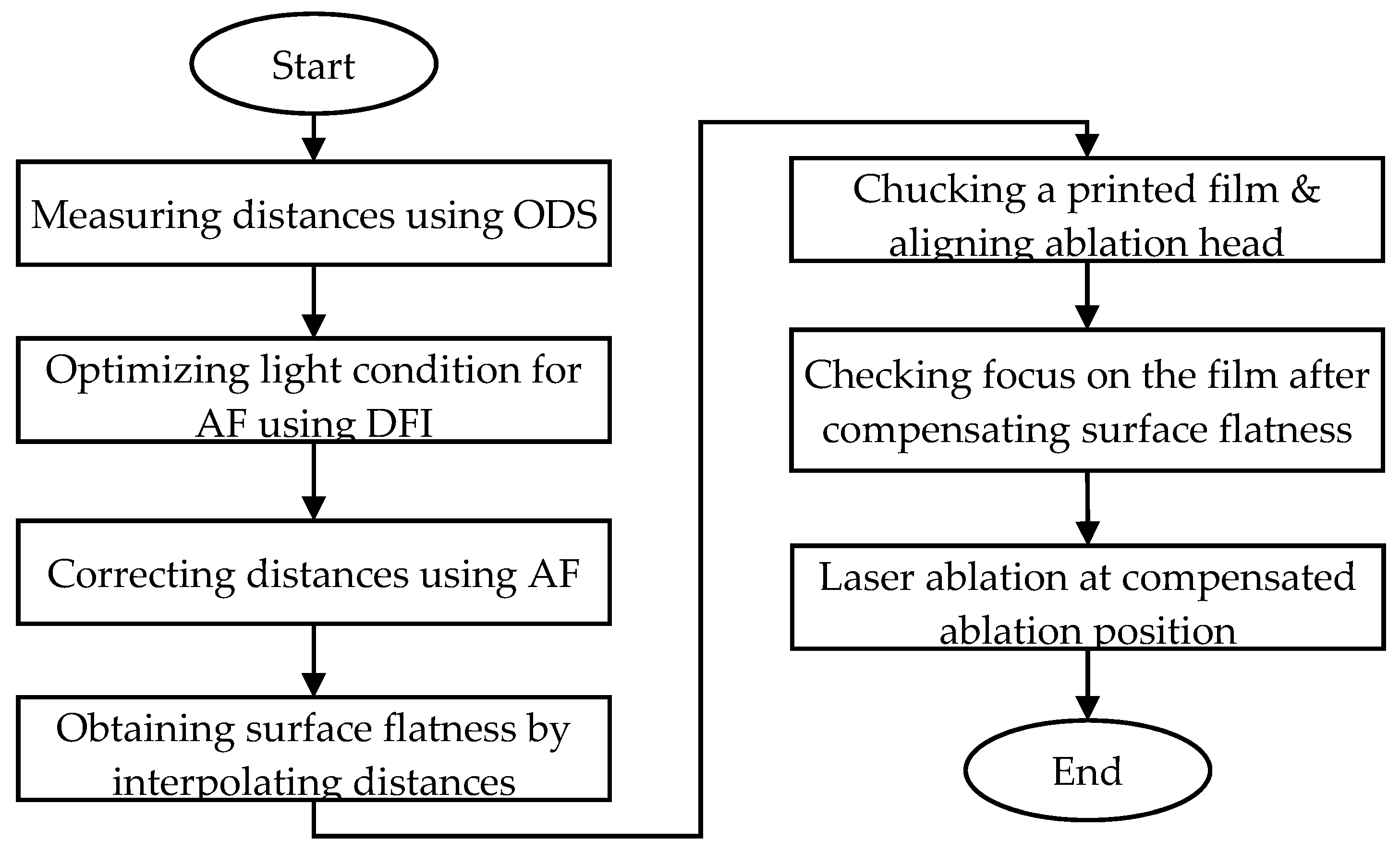
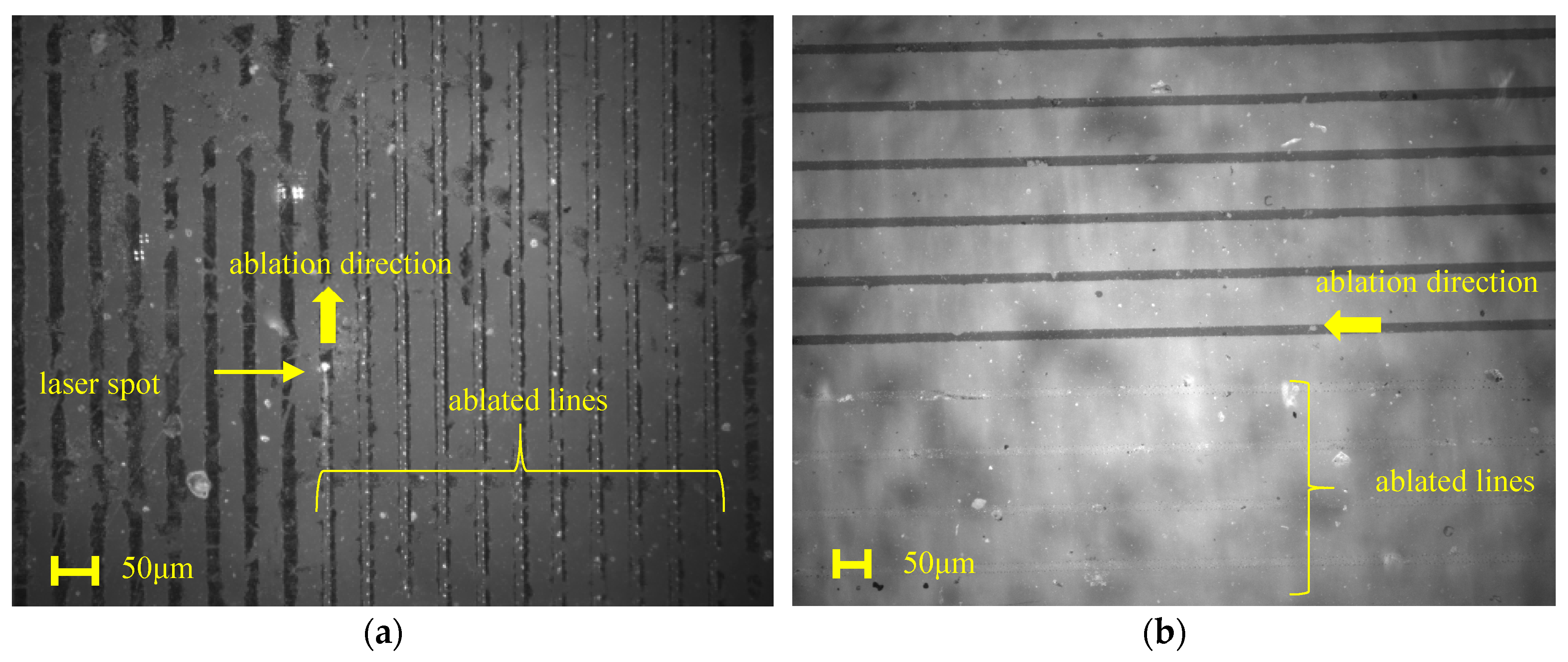
Commercial coordinate measuring machines usually obtain surface flatness values using contact methods and sampling measurement data [31]. Owing to the AF scanning time, the number of AF points in the planar directions should also be limited. The curvature of the film in the fixed state forms smoother curve than that of the CVC. Thus, the surface flatness of the film can be estimated based on a 2D interpolation of the sampling points. Bilinear interpolation is a popular interpolation approach, and normalized positions for the interpolation can be defined as follows [32]:
( u , v ) = ( x x i x i + 1 x i , y y i y j + 1 y j )
Then, the interpolated position in the planar direction by the AF can be written using the following equation [33].
z ^ a = ( 1 u ) ( 1 v ) z a ( x i , y j ) +   u ( 1 v ) z a ( x i + 1 , y j ) +   ( 1 u ) v z a ( x i , y j + 1 ) +   u v z a ( x i + 1 , y j + 1 )
Surface flatness can be also interpolated using the above concept.
Δ z ^ a = ( 1 u ) ( 1 v ) Δ z a ( x i , y j ) + u ( 1 v ) Δ z a ( x i + 1 , y j ) + ( 1 u ) v Δ z a ( x i , y j + 1 ) + u v Δ z a ( x i + 1 , y j + 1 )
Then, the interpolated position for the laser ablation on the film surface, zf, can be calculated, while considering the film thickness and air buffer from the CVC. The surface flatness is used for ablation and inspection just by adding constant values in practice.
z f ( x , y ) = z ^ a ( x , y ) + h = Δ z ^ a + c

3. Experiment

3.1. Laser Ablation System

The laser ablation system is composed of a linear stage, ablation head, high-power laser source, light source, CVC, controller and ODS. The linear stage transfers the ablation head above the CVC based on Cartesian coordinates. In this study, the xy axes comprised the gantry structure, and were driven using high-speed linear motors. The z-axis was constructed using a high-accuracy ball screw and was installed on the gantry. The ablation head was attached on the z-axis, and the ODS was equipped near the ablation head, as shown in Figure 3a.
The light source supplied variable color light to the ablation sample, so as to monitor the micro-patterns using the industrial camera. For optimization of the light color and intensity, the original light colors of RGBW LEDs were used. The initial intensity of a selected color for the AF was set to 30% of the maximum light power. Then, the focus was scanned on the CVC by moving the focal axis and was determined at the maximum of the DFIs. The light intensity was also determined at the maximum of the DFIs by adjusting the light power in the focus position. The optimal light color and intensity values for the AF were also achieved using the maximum values of the DFIs. After the focus of the industrial camera was determined under RGBW colors, the light color and intensity were also determined for the AF at the maximum of the DFIs.
The ablation sample was produced through the R2R process, i.e., printing micro-patterns on a transparent and thin film. The patterns (shown in Figure 3b) consisted of micro-lines ranging from 10 μm to 50 μm, and were printed using silver nanoparticle ink. The film was polyethylene terephthalate (PET) with a thickness of 100 μm. The ablation sample was fastened to the CVC using a vacuum. The optimal color light reflected on the ablation sample passed the object lens and half-mirror. The industrial camera acquired images for inspecting the patterns and aligning the ablation direction. Then, a laser beam from the high-power laser source was injected into the side port of the ablation head, reflected on the half-mirror into a right angle, and focused on the ablation sample through an object lens. The laser beam blasted a defective pattern on the film, and the laser ablation was observed using the industrial camera.
The operating software for laser ablation was constructed using Visual Studio and OpenCV. The software maneuvered the stage, industrial camera, color light source, high-power laser, and ODS. The source code for the DFIs was implemented into a dynamic-link library based on OpenCV. The procedure of experiment is shown in Figure 4, and the specifications of the ablation head are summarized in Table 1.

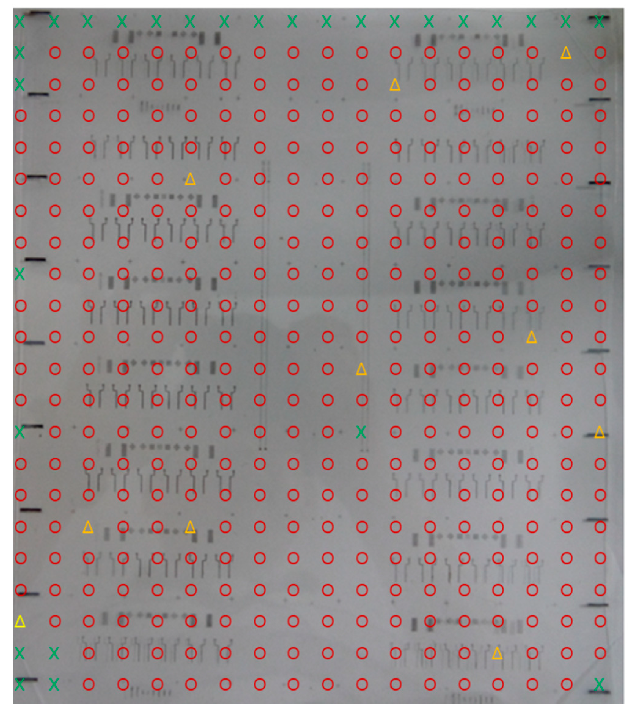
3.2. Interpolation and Surface Flatness

The AF points in the planar directions, (xi, yj), were determined by dividing the CVC surface into a rectangular grid. The values of zd(xi + x0, yj + y0) were measured using the ODS, and then, AF was performed to correct zd under the optimum light color and intensity values. za(xi, yj) was obtained from the corrected value, and a contour map of the surface flatness was constructed by bilinear interpolation. Signals of thickness measurement mode in the ODS were used to verify the interpolation. After entire area of the CVC was covered with a clean film, a vacuum was applied to fix the film. Then, the ODS was tilted and sensor parameters were varied to switch into the thickness measurement mode. Signals of the reflection from the upper surface were used to obtain surface flatness.
After the ablation sample was mounted on the CVC, and the patterns on the sample were inspected at the interpolated position, zf(xi + α, yj + β), to verify the proposed method. The distinctness of the images acquired at the interpolated position was examined to determine the usability for laser ablation. Laser ablation was performed to remove line patterns on the ablation sample.

4. Results and Discussion

The optimum light conditions for the AF were determined at the maximum of the DFIs. Figure 5 shows that the curves of the DFIs usually form a single peak during focusing and lighting. Many DFIs showed maxima at the same focal position, although some DFIs presented different foci or had diverged. After determining the focus position, the light intensity was determined at the maximum values of the DFIs by increasing the light power. These focusing and lighting procedures were repeated for the other original colors. Figure 5a shows the variations of the DFIs according to the intensity of blue light. A threshold pixel became saturated, and a derivative-based correlation showed different focus positions; thus, these DFIs were excluded from determining the light conditions. The energy Laplacian and Tenenbaum gradient showed larger variations than that for the other DFIs. However, the energy Laplacian showed noise patterns and coarse curvature in the graph; the Tenenbaum gradient was finally selected for the AF. Figure 5b shows the responses of the Tenenbaum gradient according to the original color lights. From comparing the color responses of the Tenenbaum gradient, the highest maximum was formed when using the red color; thus, red light was selected for the AF. In addition, the color of the high-power laser was green (532 nm), i.e., a complementary color of the AF color; thus, the determined light color was advantageous for monitoring the laser ablation.
The variation in the grid density of the AF points and surface flatness values when using the ODS is shown as contour maps in Figure 6. A longer distance implies a farther distance from the CVC surface, and is lower on the CVS surface. Thus, the color in the contour maps changes from blue to red according to the −Δzd value. The red area indicates a local high surface with a long distance from the ODS, and the blue area indicates the inversion. The values of the indicators on the right of the contour maps show the minimum and maximum values of −Δzd. The contour maps show that the top-left of the CVC has lower values and the bottom-left has higher values. Additionally, the contour maps show that the top-right has slightly higher values and the bottom-right represents the average. The overall tendency of the contour maps in Figure 6 is similar to the variation of the grid density. However, the contour maps became coarse as the grid density increased. The contour map at a low grid density was smooth, but discontinuities such as dots and speckles increased at high grid density. The blue dots in the 50 × 50 map were caused by local cracks and porosity on the CVC. This indicates that a large number of sampling positions does not guarantee high-accuracy of surface flatness values. As shown in Figure 2, the concave curvature of the porosity is very small whereas the curvature of the CVC is very large. Thus, the blue dots should be excluded when approximating the surface flatness and positions of the ODS. The curvature of a thin film fixed on the CVC will have a smooth surface; thus, the effect of these local flaws on the surface flatness of the film decreases. In the contour maps, an 8 × 8 grid density was considered optimal when considering the smoothness, local variations, and focusing time.
Figure 7a shows contour maps of the surface flatness after the AF and −Δza according to the grid density. The overall tendencies of the contour maps were similar as shown in Figure 6, but the maps varied locally as the grid density increased. The difference between the contour maps from the ODS and AF was small at a lower grid density, but the difference became distinct at higher grid densities. Figure 7b shows a contour map of the surface flatness using the thickness measurement mode on a clean film. Overall shapes of Figure 7a,b are similar and some local discontinuities were removed compared with Figure 6. The error between the reflection method and our interpolation was ±3.0 μm but the error between the reflection method and the CVC was ±4.5 μm.
After mounting a transparent and thin film fabricated using the R2R, images were acquired at the interpolated position for the laser ablation, zf. The (x, y) points of the interpolated positions were achieved by slicing the contour maps of the 8 × 8 grid (shown in Figure 6) into a 24 × 24 grid. Then, the focus quality was investigated at the interpolated position. In the 24 × 24 grid of the CVC, 18 × 20 points were placed on the ablation sample. Figure 8 shows the sample images acquired at the interpolated positions. Three images showed focused patterns; another (at the bottom-right) was slightly defocused.
The distribution of the focus quality is mapped in Figure 9. O denotes focused, Δ denotes slightly defocused but ablatable, and X denotes completely defocused. The corresponding counts of points were 322, 10, and 28. Thus, 92.2% of the points in the ablation sample were available for laser ablation. However, 96.4% of the defocused points were placed at the edges of the ablation sample, and one point was located inside. This indicates that the chucking force using the vacuum is weak at the edges owing to leak; hence, the edge area floats relative to the inside and margin at the edge area is required when designing PE patterns. The defocused point inside was caused by large scratches on the CVC, which formed wrinkles in the film. These facts imply that scratches and bruises must be removed constructing the CVC for laser ablation of PEs.
Figure 10 shows the laser ablation on the line patterns on the compensated position using alignment and surface flatness. Automatic alignment found positional deviation on XYθ directions and the deviation was applied to XY ablation position. Positions for laser ablation calculated using end edge of a pattern group, line pitch and line length. Z ablation positions were compensated using surface flatness according to XY machine coordinates. The left image shows that the ablation laser was focused with a 5 μm spot diameter and removed 10 μm-width line patterns on vertical direction. The right image shows laser ablation cleared line-patterns on horizontal direction using 7 μm spot diameter. Figure 10 shows that the micro lines printed on PET was removed after laser ablation.
The results show that these surface flatness values should be applied to calibrate laser ablation systems for large-area processes and that their compensation should be an essential function of manufacturing systems for PEs. Laser ablation is useful for recovering faulty devices; thus, it is advantageous to increase the production yield. Measurement time of a laser interferometer is shorter and measurement accuracy is higher than those of the proposed method. However, the laser interferometer requires installation time and coordinate transformation which cause kinematic errors. The proposed measurement uses on-machine devices under a single coordinate, thus additional installation and coordinate transform are not required. Automatic measurement process provides operational convenience and efficient working time.
On the other hand, the ablation head was used for simple monitoring in this study, but various functions can be achieved using artificial intelligence (AI) in the future. AI is currently introduced in recent researches of laser ablation [34] and the laser ablation system in this study is advantageous for data mining. The ablation head can collect image-based data which can be linked with the mechanical data of high accuracy. These high-quality data will be appropriate for training AI functions, such as kinematic alignment, light optimization, determination of ablation quality as well as acquisition of surface flatness.

5. Conclusions

In this study, a method for measuring the surface flatness of a transparent and thin film was proposed, based on the AF for the laser ablation of PEs. The defocusing of laser ablation owing to the chucking bending of the flexible and thin film can be reduced by the surface flatness. The surface flatness of the film was estimated from that of the CVC based on a non-contact and optical method considering the transparency, thinness, and printed patterns of the film. The surface flatness of the CVC was measured using an optical distance sensor according to the variable grid density. The proper grid density of the measurement points was determined by considering the porosity of the CVC and coarseness of the contour maps. AF was performed to correct the measured position by the ODS, as the errors caused by the ODS were caused by localities. An interpolated position was obtained from the surface flatness as corrected by the AF. The results showed that 92.2% of the test points were usable for laser ablation and most of defocus was caused by the vacuum leak at the edge. The proposed method is available in the normal areas of laser ablation and makes it possible to provide large-area ablation; thus, it should be an indispensable function in a laser ablation system for PEs. The automatic on-machine measurement provides operational convenience and efficient working time without additional device installation. The proposed method also contributes to the repair of defective devices, thus improving the production yield of PEs.

Author Contributions

Conceptualization, J.Y.H. and H.K. (Heuiseok Kang); methodology, Y.J.M. and H.K. (Heuiseok Kang); software, H.K. (HyungTae Kim); validation, Y.J.M. and J.Y.H.; formal analysis, Y.J.M.; investigation, H.K. (Heuiseok Kang); resources, H.K. (Heuiseok Kang); data curation, Y.J.M.; writing—original draft preparation, H.K. (HyungTae Kim); writing—review and editing, H.K. (HyungTae Kim); visualization, H.K. (HyungTae Kim); supervision, J.Y.H.; project administration, J.Y.H.; funding acquisition, J.Y.H. All authors have read and agreed to the published version of the manuscript.

Funding

This study has been conducted with the support of the Korea Institute of Industrial Technology as “Development of root technology for multi-product flexible production (KITECH EO-20-0015).

Conflicts of Interest

The authors declare no conflict of interest.

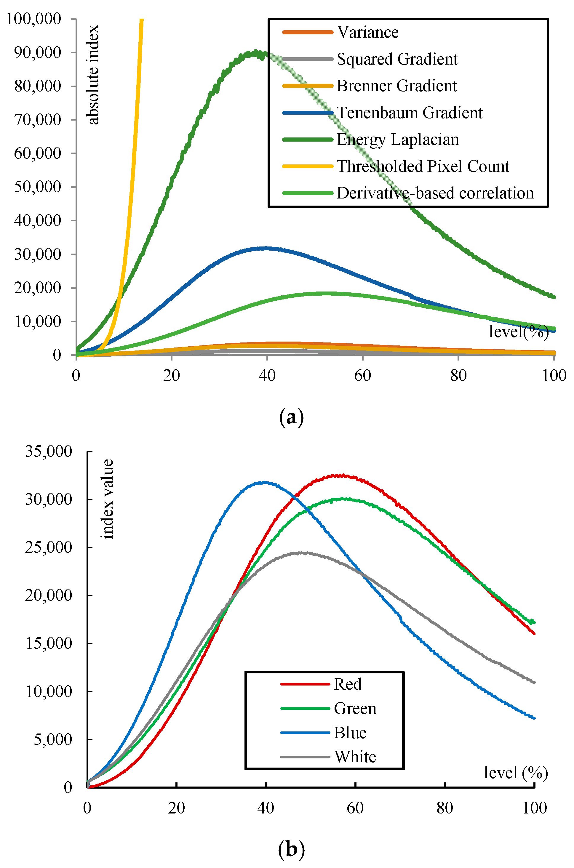
Appendix A. Digital Focus Indices

DFIFormulationColor
Brightness σ br = 1 m n i m j n I ( i , j ) -
Contrast σ ct = I max I min I max + I min -
Variance σ vr = 1 m n i m j n [ I ( i , j ) σ br ] 2 brown
Squared Gradient (Δ = 1) σ sq = 1 ( m 1 ) ( n 1 ) i m j n [ { Δ i I ( i , j ) } 2 + { Δ j I ( i , j ) } 2 ] grey
Brenner gradient (Δ = 2) σ Br = 1 ( m 2 ) ( n 2 ) i m j n [ { Δ i I ( i , j ) } 2 + { Δ j I ( i , j ) } 2 ] goldenrod
Tenenbaum gradient σ Tn = 1 ( m 2 ) ( n 2 ) i m j n [ { S i ( i , j ) } 2 + { S j ( i , j ) } 2 ] blue
Energy Laplacian σ en = 1 ( m 1 ) ( n 1 ) i m j n [ L * I ( i , j ) ] 2 dark green
Histogram Entropy σ hi = i m p k l o g 2 p k -
Thresholded Pixel Count σ tp = i m j n s ( I ( i , j ) , θ )       s ( x , θ ) = { 1 x θ 0 x > θ yellow
Normalized Variance σ nv = σ var σ bright -
Derivative-based Correlation σ dc = 1 ( m 1 ) ( n 1 ) i m j n [ I ( i + 1 , j + 1 ) I ( i , j ) σ br 2 ] lime
Auto-correlation σ ac = 1 ( m 1 ) ( n 1 ) i m j n [ I ( i + 1 , j + 1 ) I ( i , j ) I 2 ( i , j ) ] -

References

  1. Venkata Krishna, R.R.; Venkata Abhinav, K.; Kathik, P.S.; Surya Prakash, S. Conductive silver inks and their applications in printed and flexible electronics. RSC Adv. 2015, 2015, 77760–77790. [Google Scholar]
  2. Phillips, C.O.; Beynon, D.G.; Hamblyn, S.M.; Davies, G.R.; Gethin, D.T.; Claypole, T.C. A Study of the Abrasion of Squeegees Used in Screen Printing and Its Effect on Performance with Application in Printed Electronics. Coatings 2014, 4, 356–379. [Google Scholar] [CrossRef] [Green Version]
  3. Kang, D.; Kim, J.; Kim, I.; Choi, K.H.; Lee, T.M. Experimental Qualification of the Process of Electrostatic Spray Deposition. Coatings 2019, 9, 294. [Google Scholar] [CrossRef] [Green Version]
  4. Park, J.P.; Shin, K.; Lee, C. Roll-to-Roll Coating Technology and Its Applications: A Review. Int. J. Precis. Eng. Manuf. 2016, 17, 537–550. [Google Scholar] [CrossRef]
  5. Chen, S.; Chen, W.; Liu, J.; Chen, W. A roller posture adjustment device with remote-center-of-motion for roll-to-roll printed electronics. Precis. Eng. 2019, 56, 172–183. [Google Scholar] [CrossRef]
  6. Lu, B.H.; Lan, H.B.; Liu, H.Z. Additive manufacturing frontier: 3D printing electronics. Opto-Electron. Adv. 2018, 1, 170004. [Google Scholar] [CrossRef]
  7. Yu, J.H.; Kang, K.T.; Hwang, J.Y.; Lee, S.H.; Kang, H. Rapid Sintering of Copper Nano Ink Using a Laser in Air. Int. J. Precis. Eng. Manuf. 2014, 15, 1051–1054. [Google Scholar] [CrossRef]
  8. Kim, S.H.; Kang, H.; Kang, K.; Lee, S.H.; Cho, K.H.; Hwang, J.Y. Effect of Meniscus Damping Ratio on Drop-on-Demand Electrohydrodynamic Jetting. App. Sci. 2018, 8, 164. [Google Scholar] [CrossRef] [Green Version]
  9. Ram, O. Performance optimization of electronic circuits laser repair. In Proceedings of the SPIE LAMOM XIX, San Francisco, CA, USA, 1–6 February 2014; Volume 8967, p. 89671H. [Google Scholar]
  10. Seiler, A.L.; Chartier, I.; Laurent, J.Y.; Suhonen, R.; Hast, J.; Känsäkoski, M.; Petkov, P.; Blaudeck, T.; Baumann, R.R. Eximer laser ablation as industrial production tool for structuring ITO anodes for flexible OLEDs. In Proceedings of the LOPEC Conference, Frankfurt, Germany, 31 May–2 June 2010; pp. 1–4. [Google Scholar]
  11. Lee, K.; Ki, H. Fabrication and optimization of transparent conductive films using laser annealing and picosecond laser patterning. App. Surf. Sci. 2017, 420, 886–895. [Google Scholar] [CrossRef]
  12. IEC 62899-201 Edition 1.1 Printed Electronics—Part 201: Materials—Substrates. Available online: https://webstore.iec.ch/publication/64210 (accessed on 4 August 2020).
  13. Seong, J.; Kim, S.; Park, J.; Lee, D.; Shin, K.H. Online noncontact thickness measurement of printed conductive silver patterns in Roll-to-Roll gravure printing. Int. J. Precis. Eng. Manuf. 2015, 16, 2265–2270. [Google Scholar] [CrossRef]
  14. Choi, Y.M.; Yoo, H.; Kang, D. Large-area thickness measurement of transparent multi-layer films based on laser confocal reflection sensor. Measurement 2020, 153, 107390. [Google Scholar] [CrossRef]
  15. Bornemann, N.; Dörsam, E. A flatbed scanner for large-area thickness determination of ultra-thin layers in printed electronics. Opt. Exp. 2013, 21, 21897–21911. [Google Scholar] [CrossRef] [PubMed]
  16. Lee, C.; Kang, H.; Kim, H.; Nguyen, H.A.D.; Shin, K. Quality control with matching technology in roll to roll printed electronics. J. Mech. Sci. Technol. 2010, 24, 315–318. [Google Scholar] [CrossRef]
  17. Abbel, R.; Galagan, Y.; Groen, P. Roll-to-Roll Fabrication of Solution Processed Electronics. Adv. Eng. Mater. 2018, 20, 1701190. [Google Scholar] [CrossRef] [Green Version]
  18. Zou, X.; Zhao, X.; Li, G.; Li, Z.; Sun, T. Non-contact on-machine measurement using a chromatic confocal probe for an ultra-precision turning machine. Int. J. Adv. Manuf. Technol. 2017, 90, 2163–2172. [Google Scholar] [CrossRef]
  19. Xu, C.; Chen, L.; Yin, J. Method for absolute flatness measurement of optical surface. App. Opt. 2009, 48, 2536–2541. [Google Scholar] [CrossRef]
  20. Une, A.; Yoshitomi, K.; Mochida, M. Dynamic deformation of a wafer above a lift hole and influence on flatness due to chucking. Microelectron. Eng. 2011, 88, 2163–2166. [Google Scholar] [CrossRef]
  21. Mikkelson, A.; Engelstad, R.; Sohn, J.; Lovell, E. Effect of electrostatic chucking and film thickness uniformity on extreme ultraviolet lithography mask flatness. J. Vac. Sci. Technol. B 2004, 22, 3043. [Google Scholar] [CrossRef]
  22. Mane, V.V. An Effective Method to Reduce Smearing in Machining of Metallic Foams. Master’s Thesis, Iowa State University, Ames, IA, USA, 2016. [Google Scholar]
  23. Banhart, J. Manufacture, characterisation and application of cellular metals and metal foams. Prog. Mater. Sci. 2001, 46, 559–632. [Google Scholar] [CrossRef]
  24. Lee, C.C.; Huang, P.C.; Wang, K.S. Flexural Capability of Patterned Transparent Conductive Substrate by Performing Electrical Measurements and Stress Simulations. Materials 2016, 9, 850. [Google Scholar] [CrossRef] [Green Version]
  25. Kuwahara, K.; Taguchi, R.; Masayuki, K.; Akamatsu, N.; Tokumitsu, K.; Shishido, A. Experimental and theoretical analyses of curvature and surface strain in bent polymer films. Appl. Phys. Express 2020, 13, 056502. [Google Scholar] [CrossRef] [Green Version]
  26. Li, X.; Fan, B.; Jiang, H.; Zhao, H. Non-contact large-scale separated surfaces flatness measurement by using laser beam and laser distance sensor. In Proceedings of the SPIE icOPEN, Singapore, 14–16 April 2015; Volume 9524, p. 95241N. [Google Scholar]
  27. Hilfiker, J.N.; Stadermann, M.; Sun, J.; Tiwald, T.; Hale, J.S.; Miller, P.E.; Aracne-Ruddle, C. Determining thickness and refractive index from free-standing ultra-thin polymer films with spectroscopic ellipsometry. App. Surf. Sci. 2017, 421(Pt. B), 508–512. [Google Scholar] [CrossRef]
  28. Giusca, C.L.; Claverly, J.D.; Sun, W.; Leach, R.K.; Helmli, F.; Chavigner, M.P.J. Practical estimation of measurement noise and flatness deviation on focus variation microscopes. CIRP Ann. 2014, 63, 545–548. [Google Scholar] [CrossRef]
  29. Kim, H.T.; Cho, K.Y.; Kim, J.; Jin, K.C.; Kim, S.T. Robust Parameter Design of Derivative Optimization Methods for Image Acquisition Using a Color Mixer. J. Imaging 2017, 3, 31. [Google Scholar] [CrossRef]
  30. Yao, Y.; Abidi, B.; Doggaz, N.; Abidi, M. Evaluation of Sharpness Measures and Search Algorithms for the Auto-Focusing of High Magnification Images. In Proceedings of the SPIE Visual Information Processing XV, Orlando, FL, USA, 17–21 April 2006; Volume 6246, p. 6246G. [Google Scholar]
  31. Raghynanda, R.; Venkateswara Rao, P. Selection of sampling points for accurate evaluation of flatness error using coordinate measuring machine. J. Mater. Process. Technol. 2008, 202, 240–245. [Google Scholar] [CrossRef]
  32. Press, W.H.; Teukolsky, S.A.; Vetterling, W.T.; Flannery, B.P. Numerical Recipes in C—The Art of Scientific Computing, 2nd ed.; Cambridge University Press: Cambridge, UK, 1992; pp. 123–124. [Google Scholar]
  33. Chen, H.C.; Wang, W.J. Fuzzy-adapted linear interpolation algorithm for image zooming. Signal. Process. 2009, 89, 2490–2502. [Google Scholar] [CrossRef]
  34. Chen, L.W.; Yin, Y.M.; Li, Y.; Hong, M.H. Multifunctional inverse sensing by spatial distribution characterization of scattering photons. Opto-Electron. Adv. 2019, 2, 190019. [Google Scholar] [CrossRef] [Green Version]
Figure 1. Conceptual diagram of a laser ablation optics.
Coatings 10 00885 g001
Figure 2. Measuring surface flatness of a conductive vacuum chuck (CVC) with high porosity.
Coatings 10 00885 g002
Figure 3. (a) Laser ablation head and optical distance sensor (ODS) (b) pattern drawing for micro-printing on a transparent and thin film.
Coatings 10 00885 g003
Figure 4. Procedure to obtain surface flatness and performs laser ablation in experiment.
Coatings 10 00885 g004
Figure 5. Variations of (a) digital focus indices (DFIs) under blue light (b) Tenenbaum gradient under RGBW light according to light intensity.
Coatings 10 00885 g005
Figure 6. Variation of grid density and interpolation of surface flatness using an optical distance sensor.
Coatings 10 00885 g006
Figure 7. Variations of grid density and interpolation of surface flatness using (a) AF and (b) thickness measurement.
Coatings 10 00885 g007
Figure 8. Line-pattern images acquired on compensated position using surface flatness and printed with (a) 25 μm pitch (b) 100 μm (c) an incline and (d) 50 μm.
Coatings 10 00885 g008
Figure 9. Focus map on an entire film after applying surface flatness (O = in-focus, Δ = ablatable, X = out-of-focus).
Coatings 10 00885 g009
Figure 10. Images of ablation tests using surface flatness in (a) horizontal and (b) vertical directions.
Coatings 10 00885 g010
Table 1. Specification of a repair system.
ComponentsContentsValues
Linear stageaxis
stroke (x/y/z)
speed (x/y/z)
accuracy (x/y/z)
vacuum chuck size
3 (dual x, y, z)
450/400/100 mm
500/500/100 mm
±2/±2/±2 μm
200 mm × 200 mm
Ablation headimage size
frame rate
FOV
focus depth
ablation depth
mount
camera interface
light source
1624 × 1236 pixels
50 frames/s
0.8 mm × 0.6 mm
10 μm
30 μm
C-mount
GigE
RGBW mixing
Optical distance sensormeasuring range
resolution
measuring rate
light source
interface
0–10 mm
0.15 μm
20 kHz
650 nm laser diode
Ethernet

