Article

Comparison of Carbon Thin Films with Low Secondary Electron Yield Deposited in Neon and Argon

National Synchrotron Radiation Laboratory, University of Science and Technology of China, Hefei 230029, China
*
Authors to whom correspondence should be addressed.
Coatings 2020, 10(9), 884; https://doi.org/10.3390/coatings10090884
Submission received: 3 August 2020 / Revised: 9 September 2020 / Accepted: 10 September 2020 / Published: 14 September 2020

Abstract

:
Modification of vacuum chamber surface properties by introducing a layer of material with low secondary electron yield (SEY) is one of the most useful solutions to suppress the electron-cloud in high-energy particle accelerators. In the present work, amorphous carbon thin films have been produced by DC magnetron sputtering with Neon and Argon sputtering gases. Microstructures of the thin films have been characterized by using scanning electron microscopy (SEM) and atomic force microscopy (AFM). The sp2 and sp3 hybridized carbon atoms are evaluated using X-ray photoelectron spectroscopy (XPS) and Raman spectroscopy. The amorphous carbon coatings comprise tiny granularities of tens of nanometers. The amorphous carbon films show more graphite-like properties as revealed by XPS and Raman spectroscopy. The secondary electron emission measurement results indicate that amorphous carbon coatings present SEY of <1.2. The thin film deposited by Ne exhibits a higher sp2 hybridization content, leading to a slightly lower SEY compared with the film produced with Ar.

1. Introduction

The vacuum chamber of high-energy particle accelerators contains small amounts of residual gas, ions, low-energy electrons. Synchrotron radiation from the particle beam generates electrons by photoemission from the wall of the beam pipe or through ionisation of the residual gas by beam-gas interactions. The charged particle beam then accelerates the initial electrons resulting that these initial electrons hit the wall of the chamber and produce secondary electrons, which in turn can be accelerated by the following bunch. If the secondary electron yield of the vacuum chamber is larger than unity, then electron multipacting may occur [1]. A large density of electrons can build up inside the beam chamber, leading to the formation of an electron cloud.
Electron cloud build-up can significantly affect the quality of the beam and machine operation such as LHC, KEKB, RHIC, PEP=II and so forth [2]. Adverse effects from electron cloud that have been observed in recent years include dynamic pressure rise, transverse emittance blow-up, thermal load in cryogenic vacuum systems as well as beam lose [3,4,5]. In radio frequency (RF) cavities, electron multipacting can also absorb RF power and lead to power loss. Additionally, the electrons can desorb gas from the walls increasing the pressure in the beam pipe or RF cavities [6]. Therefore, electron cloud is a main limitation for the achievement of high-quality beam in high-energy modern accelerators.
Electron cloud mitigation is the emphasis of research over more than 50 years, many methods, like surface conditioning, thin film coating, electrodes clearing and grooved chamber and so forth, have been proposed to suppress the electron cloud [7,8,9,10]. One of the most effective methods is to coat vacuum chambers with materials of intrinsically low secondary electron yield (SEY), because secondary electron emission plays a significant role in the build-up of electron cloud. The well-known Ti-Zr-V film that requires thermal activation at temperatures higher than 180 °C is infeasible for some vacuum pipes of modern accelerators where cryogenic temperature condition is a prerequisite. In this regards, thin films with low initial SEY, which does not require in-situ bake-out, should be developed. For such a purpose, amorphous carbon (a-C) coating have been investigated in recent years [11,12,13] and evaluated at cryogenic temperature for the High Luminosity LHC (HL-LHC) project [14].
Carbon material is known to have a low SEY in its graphite allotropic form mainly ascribing to the sp2 hybrids in graphite. [15,16,17]. The well-developed DC magnetron sputtering has been widely employed to fabricate carbon-based thin films because of its compatibility to the complex geometry of the accelerator components to be coated. On the other hand, carbon thin films can be deposited easily on large areas and obtain high structural quality using DC magnetron sputtering method. Different discharge gases and different deposition parameters (such as discharge gas pressure, working power, substrate temperature) have been applied and imposes great influences on the quality and properties of the thin films [18,19,20].
In this work, amorphous carbon thin films have been deposited and investigated as one of the solutions to mitigate electron-cloud for Super Proton-Proton Collider (SPPC). Amorphous carbon thin films are deposited with a DC magnetron sputtering apparatus using graphite targets and different discharge gases. The a-C thin films have been characterized by scanning electron microscopy (SEM) to observe the surface morphology. The atomic force microscopy (AFM) was used to study the microstructure of the surface and to estimate its average roughness (Ra). The sp2 and sp3 contents of the thin film was compared and distinguished by X-ray photoelectron spectroscopy (XPS) and Raman spectrum. Finally, the SEY measurement was employed to measure the secondary electron emission characteristic of the thin films. The contribution of various sputtering gases on the film was investigated as well.

2. Apparatus and Methods

2.1. Sample Preparation

The amorphous carbon coatings were deposited onto the polished silicon wafer by a DC magnetron sputtering system. The deposition apparatus mainly consisted of StSt pipe, vacuum gauge, solenoid, cathode, gas flow control system, power supply, turbo molecular pump unit. A graphite rod of Φ 20 mm × 500 mm was placed in the center of the pipe to serve as the cathode. A magnetic field of 150 Gauss was provided by a solenoid. The sputtering parameters are presented in Table 1.
Polished silicon wafer substrates were mounted inside the chamber. Before deposition, the silicon wafers were ultrasonically cleaned using acetone and ethyl alcohol. Then they were washed by deionized water and dried in nitrogen atmosphere. The deposition was conducted without external heating. The surface temperature of vacuum pipe during coating was 200 °C ascribed to the discharge power. In this work, various discharge gases, both neon and argon, were used to study their influences on surface characteristics and SEY.

2.2. SEY Measurement

The SEY measurement system consisted of an ultra-high vacuum chamber equipped with a Kimball Physics electron gun (EGL-2022, Kimball Physics, Wilton, NH, USA). The electron gun can provide primary electrons (PE) of 50–5000 eV targeting directly to the surface of the samples. The electron gun worked in Emission Current Control (ECC) mode to ensure its stability. During the SEY test, the vacuum pressure was 1 × 10⁻⁹–2 × 10⁻⁹ mbar and the room temperature was 298 K.
The schematic diagram of the SEY test is shown in Figure 1. The Faraday cup was biased to +70 V in order to collect all secondary electrons emitted from the sample, whereas the sample was biased to −5 V to avoid arresting secondary electrons. The electron dose during the test was 1 × 10⁻⁸ C·mm−2. The samples had a dimension of 10 mm × 10 mm × 0.5 mm. The precision of the SEY values was evaluated to be 2.6%.
The SEY (δ) denotes the ratio of emitted secondary electrons (SEs) to primary electrons (PEs) incident to the surface. It is defined as the ratio of the number of secondary electrons, ISEY, to the number of incident electrons, IP and is calculated as Equation (1):
δ   =   I SEY I P   =   I F I F   +   I S ,
where IF is Faraday cup-to-ground current, IS is sample-to-ground current. Both of them are measured by a Keithley 2400 picoammeter. The most important value for a SEY curve is the maximum SEY, called δmax and the corresponding primary electron energy, called Emax.

2.3. Characterization Method

The microstructures of the amorphous carbon films were studied by a Sirion 200 (FEI, Hillsboro, OR, USA) Schottky field scanning electron microscope (SEM). Atomic force microscope (AFM) measurements were performed through a DI Innova (Veeco, NY, USA) scanning probe microscope, in order to observe the surface morphology of the samples.
In addition, surface chemical composition was evaluated by using X-ray photoelectron spectroscopy (XPS). The measurements were performed with a Thermo ESCALAB 250Xi (Thermo Scientific, Waltham, MA, USA) using a monochromatic Al Kα X-ray source (hν = 1486.6 eV) with a beam spot size of 500 μm at 150 W. The instrument also includes a hemispherical analyzer at 45 degrees towards the sample. In this work, all Raman data were tested by a LabRam-HR (JY, France) Raman microscope system with an Ar ion laser at λ = 514 nm. Five spots distributed evenly on each sample were measured. The Raman spectra data were best-fitted by using Gaussian and Lorentzian functions.

3. Results

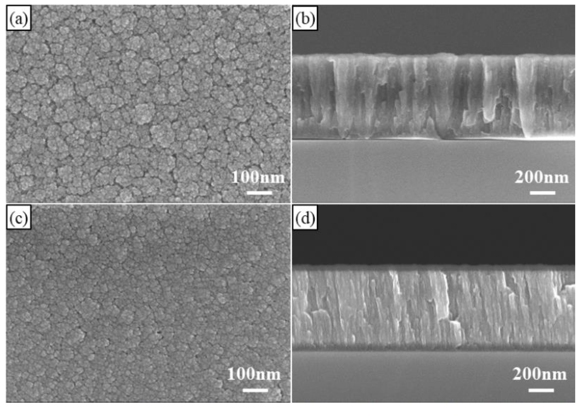
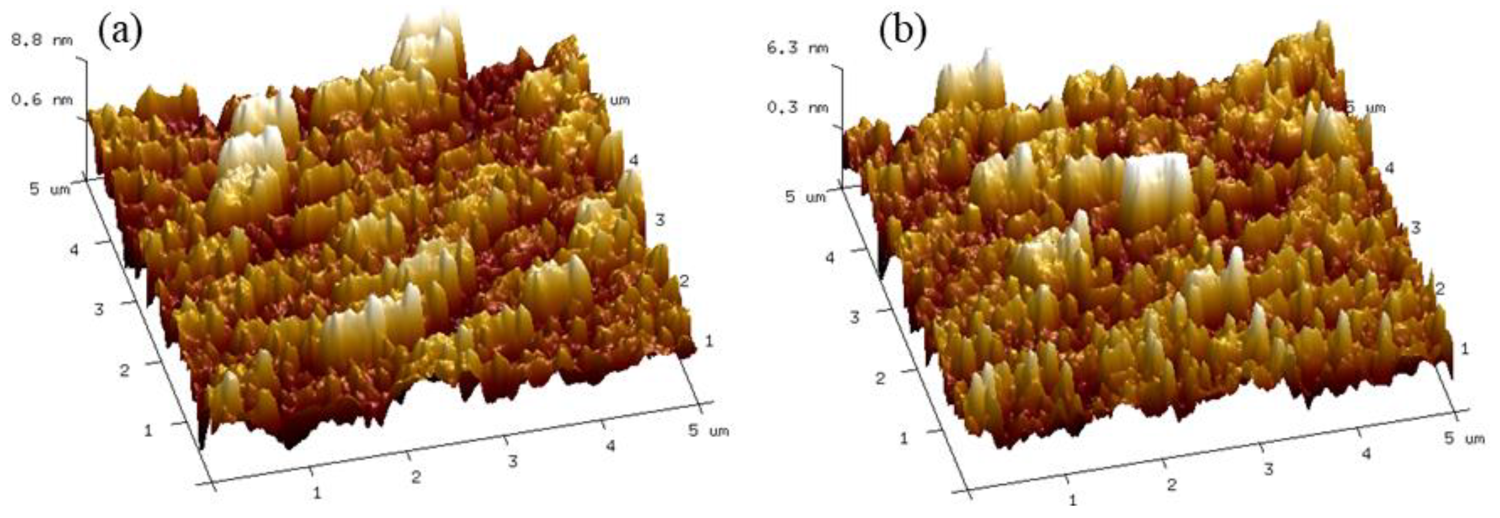
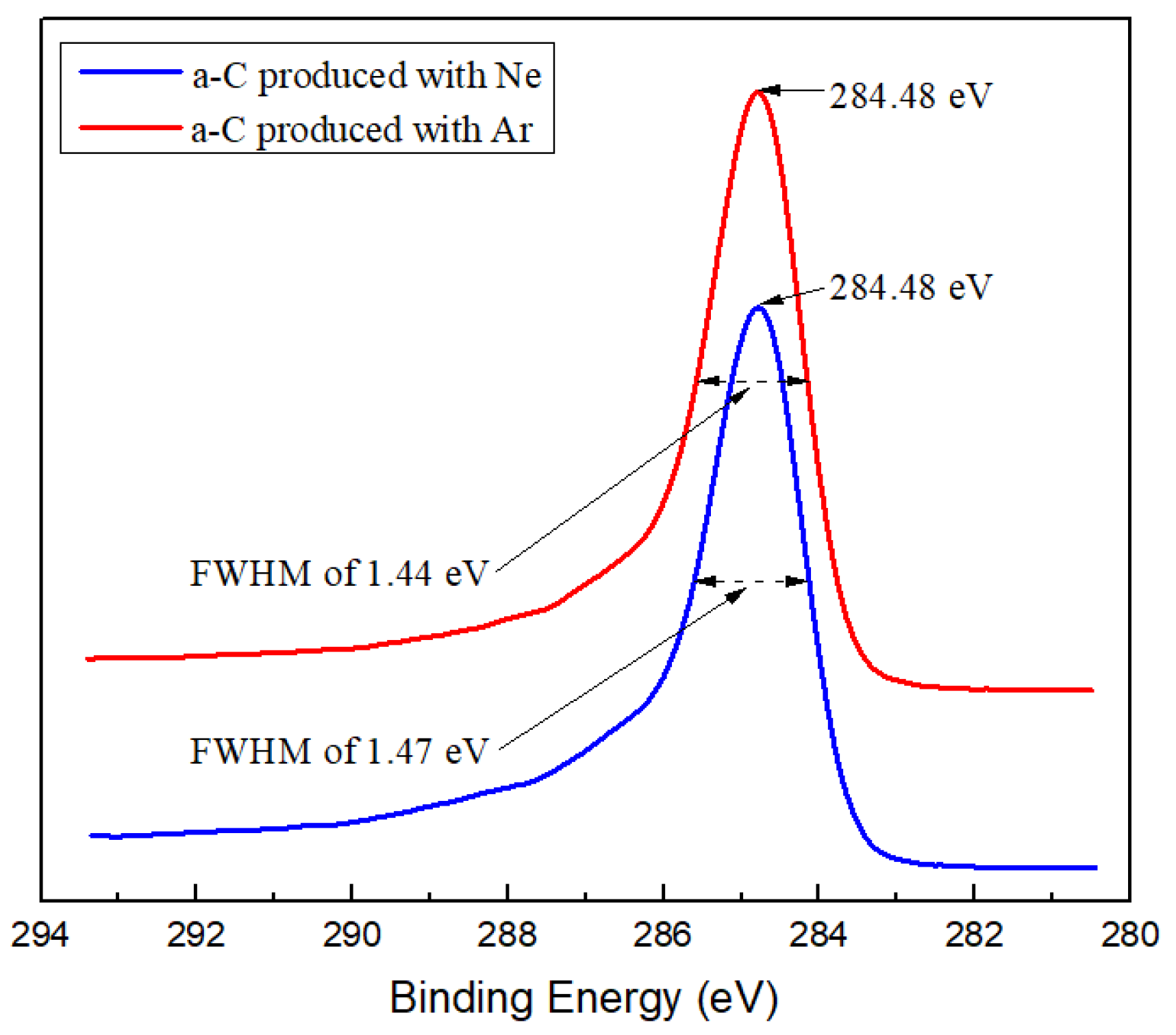
3.1. Microstructure Characterization

The surface morphology and cross-sectional images of the carbon thin films deposited with Ne and Ar are shown in Figure 2. The surfaces of both films comprise cauliflower-like clusters. However, the clusters produced by Ne are larger than those produced by Ar. In addition, the thickness of the a-C films produced by Ne is approximately 650 nm, whereas it is about 580 nm for those produced by Ar. Therefore, Ne yields higher deposition rate other than Ar.
The roughness of the coatings produced with two different discharge gases (Ar and Ne) has been quantitatively evaluated by AFM and the results are displayed in Figure 3. Amorphous carbon film sample with Ne atmosphere has an average roughness Ra of 1.77 nm with scanning range of 5 μm as presented in Figure 3a, while it is 1.08 nm for the one using Ar as discharge gas presented in Figure 3b. It is observed that the surface roughness of the amorphous carbon film deposited using Ne is 64% higher than the samples using Ar.
The roughness of the coatings usually has a great influence on SEY because the secondary electron can leave a smooth surface unhindered but with a rough surface it may be intercepted by surrounding walls [21].
A comparison for two typical XPS C1s spectra curves measured on the samples as-deposited with Ne and Ar is presented in Figure 4. It is clear that XPS peaks collected from the two thin films produced with Ne and Ar present similar geometrical characteristic. The binding energies of C1s are the same at 284.48 eV for both films deposited with Ne and Ar, the corresponding FWHMs are slightly different, of 1.47 eV for the former and 1.44 eV for the latter, respectively.
It is commonly assumed that carbon atoms in amorphous carbon films are sp3 and sp2 hybridized [22]. As shown in Figure 5, the line-shape of C1s curve can be fitted with five Gaussian functions, with the peaks at 284.6 eV (FWHM = 1.10 eV), 285.3 eV (FWHM = 1.20 eV), 286.0 eV (FWHM = 1.80 eV), 287.0 eV (FWHM = 1.80 eV) and 288.5 eV (FWHM = 1.80 eV) according to reference [23]. The peaks at 284.6 eV and 285.3 eV are related to sp2 and sp3 hybridized carbon bonds, respectively [24]. The two peaks at 286 eV and 287 eV are related to C-O and C=O bonds, respectively, which are mainly attributed to the adsorbed oxygen on the film surface. Besides, the peak at highest binding energy peaked at 288.5 eV is generally ascribed to π→π* transition [25]. The areas under the sp2 and sp3 peaks are used to determine their corresponding content from XPSPEAK software. The results are calculated as 72% sp2 content and 28% sp3 content for the amorphous carbon sample deposited using Ne. While the peak areas corresponding to sp2 and sp3 bonds are 68% and 32%, respectively, for the one produced with Ar. It can be observed that the sp2 content is slightly higher for the coatings using Ne, which results in larger FWHM of C1s peak.
Raman spectroscopy is a very effective technique to distinguish the microstructure of carbon materials well through different vibration modes and intensities. Figure 6 displays two typical Raman curves for the amorphous carbon films deposited with Ne and Ar. The Raman spectrum of the films shows two characteristic peaks at near 1360 cm−1 for the D peak and at near 1580 cm−1 for the G peak. The D peak is a zone edge A1g mode activated by disorder and the G peak is the zone center E2g mode of the single crystal graphite [26,27]. The D peak occurs only in disordered graphitic carbon and its intensity relative to the G mode (as measured by the ratio ID/IG) changes with the disorder. According to reference [27], the Raman spectrum data can be modeled based on a Breit-Wigner-Fano (BWF) profile for the G peak and a Lorentzian function for the D peak to extract the peak position, full width at half maximum (FWHM) and the intensity ratios of the carbon films. Raman spectrum fitting results are presented in Figure 6 by the dashed lines.
As shown in Figure 6, the disorder of the amorphous carbon coatings can be assessed by the ratio of the intensities of D and G peak as calculated by ID/IG. The corresponding data is summarized in Table 2. The ID/IG ratio of the sample produced with Ne is 1.036, while it is slightly lower at 1.0 for the sample deposited with Ar, suggesting higher sp2 hybridization content [28] in the film produced with Ne, which is in agreement with the analysis of the surface by XPS and the interpretation of the C1s line shape shown above.

3.2. SEY of Amorphous Carbon Films

The typical SEY (δ) curves measured on amorphous carbon film samples produced with Ne and Ar are shown in Figure 7. The δmax of the sample produced with Ar is 1.18, while it is 1.10 for Ne. In addition, Emax of the sample produce with Ne is 320 eV, while the other sample using Ar has an Emax value of 270 eV. All these differences might be explained based on the difference in surface roughness and composition. Rougher coatings generally lead to lower δmax and higher Emax [29]. When the secondary electrons emit from a rough surface, some of them will be recaptured by the surface leading to a lower SEY. Additionally, more primary electron energy is required for the corresponding excited secondary electrons to escape a rough surface other than a flat one. It is plausible by the pure geometric argument that for a fixed primary energy, an electron impinging on a tilted surface will penetrate less, if the depth is measured along the surface normal, than an electron impinging normally on a flat surface. Thus, to get the same average penetration on a rough surface that can be conceived as being composed of many small tilted surfaces, the primary electron must have higher energy. As a result, the SEY versus primary electron energy curve is shifted towards higher energies [30]. Besides, the higher sp3 hybridized bonds of the amorphous carbon coatings have a reduction effect on the Emax and increase the value of δmax. Therefore diamond-like carbon films with more sp3 hybridized bonds have a larger δmax close to 1.6 and a lower Emax at about 200 eV [31]. With higher sp3 hybridization content, the Emax of carbon coating deposited using Ar shifts to lower primary electron energy and δmax increases to 1.2, compared with that deposited in Ne.

4. Discussion

Generally, the SEY and its primary energy dependence is known to be influenced by the surface morphology and chemical composition. Hence the correlation between microstructural properties of the coatings and their SEY characteristic has been investigated by several methods (SEM, AFM, XPS and Raman Spectrum) and the results have been described in Section 3.
Amorphous carbon thin films deposited with Ne and Ar show columnar granularities with several tens of nanometers, as shown in Figure 2. From the AFM images (Figure 3), Ne gas induces rougher surface morphology of the a-C films. The use of Ne can reduce the kinetic energy of carbon atoms and reduce the mobility of the adatoms. The energy of sputtered carbon atom is obtained from the energy exchange with positive ions. Hence, the diffusion length of the carbon atoms on the surface is shortened [32,33]. The microstructure of thin films is related to the mobility of the adatoms during growth. When the secondary electrons emit from a rough surface, some of them will be recaptured by the surface leading to a lower SEY. In summary, such a surface produced with Ne can hinder the overflow of secondary electrons leading to a decreased secondary electron yield, which is consistent with the secondary electron measurement results.
It is well known that the properties of carbon materials are closely related to the sp2/sp3 ratio. The SEY of carbon coatings is usually related to the atomic hybridization states. Graphite and diamond are two well-known allotropes of carbon. Graphite purely consists of sp2 hybridized bonds, whereas diamond purely consists of sp3 hybridized bonds. Willis et al. [34] found that graphite has a low SEY and the sp2 structure shows a strong scattering effect. Hence, the secondary electrons reflection would take place due to their inelastic collision with carbon atoms, which changes the trajectory of the moving electrons. The electrons will lose their energy as a result of the collision, preventing the electrons passing through the barrier of overflow surface, thus reducing the SEY of the materials. According to the results published by Ascarelli et al. [35], diamond has a relatively large SEY and the scattering of sp3 hybridized bonds on electrons is weak. The surface of diamond has negative electron affinity due to its wide bandgap [36]. The smaller of the electronic affinity, the easier it is for electrons to escape. Consequently, electrons in diamond material are readily to move out of orbit and become secondary electrons at any time. The SEY of a-C films decreases with the increasing of sp2 bonds component.
One of the most common ways to characterize amorphous carbon is through the ratio of sp2 to sp3 hybridized bonds content in the thin films as described in Figure 5 and Figure 6. It is revealed that the sp2 hybridization is dominant in amorphous carbon films, which make the films more graphite-like than diamond-like. Actually, carbon materials with high sp3 domains are referred to as diamond-like carbon (owing to the similarity of many physical properties to those of diamond). Diamond-like carbon coatings have a large maximum SEY value closing to 1.6 [37]. The sp3 hybridized content of the thin films produced with Ar is higher, comparing with the samples deposited with Ne. It seems that argon favours sp3 bonds formation while depositing carbon thin films. Lifshitz et al. [38] proposed a “subplantation” model based on the energy of incident particles when depositing a tetrahedral amorphous carbon film (ta-C) with a C+ ion source. When the energies carried by the incident particles are low, the particles deposited on the substrate will be attached to the substrate in a nearly balanced state, the film is mainly sp2 hybridization structure; and when the energies of the incident particles are sufficiently high, the sp2 hybridized atoms in the thin film shift preferentially and aggregate to form sp3 structure. The ratio of the energies of Ne ion bombardment to Ar ion bombardment is calculated to be 0.71 according to Reference [33]. When using neon as sputtering gas, the deposited particles have a lower energy, hence a-C thin films with more sp2 hybrids will be formed. The maximum of SEY decrease for the coating deposited with Ne is probably ascribed to the increase of sp2 content. As a consequence, we concentrate on production of amorphous carbon films with more graphite-like structure to decrease SEY in the future work.
In this paper, It reveals that all the as-deposited amorphous carbon films have a δmax lower than 1.2 (threshold value calculated by simulations for SPPC) [39], much lower than the SEY of copper (which is 1.8), stainless steel (which is 2.5) and aluminum (which is 2.0) [40,41,42], which are common materials for the vacuum chambers of particle accelerators. It indicates that amorphous carbon thin film has inherent low SEY properties profiting by dominant sp2 hybridization content. Additionally, a-C film can decrease secondary electrons emission effectively and it is a potential surface coating for the suppression of electron-cloud in modern high-energy accelerators, such as SPPC.

5. Summary and Conclusions

Amorphous carbon thin films were produced by a DC magnetron sputtering system and SEY characterization was investigated in the National Synchrotron Radiation Laboratory. The experiment results showed that amorphous carbon thin film has low inherent SEY, compared with bare stainless-steel substrate. Hence a-C coating is considered to be a potential technique which is superior in cost and production for the suppression of electron cloud effect. Moreover, the amorphous carbon thin film does not require thermal activation, which means that it has great application prospects for vacuum chambers where baking is infeasbile and it can be a candidate for SPPC. The XPS data and Raman spectra indicate that amorphous carbon coatings deposited in Ne and Ar show more graphite-like than diamond-like behavior. The δmax of amorphous carbon coatings deposited in Ar is 1.18, while it reduces to 1.10 for Ne. The ratio of sp2 to sp3 hybridized bonds is larger for amorphous carbon coating produced in Ne, compared with amorphous carbon coatings produced in Ar. The increase of graphite-like structure is beneficial to decrease SEY. In addition, research on surface treatment to decrease the SEY of amorphous carbon coating is to be carried out in the future.

Author Contributions

Conceptualization, writing—original draft, writing—review and editing, Y.Z.; data curation, Y.W. (Yigang Wang); validation, methodology, S.W.; formal analysis, W.W.; data curation, X.G.; software, B.Z.; investigation, J.S.; Conceptualization, investigation, funding acquisition, project administration, Y.W. (Yong Wang). All authors have read and agreed to the published version of the manuscript.

Funding

This work was financially supported by the National Natural Science Foundation of China (Grant Nos. 11475166; 11575214).

Conflicts of Interest

The authors declare no conflict of interest.

References

  1. Cimino, R.; Demma, T. Electron cloud in accelerators. Int. J. Mod. Phys. A 2014, 29, 1430023. [Google Scholar] [CrossRef]
  2. Fukuma, H. Electron Cloud Observations and Predictions at KEKB, PEP-II and SuperB Factories. arXiv 2013, arXiv:1307.8330. [Google Scholar]
  3. Tobiyama, M.; Flanagan, J.W.; Fukuma, H.; Kurokawa, S.; Ohmi, K.; Win, S.S. Coupled bunch instability caused by an electron cloud. Phys. Rev. Spec. Top. Accel. Beams 2006, 9. [Google Scholar] [CrossRef] [Green Version]
  4. Iadarola, G.; Rumolo, G. Electron cloud in the CERN accelerators (PS, SPS, LHC). arXiv 2013, arXiv:1309.6795. [Google Scholar]
  5. Larciprete, R.; Cimino, R.; Commisso, M.; Grosso, D.R.; Flammini, R. The chemical origin of SEY at technical surfaces. arXiv 2013, arXiv:1308.1290. [Google Scholar]
  6. Romanov, G. Simulation of Multipacting with Space Charge Effect. Am. J. Phys. Appl. 2017, 5, 99–105. [Google Scholar] [CrossRef] [Green Version]
  7. Suetsugu, Y.; Fukuma, H.; Pivi, M.; Wang, L. Continuing study on electron-cloud clearing techniques in high-intensity positron ring: Mitigation by using groove surface in vertical magnetic field. Nucl. Instrum. Meth. Phys. Res. Sect. A 2009, 604, 449–456. [Google Scholar] [CrossRef]
  8. Suetsugu, Y.; Fukuma, H.; Shibata, K.; Kek, T.; Pivi, M.T.F.; Wang, L. Experimental Studies on Grooved Surfaces to Suppress Secondary Electron Emission. In Proceedings of the IPAC’10, Kyoto, Japan, 23–28 May 2010; pp. 2021–2023. [Google Scholar]
  9. Fischer, W.; Blaskiewicz, M.; Brennan, J.M.; Huang, H.; Hseuh, H.C.; Ptitsyn, V.; Roser, T.; Thieberger, P.; Trbojevic, D.; Wei, J.; et al. Electron cloud observations and cures in the Relativistic Heavy Ion Collider. Rev. Spec. Top. Accel. Beams 2008, 11, 041002. [Google Scholar] [CrossRef] [Green Version]
  10. Fukuma, H.; Flanagan, J.; Hosoyama, K.; Ieiri, T.; Kawamoto, T.; Kubo, T.; Suetake, A.; Uno, S.; Win, S.S.; Yoshioka, M. Status of solenoid system to suppress the electron cloud effects at the KEKB. In AIP Conference Proceedings; Chou, W., Mori, Y., Neuffer, D., Ostiguy, J.F., Eds.; American Institute of Physics: College Park, MD, USA, 2002; Volume 642, pp. 357–359. [Google Scholar]
  11. Vallgren, C.Y.; Arduini, G.; Bauche, J.; Calatroni, S.; Chiggiato, P.; Cornelis, K.; Pinto, P.C.; Henrist, B.; Metral, E.; Neupert, H.; et al. Amorphous carbon coatings for the mitigation of electron cloud in the CERN Super Proton Synchrotron. Phys Rev Spec Top. Accel. Beams 2011, 14, 071001. [Google Scholar] [CrossRef]
  12. Gompel, M.V.; Pinto, P.C.; Vollenberg, W.; Chiggiato, P.; Cruikshank, P.; Pasquino, C.C.; Sapountzis, A.; Taborelli, M.; Espinos, J.P. Amorphous Carbon Thin Film Coating of the SPS Beamline: Evaluation of the First Coating Implementation. In Proceedings of the IPAC’17, Geneva, Switzerland, 14–19 May 2017; pp. 44–47. [Google Scholar]
  13. Salemme, R.; Baglin, V.; Bregliozzi, G. Amorphous carbon coatings at cryogenic temperatures with LHC type beams: First results with the COLDEX experiment. In Proceedings of the IPAC’15, Richmond, VA, USA, 3–8 May 2015; pp. 3112–3114. [Google Scholar]
  14. Salemme, R.; Baglin, V.; Bregliozzi, G.; Chiggiato, P. Vacuum Performance of Amorphous Carbon Coating at Cryogenic Temperature with Presence of Proton Beams. In Proceedings of the IPAC’16, Busan, Korea, 8–13 May 2016; pp. 3663–3666. [Google Scholar]
  15. Nishiwaki, M.; Kato, S. Study of the secondary electron yield of carbon materials. J. Vac. Soc. Jpn. 2005, 118, 48. [Google Scholar]
  16. Woods, M.E.; Hopkins, B.J.; Matthews, G.F.; McCracken, G.M.; Sewell, P.; Fahrang, H. An investigation of the secondary-electron emission of carbon samples exposed to a hydrogen plasma. J. Phys. D Appl. Phys. 1987, 20, 1136–1142. [Google Scholar] [CrossRef]
  17. Ripalda, J.M.; Montero, I.; Vazquez, L.; Raboso, D.; Galan, L. Secondary electron emission and photoemission studies on surface films of carbon nitride. J. Appl. Phys. 2006, 99, 043513. [Google Scholar] [CrossRef] [Green Version]
  18. Alfonso, E.; Olaya, J.; Cubillos, G. Thin film growth through sputtering technique and its applications. In Crystallization-Science and Technology; Andreeta, M.R.B., Ed.; IntechOpen: Rijeka, Croatia, 2012. [Google Scholar]
  19. Gou, L.; Qi, C.S.; Ran, J.G.; Zheng, C.Q. SiC film deposition by DC magnetron sputtering. Thin. Solid Films 1999, 345, 42–44. [Google Scholar] [CrossRef]
  20. Jung, H.S.; Park, H.H.; Mendieta, I.R.; Smith, D.A. Enhancement of sp3 hybridized C in amorphous carbon films by Ar ion bombardment and Si incorporation. J. Appl. Phys. 2003, 94, 4828–4834. [Google Scholar] [CrossRef]
  21. Bruining, H. Physics and Applications of Secondary Electron Emission; Pergamon Press: Oxford, UK, 1954; pp. 70–96. [Google Scholar]
  22. Comelli, G.; Stoehr, J.; Robinson, C.J.; Jark, W. Structural studies of argon-sputtered amorphous carbon films by means of extended x-ray-absorption fine structure. Phys. Rev. B 1988, 38, 7511–7519. [Google Scholar] [CrossRef]
  23. Diaz, J.; Paolicelli, G.; Ferrer, S.; Comin, F. Separation of the sp3 and sp2 components in the C1s photoemission spectra of amorphous carbon films. Phys. Rev. B 1996, 54, 8064–8069. [Google Scholar] [CrossRef]
  24. Merel, P.; Tabbal, M.; Chaker, M.; Moisa, S.; Margot, J. Direct evaluation of the sp3 content in diamond-like-carbon films by XPS. Appl. Surf. Sci. 1998, 136, 105–110. [Google Scholar] [CrossRef]
  25. Jackson, S.T.; Nuzzo, R.G. Determining hybridization differences for amorphous carbon from the XPS C1s envelope. Appl. Surf. Sci. 1995, 90, 195–203. [Google Scholar] [CrossRef]
  26. Robertson, J.F.R. Diamond-like amorphous carbon. Mater. Sci. Eng. R Rep. 2002, 37, 129–281. [Google Scholar] [CrossRef] [Green Version]
  27. Ferrari, A.C.; Robertson, J. Interpretation of Raman spectra of disordered and amorphous carbon. Phys. Rev. B 2000, 61, 14095–14107. [Google Scholar] [CrossRef] [Green Version]
  28. Ferrari, A.C.; Robertson, J. Resonant Raman spectroscopy of disordered, amorphous, and diamondlike carbon. Phys. Rev. B 2001, 64, 075414. [Google Scholar] [CrossRef] [Green Version]
  29. Kunz, C. Synchrotron radiation: Overview. In Photoemission in Solids II; Ley, L., Cardona, M., Eds.; Springer: Berlin/Heidelberg, Germany, 1979; Volume 27, pp. 299–348. [Google Scholar]
  30. Nishimura, K.; Itotani, T.; Ohya, K. Influence of Surface Roughness on Secondary Electron Emission and Electron Backscattering from Metal Surface. Jpn. J. Appl. Phys. 1994, 33, 4727–4734. [Google Scholar] [CrossRef]
  31. Yin Vallgren, C.; Chiggiato, P.; Costa Pinto, P.; Neupert, H.; Rumolo, G.; Shaposhnikova, E.; Taborelli, M.; Kato, S. Performance of carbon coatings for mitigation of electron cloud in the SPS. In Proceedings of the IPAC’11, San Sebastián, Spain, 4–9 September 2011; pp. 1590–1592. [Google Scholar]
  32. Ellmer, K.; Hinze, J.; Klaer, J. Copper indium disulfide solar cell absorbers prepared in a one-step process by reactive magnetron sputtering from copper and indium targets. Thin. Solid Films 2002, 413, 92–97. [Google Scholar] [CrossRef]
  33. Wasa, K.; Adachi, H.; Kitabatake, M. Thin Film Materials Technology: Sputtering of Compound Mater; Springer: Berlin/Heidelberg, Germany, 2004. [Google Scholar]
  34. Willis, R.F.; Fitton, B.; Painter, G.S. Secondary-electron emission spectroscopy and the observation of high-energy excited states in graphite: Theory and experiment. Phys. Rev. B 1974, 9, 1926–1937. [Google Scholar] [CrossRef]
  35. Ascarelli, P.; Cappelli, E.; Pinzari, F.; Rossi, M.C.; Salvatori, S.; Merli, P.G.; Migliori, A. Secondary electron emission from diamond: Physical modeling and application to scanning electron microscopy. J. Appl. Phys. 2001, 89, 689–696. [Google Scholar] [CrossRef]
  36. Pan, L.S.; Kania, D.R. Diamond: Electronic Properties and Applications; Springer: New York, NY, USA, 1995; pp. 50–60. [Google Scholar]
  37. Nishiwaki, M.; Kato, S. Residual gas analysis and electron cloud measurement of DLC and TiN coated chambers at KEKB LER. In Proceedings of the IPAC’10, Kyoto, Japan, 23–28 May 2010; pp. 3852–3854. [Google Scholar]
  38. Lifshitz, Y.; Kasi, S.R.; Rabalais, J.W.; Eckstein, W. Subplantation model for film growth from hyperthermal species. Phys. Rev. B 1990, 41, 10468–10480. [Google Scholar] [CrossRef]
  39. Tang, J.; Berg, J.S.; Zheng, S.; Han, T.; Liu, B.; Gupta, R.; Ruan, M.; Chou, W.; Yuan, Y.; Sun, B.; et al. Concept for a future Super Proton-Proton Collider. arXiv 2015, arXiv:1507.03224. [Google Scholar]
  40. Hartung, W.H.; Conway, J.; Dennett, C.A.; Greenwald, S.; Kim, J.S.; Li, Y.; Moore, T.P.; Omanovic, V. Measurements of secondary electron yield of metal surfaces and films with exposure to a realistic accelerator environment. In Proceedings of the IPAC’13, Shanghai, China, 12–17 May 2013; pp. 3493–3495. [Google Scholar]
  41. Hartung, W.H.; Asner, D.M.; Conway, J.V.; Dennett, C.A.; Greenwald, S.; Kim, J.S.; Li, Y.; Moore, T.P.; Omanovic, V.; Palmer, M.A.; et al. In-situ measurements of the secondary electron yield in an accelerator environment: Instrumentation and methods. Nucl. Instrum. Meth. A 2015, 783, 95–109. [Google Scholar] [CrossRef] [Green Version]
  42. Kirby, R.E.; King, F.K. Secondary electron emission yields from PEP-II accelerator materials. Nucl. Instrum. Meth. A 2001, 469, 1–12. [Google Scholar] [CrossRef]
Figure 1. Schematic diagram of secondary electron yield test.
Coatings 10 00884 g001
Figure 2. (a,c) Surface and (b,d) Cross-sectional images of the amorphous carbon films deposited with different discharging gases (a,b) Ne, (c,d) Ar.
Coatings 10 00884 g002
Figure 3. This The 3D atomic force microscopy (AFM) images of the samples produced with various sputtering gases (a) Ne (b) Ar.
Coatings 10 00884 g003
Figure 4. C1s lines of amorphous carbon coatings obtained with Ne and Ar.
Coatings 10 00884 g004
Figure 5. X-ray photoelectron spectroscopy C1s spectra of a-C coatings deposited with (a) Ne and (b) Ar, fitted by five Gaussian functions.
Coatings 10 00884 g005
Figure 6. Raman spectra measured on the amorphous carbon thin film deposited by (a) Ne and (b) Ar. The Raman spectrum is fitted by a Breit-Wigner-Fano line shape and a Lorentzian line shape.
Coatings 10 00884 g006
Figure 7. The SEY curves as a function of primary energy for amorphous carbon coatings produced with various working gases Ne (blue line) and Ar (red line).
Coatings 10 00884 g007
Table 1. Parameters of DC magnetron sputtering for amorphous carbon thin films.
ParameterUnitValue
Sputtering Gas-Ne, Ar
PowerW250
Pressurembar3.8 × 10−2
Magnetic FieldGauss150
Gas Flowsccm5
Table 2. The parameters of the C Raman spectra in a-C films.
Sputtering ConditionsD Peak
(cm−1)
G Peak
(cm−1)
ID/IG
Ne Gas135015801.036
Ar Gas134915861.0

