Article

Fabrication of Ultralow Stress TiO2/SiO2 Optical Coatings by Plasma Ion-Assisted Deposition

1
Institute of Optics and Electronics, Chinese Academy of Sciences, Chengdu 610209, China
2
Key Laboratory of Optical Engineering, Chinese Academy of Sciences, Chengdu 610209, China
*
Author to whom correspondence should be addressed.
Coatings 2020, 10(8), 720; https://doi.org/10.3390/coatings10080720
Submission received: 28 June 2020 / Revised: 14 July 2020 / Accepted: 21 July 2020 / Published: 23 July 2020

Abstract

:
Optical and mechanical properties of multilayer coatings depend on the selected layer materials and the deposition technology; therefore, knowledge of the performances of thin films is essential. In the present work, titanium dioxide (TiO2) and silicon dioxide (SiO2) thin films have been prepared by plasma ion-assisted deposition (PIAD). The optical, structural, and mechanical properties of thin films have been investigated using spectrometer/ellipsometer, X-ray diffraction (XRD), atomic force microscopy (AFM), and laser interferometer. The results show that TiO2 film fabricated by PIAD induces a high refractive index, wide optical band gap, amorphous structure, smooth surface, and tensile stress. In the case of SiO2 film, high bias voltage leads to dense structure and compressive stress. As an application, a three-wavelength high reflectance at 632.8, 808, and 1550 nm was optimized and deposited. The dependence of total stress in the multilayer on the substrate temperature was studied as well. In conclusion, it was demonstrated that PIAD is an effective method for the preparation of ultralow stress TiO2/SiO2 multilayer films. The achieved stress was as low as 1.4 MPa. The result could provide guidance to the stress optimization of most optical components without prefiguring, backside coating, and postdeposition treatments.

Graphical Abstract

1. Introduction

High-performance components for precision-optics applications require thin films with perfect optical properties, as well as minimal mechanical stress. As a result, it is crucial to select the coating materials and the deposition technology very carefully. In general, metal oxides (SiO2, Al2O3, HfO2, Ta2O5, Nb2O5, and TiO2) and metal fluorides (MgF2 and Na3AlF6) are common layer materials applied for coating design in the visible and near-infrared spectral range. Conventional electron-beam evaporation (EBE) remains the preferred vacuum coating technology for nanosecond pulsed laser devices [1,2]. Plasma ion-assisted deposition (PIAD) and magnetron sputtering (MS) have been successfully employed for femtosecond laser systems [3,4]. Meanwhile, ion-beam sputtering (IBS) has been comprehensively demonstrated for the preparation of high reflectivity and ultralow-loss films in the advanced gravitational waves interferometers [5,6]. With the development of vacuum-coating technology, the complexity of thin films has significantly increased, and mechanical stress control has become a major challenge. Excessive stress can cause delamination, deformation, or cracks, severely affecting the properties and the stability of thin-film devices [7,8,9,10]. Therefore, the optimization of mechanical stress is very much necessary for the better performance of optical coatings.
The tensive or compressive stresses in thin films depend on many factors, such as deposition technique [11], substrate material [12], substrate temperature during preparation [9], layer material [7], deposition rate [13], work gas pressure [14], etc. Up to now, several methods have been applied to manipulate the mechanical stress of thin films. Firstly, the substrate can be pretreated to an opposite surface figure either during the polishing process or before coating with a special nonuniform matching layer, so that prefiguring the coated surface can offset the net effect of film stress [15,16]. In principle, these approaches need to determine the stress characteristics of optical coatings in advance, and preprocessing the optical surface is challenging for an optical element with complex geometry. Secondly, layer materials with opposite stress can be employed to decrease the multilayer stress, although the available materials are very limited [7,11]. Thirdly, backside coatings and thermal annealing treatment have been commonly used to control stress-induced deformation, the corresponding operation and disadvantage of the approaches are reviewed in other literature [4,11,13,17,18,19,20]. Besides, thermal oxide patterning and ion implantation have been successfully used to compensate film stress in thin silicon substrates for X-ray optical applications [21,22]. Nevertheless, the methods have limitations as well. Last but not least, since thin films fabricated by EBE and PIAD can be manipulated as tensile or compressive stress [7,23,24], the films prepared using MS and IBS are commonly compressive stress [9,11,17]. It is possible to realize stress control by combining several coating technologies. Tajima et al. [23] have studied the stress control of SiO2 film by simultaneous sputtering and EBE. As a result, the obtained stress of SiO2 film prepared with the proposed method is approximately 60% of that by EBE and one-fourth of that by sputtering. Woo et al. [24] have reported the stress optimization for a TiO2/MgF2 narrow band-pass filter. The destructive tensile stress in the EBE MgF2 films can be counteracted by the compressive stress of the PIAD TiO2 films, consequently without microcracks in the multilayer. Liu et al. [25] have investigated the stress compensation for antireflection coating, which is designed and fabricated with IBS SiO2 and atomic layer deposition Al2O3. Finally, the stress is as low as 38 MPa. Taking the efficiency and cost of stress-control technology, as well as the optical and environmental stability of optical coatings into consideration, PIAD is still the best choice for the preparation of ultralow stress films.
In the present work, titanium dioxide (TiO2) and silicon dioxide (SiO2) have been chosen for the optical coatings due to the high refractive index contrast, which can simplify the optical design, then reduce the residual stress. Single layers of TiO2 and SiO2 as well as a three-wavelength high reflection (HR) are prepared by PIAD. Detailed results for the optical, mechanical, and environmental properties are characterized and discussed. It suggests that thin films having perfect optical performance and ultralow stress can be realized with the optimization of the deposition parameters.

2. Materials and Methods

TiO2 and SiO2 films were prepared by a SYRUS pro 1110 DUV vacuum system (Leybold, Alzenau, Germany), consisting of an advanced plasma source (APS), two electron beam guns, and four ceramic heaters. The APS was used to bombard a growing film with argon (Ar) and oxygen (O2) ions. In the coating process, a base pressure approximately 2.0 × 10⁻⁴ Pa was ensured in the vacuum chamber by a cryopump set. Fused silica plates and silicon wafers with a root-mean-square surface roughness of approximately 0.5 nm were used as the substrates. The distance between the evaporation source and the substrate was approximately 750 mm. Before the deposition, substrates were first treated manually with alcohol and acetone in a standard laboratory environment. Then, they were cleaned with Ar plasma formed by the APS in the vacuum chamber to remove potential contaminations. High-purity Ti3O5 and SiO2 grains (Merck, Darmstadt, Germany) were used as starting materials. The physical thickness and deposition rate of thin films were controlled by a quartz-crystal monitor, which was positioned at the top center of the deposition chamber. TiO2 and SiO2 were fabricated by the PIAD at a substrate temperature of 180 °C. The deposition rates of TiO2 and SiO2 films were set to 0.2 and 0.4 nm/s, respectively, and the thickness of the TiO2 and SiO2 films was kept at about 350 and 900 nm. High purity O2 (99.999%) was employed to improve the stoichiometric ratio of the thin films. The plasma source is set to constant bias voltage and discharge current mode. Further details for the deposited TiO2 and SiO2 films were summarized in Table 1. After the deposition processes were finished, the samples were allowed to cool down to room temperature, and the vacuum chamber was vented.
The TiO2 film on fused silica substrate was applied for the transmittance, thickness, optical constants, and energy band-gap analysis. A Perkin Elmer Lambda 1050 spectrophotometer (Waltham, MA, USA) was used to measure the transmittance of TiO2 film at a normal incident angle. SiO2 film on silicon substrate was employed for thickness and refractive index determination with a variable-angle spectroscopic ellipsometer (VASE, J.A. Woollam Co., Inc., Lincoln, NE, USA). The ellipsometric data were characterized at angles of incidence 65°, 70°, and 75°. The samples deposited on fused silica substrates were also used to analyze the microstructure, surface morphology, and stress of the TiO2 and SiO2 films. Microstructures of thin films were investigated with a X’Pert3 Powder X-ray diffraction (XRD, PANalytical, Almelo, The Netherlands) operated with Cu-Kα radiation (λ = 0.154 nm) in symmetrical Φ-2Φ geometry. The incident angle ranged from 10° to 80° with a step of 0.03°. The surface morphology was examined through a Veeco Dimension 3100 atomic force microscopy (AFM, Veeco, Santa Barbara, CA, USA), performing in a tapping mode for an imaging surface with 5 μm × 5 μm and 5 μm × 5 μm sample points. A Zygo laser interferometer (GPI-XP, Middlefield, CT, USA) was used to evaluate the stress of TiO2 and SiO2 films by measuring the variation in curvatures of the substrate before and after deposition. The measurements were performed at the He-Ne laser wavelength (λ = 632.8 nm). The measurement accuracy of the optical interferometer was better than λ/100 for the surface flatness.

3. Results and Discussion

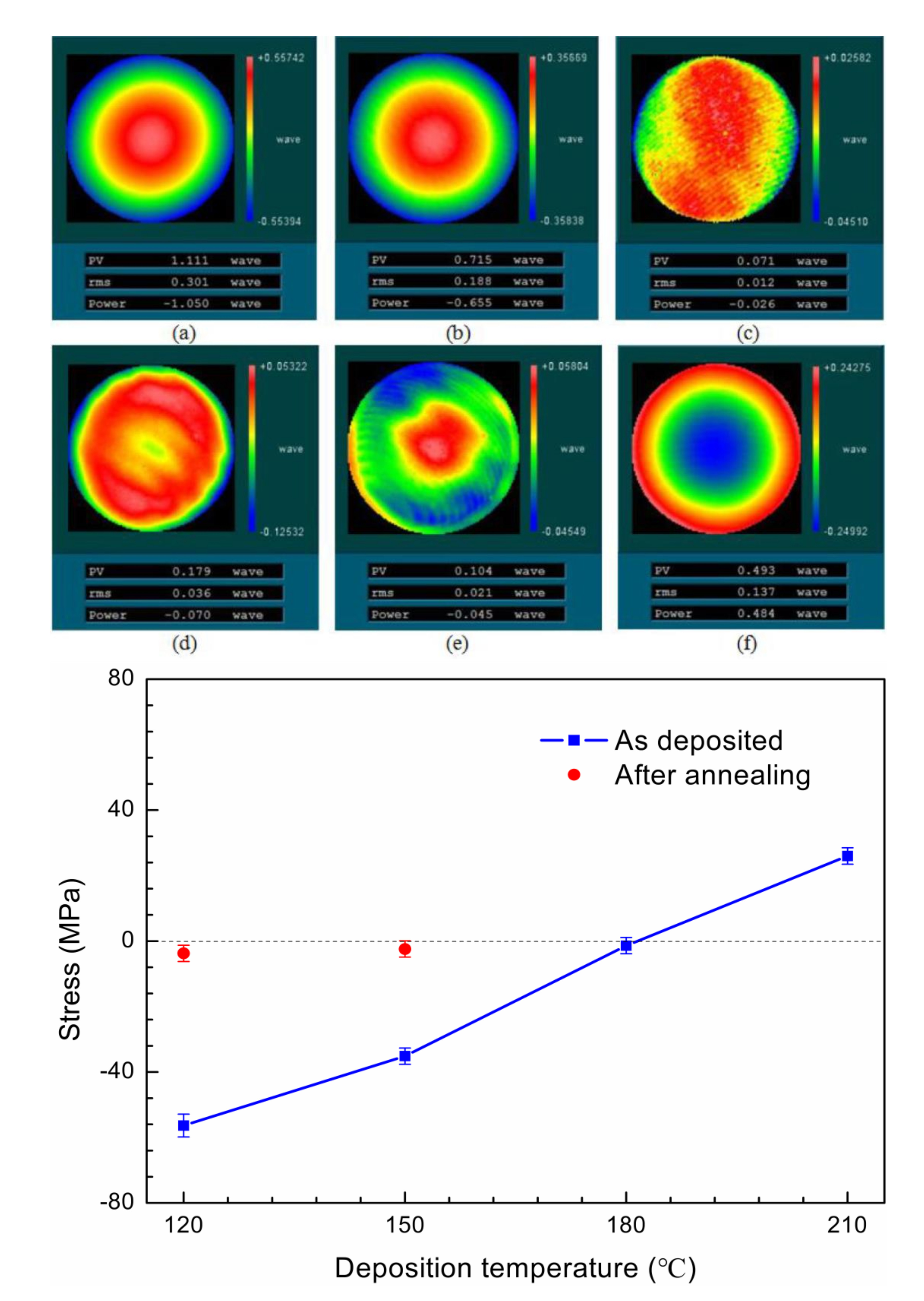
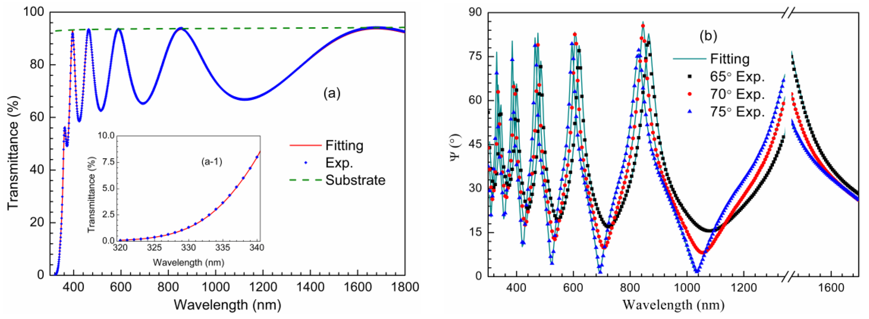
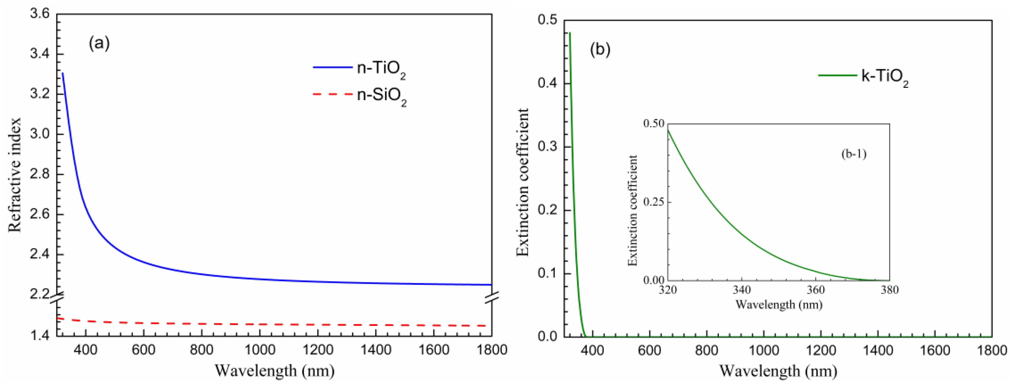
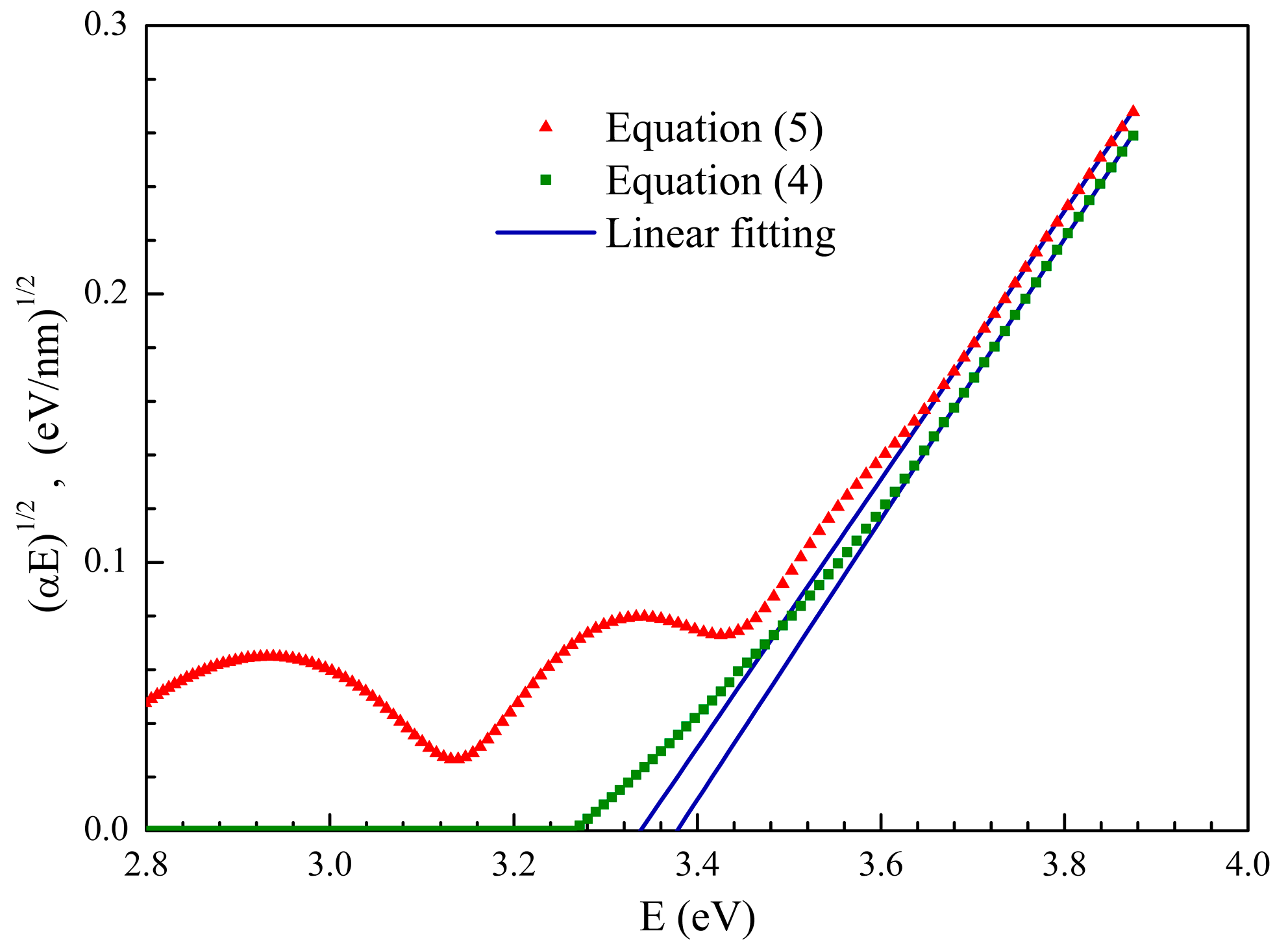
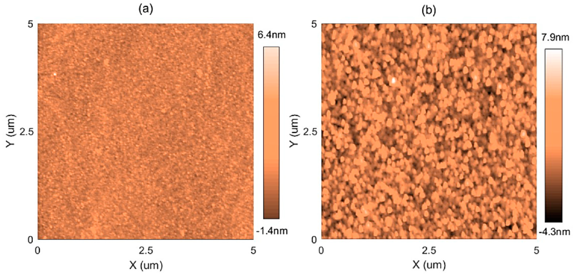
3.1. Single-Layer Coatings

To fabricate multilayer coatings with optimizing optical and mechanical properties, it was necessary to investigate the performances of the deposited TiO2 and SiO2 single layers. The physical thickness and optical constants (n, k) of the TiO2 film were determined from a spectrophotometric measurement. Transmittance spectra of the TiO2 film and fused silica substrate in the range of 300–1800 nm with a 1 nm wavelength step were obtained by the PE Lambda 1050 spectrophotometer, as presented in Figure 1a. The transmittance spectrum of TiO2 film was lower than that of the substrate, meaning that the refractive index of TiO2 film was higher than that of the substrate. The transmittance maxima of TiO2 film were consistent with that of the substrate above 400 nm. It indicated that the TiO2 film is a negligible-absorption and refractive-index, homogeneous layer in the visible and near-infrared range. At shorter wavelengths, the spectrum deviation between TiO2 film and substrate was caused by the absorption of TiO2 film. In addition, fused silica was a transparent substrate in the relevant wavelength range. It had been well polished and had sufficient thickness to avoid surface interference on the spectral measurement. The transmission of a single-layer absorbing film is a function of the refractive index (n), extinction coefficient (k), physical thickness (d), and the wavelength of light (λ). In our characterization process, the functional forms of n(λ) and k(λ) were described by the Tauc-Lorentz model [26]. The imaginary part (ε2) of the complex dielectric function ε = ε 1 i ε 2 = ( n i k ) 2 is defined by:
ε 2 ( E ) = { A E 0 Γ ( E E g ) 2 ( E 2 E 0 2 ) 2 + Γ 2 E 2 1 E , E > E g 0 , E E g
where A, E0, Eg, and Γ denote amplitude, peak transition energy, band-gap energy, and broadening parameter, respectively. E = hc/λ is photon energy, h and c represent the Planck’s constant and the velocity of light in vacuum. The real part (ε1) of the dielectric function is achieved using analytical integration of the Kramers–Krönig relation:
ε 1 ( E ) = ε + 2 π ( C . P . ) 0 ξ ε 2 ( ξ ) ξ 2 E 2 d ξ
where (C.P.) denotes the Cauchy principal value of the integral. ε represents the contribution of the optical transition at higher energies. The constants d, A, E0, Γ, Eg, and ε are fitting parameters. The fitting was then performed by minimizing the squared difference between the experimentally measured and calculated transmittance values. The optimal-selection approach of these parameters was carried out using the particle swarm optimization algorithm [27]. After a fine adjustment of the settings, a proper fitting could be obtained, and then the optical constants and thickness of thin film were determined.
The experimental and calculated transmittances were in good agreement, as exhibited in Figure 1a. The average discrepancies at wavelengths shorter than 400 nm were ~0.45%, ~0.15% in the entire wavelength range. It was demonstrated that the Tauc-Lorenz model gives good results in the determination of optical constants of the TiO2 film near the cut-off wavelength. The best-fitting thickness of the TiO2 film was 372.9 nm, listed in Table 2. The values of the parameters in the Tauc-Lorentz expressions Equations (1) and (2) were A = 193.29 eV, E0 = 4.47 eV,  = 1.60 eV, Eg = 3.24 eV, and ε = 1.86. The obtained wavelength dependence of the refractive index is shown in Figure 2a by the solid curve. The refractive index at 500 nm was 2.436. As expected, the refractive index of the TiO2 film deposited by PIAD was larger than that of EBE (2.358) and smaller than that of IBS (2.508) [28,29]. It was not surprising that the higher the deposition energy, the denser the film structure and the greater the refractive index.
Moreover, the optical band gap of the TiO2 film was calculated with the help of Tauc plots. For indirect band gap, the absorption coefficient α is a function of the photon energy E in the following equation [30]:
α ( E ) = B ( E E g ) 2 E
where B is a fitting constant. From Equation (3), it can be seen that (αE)1/2 has a linear dependence on E. Thus, by plotting (αE)1/2 versus E, the optical band gap Eg could be determined from extrapolating the linear fit to zero. The absorption coefficient was calculated through extinction coefficient k(λ):
α = 4 π λ k ( λ )
The extinction coefficient k(λ) was obtained from spectrophotometric measurement. On the other hand, in a high-absorption spectral range, the absorption coefficient α is related to the transmittance T and physical thickness d of thin-film based on Beer’s law [29]:
α 1 d ln ( 1 T )
In order to reduce the influence of spectral measurement error on the accuracy of the calculated coefficients, the transmittance spectrum near the cutoff edge (above 0.1%) was applied to the determinations of the absorption coefficient and extinction coefficient. In Figure 3, the Tauc plots for the indirect band gap and the corresponding linear fits for the TiO2 film deposited by PIAD are presented. The optical band gaps linear fitted using Equations (4) and (5) were 3.38 and 3.34 eV, respectively. They were quite close to each other, which was due to the successful application of the Tauc-Lorentz model for the parameterization of the optical constants of thin film near the absorption edge. As shown in the illustration in Figure 1a, the deviation between the experimental and calculated transmittances was less than 0.1% in the wavelength range from 320 to 340 nm. The result can be considered as the accuracy of optical band gap determination in this investigation. In general, the optical band energies obtained by Equations (4) and (5) are commonly larger than that determination from the Tauc-Lorentz model.
For the SiO2 film, it was difficult to directly investigate a single layer deposited on the fused silica substrate since there was no refractive index contrast and no variation in transmittance with respect to the wavelength. To overcome the problem, a considerable difference in transmission could be achieved with a double-layer structure consisting of a thin TiO2 layer and thick SiO2. As expected, the thickness and refractive index of SiO2 film could be estimated by fitting the transmission curve with commercial software like OptiRE [31]. The method had been introduced in detail in the previous research paper [32]. Besides, ellipsometric measurement was an excellent choice to determine the parameters of the SiO2 film deposited on Si substrate [33]. In this case, the reflection ellipsometry data were characterized in the range of 300–1700 nm using the VASE. The data analysis was performed with a reasonable assumption. The SiO2 film was treated to be non-absorbing, as the extinction coefficient is lower than 1.0 × 10⁻⁴ in the interesting wavelength range and had a negligible impact on the ellipsometry data. The ellipsometric parameters Ψ and Δ were simultaneously fitted with thickness and refractive index. Wavelength dependency of SiO2 refractive index is described by Sellmeier:
n 2 = 1 + A 1 ( λ / λ 0 ) 2 ( λ / λ 0 ) 2 A 2 + A 3 ( λ / λ 0 ) 2 ( λ / λ 0 ) 2 A 4 + A 5 ( λ / λ 0 ) 2 ( λ / λ 0 ) 2 A 6
where A1, …, A6 are dimensionless parameters, λ0 = 1000 nm, the unit of λ is nanometer. Figure 1b shows the experimental Ψ data and the best-fit curves of the SiO2 single layer at angles of incidence 65°, 70°, and 75°. It can be seen that the measured data are well fitted with the method. The thickness of the SiO2 film is characterized by 936.7 nm. The determining refractive index of SiO2 film is presented in Figure 2a with the dashed line. The parameters in the Sellmeier expressions are A1 = 4.842825, A2 = 1.332323, A3 = 6.650996, A4 = 2.796139, A5 = 100.0728, and A5 = 1275.594. For the SiO2 film deposited by PIAD at the 140 V bias voltage, the refractive index at 500 nm, which was larger than that of fused silica substrate (1.4623), was equal to 1.477.
Figure 4 presents the XRD patterns of thin films deposited on fused silica substrates. The absence of any sharp diffraction peaks and the presence of hump indicated the amorphous phase of the TiO2 and SiO2 films prepared by PIAD technology at the substrate temperature of 180 °C. The surface morphologies of thin films were investigated by AFM over 5 μm × 5 μm areas. Figure 5 shows typical morphologies of the TiO2 and SiO2 films. The RMS roughness of the surface was calculated by the definition [30]:
RMS = i = 1 N ( z i z a v g ) 2 N 1
where zi is the current value of z, zavg is the average value of z on the scanned area, and N is the number of points in the image. Experimentally, the RMS roughness of TiO2 and SiO2 films were determined to 0.52 and 1.39 nm, respectively. It is exhibited that the surface roughness of TiO2 film is smaller than that of SiO2 film attributed to the larger physical thickness of the latter.
Stress measurements of the TiO2 and SiO2 single layers were carried out with a Zygo laser interferometer by characterizing the reflected wave-front deformation of fused silica substrates. The stress of thin film was calculated by the Stoney equation [34]:
σ = E s t s 2 6 ( 1 ν s ) d f ( 1 R 1 1 R 0 )
R D 2 8 P
where, Es and νs are Young’s modulus and Poisson’s ratio of the substrate, ts and df are the thicknesses of the substrate and deposited thin film, and R0 and R1 are the radii of curvatures of the substrate before and after deposition. P is the power of reflected wave-front mapping, D is the diameter of the clear aperture. In the present work, the nominal thickness and diameter of fused silica substrates were 3 and 40 mm. Es and νs of fused silica were 72 GPa and 0.17. For the preparation of TiO2 and SiO2 films, the measured variations of reflected wave-front mapping were determined and are presented in Figure 6. It can be seen that after the deposition of 372.9 nm TiO2 and 936.7 nm SiO2 films, the power values of the reflected wave-fronts of these substrates were changed with 0.151 and −0.911λ (λ = 632.8 nm). Accordingly, the calculated stresses of the TiO2 and SiO2 films from Equations (8) and (9) were +164.8 and −395.8 MPa. Here, positive and negative stress values represent tensile and compressive stress, respectively. As demonstrated in [7,20,35], when the thin film is taken out of the deposition chamber, the adsorption of water can lead to a strong evolution of the stress over time. Thereby, it is important to keep in mind that thin film should be stored in a normal laboratory environment for a long time. Then the surface figure is measured to obtain the final stable stress behavior. The stress data presented in this work were measured after at least four weeks of storage if there is no other statement.

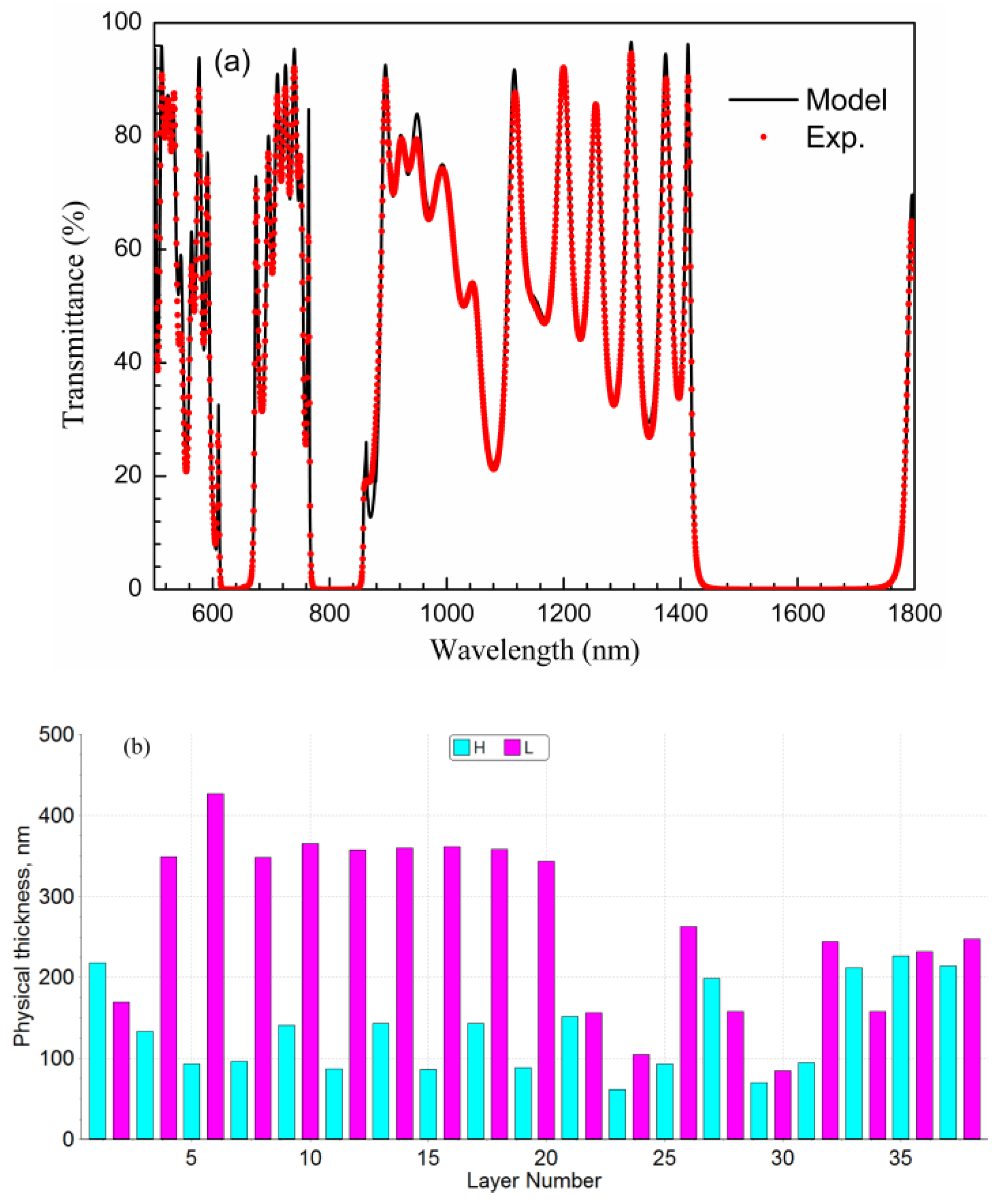
3.2. Multilayer Coatings

Based on the results of TiO2 and SiO2 films, a three-wavelength HR was optimized and fabricated on the fused silica substrate. For the multilayer coating design, the performance target was reflectivity greater than 99.95% at wavelengths of 632.8, 810, and 1550 nm. Taking into consideration the feasibility and repeatability, each working wavelength had a band with a width of at least 30 nm. To obtain better environmental durability, the outermost layer of optical coatings was SiO2 with a thickness of at least 200 nm. The structure of the three-wavelength HR is optimized with the help of a needle technique incorporated into the OptiLayer software (version 13.77f) [31]. The theoretical transmission spectrum and layer thickness profile of the final 38-layer coating design are exhibited in Figure 7. The total thicknesses are 3020.51 nm for TiO2 material and 3802.26 nm for SiO2 material, leading to a total coating thickness of 6822.77 nm. The calculated reflectance was higher than 99.99% in the interesting wavelengths. The preparation of such a design with a 38-layer structure of non-quarter-wave optical thickness was a challenging task. In our experiment, the deposition parameters for multilayer coating were the same as those for the TiO2 and SiO2 single layers in Table 1. The layer thicknesses of the multilayer coating were controlled with the quartz-crystal monitor. To obtain ideal optical properties, the thickness errors of thin films were corrected with the help of OptiRE software (version 13.77f).
After the deposition, the optical performance of fabricated three-wavelength HR was characterized by the Perkin Elmer Lambda 1050 spectrophotometer in the range from 500 to 1800 nm. The measured and calculated transmittance curves are presented in Figure 7a. Good agreement between the theory and experiment was achieved. The residual transmittance values at wavelengths of 632.8, 810, and 1550 nm were smaller than 0.01%. The reflected wave-front performance was measured with the Zygo laser interferometer. Figure 8c shows the coating deformation for the fused silica along with the difference between the precoating and the as-deposited surface measurement. The optical power variation of −0.026 wave at 632.8 nm corresponded to a compressive stress of 1.4 MPa based on Equations (8) and (9). It was proved that the fabrication of ultralow stress optical coatings can be realized by optimizing the combination of film materials and the deposition technique.
On the other hand, the total stress of the multilayer coating is a function of the film thickness and stress of each constituent material in the design, given by the following formula [7,24]:
σ t o t a l = i = 1 m σ i d i i = 1 m d i
where σi and di are the stress and thickness of the i layer, m is the maximum number of layers in optical-coatings design. Based on the previously measured stresses of the TiO2 and SiO2 single layers and the thicknesses of each layer in the design, the calculated total stress of the 38-layer design was a compressive stress of −147.7 MPa. The reason for the deviation between the theoretical calculation and the experimental result was that the multilayer deposition time was longer than that of single layers at the same substrate temperature. Since the stress of thin film depended on the deposited materials’ microstructure, the evolution of the film microstructure during deposition was related to the substrate temperature. In particular, the high substrate temperature is prevalent for reducing compressive stress, just like annealing treatment.
For a further understanding of the substrate temperature dependency of the total stress of the 38-layer design, different substrate temperatures were used for the fabrication of the multilayer coatings. Experimentally, three different substrate temperatures of 120, 150, and 210 °C were chosen. Reflected wave-front deformations of the fused silica substrates as deposition are exhibited in Figure 8a,b,f, respectively. The optical power variations were −1.050, −0.655, and 0.484 waves. Meanwhile, the total stresses of the multilayer coatings were −56.4, −35.2, and 26.0 MPa, as shown in Figure 9 and Table 3. It is notable, from these results, that the final film stress of the 38-layer design was near zero at a specific substrate temperature; the tensile stress of TiO2 completely compensated for the compressive stress of SiO2.
Experimentally, multilayer coating deposited at the substrate temperatures below 180 °C is compressive stress. As it is well-known that the postdeposition annealing treatment is a good choice for reducing compressive stress in optical coatings [11,18]. In this case, thermal annealing in air was performed in a heating furnace, ensuring temperature repeatability of less than 2 °C. Thin films with compressive stress were annealed in the air to 180 °C temperature. The annealing routine consisted of three parts: the heating phase, constant annealing phase, and cooling phase. During the heating phase, the temperature was linearly increased by 2 °C per minute until the target annealing temperature was reached. During the constant annealing phase, temperature remained stable for four hours. In the cooling phase, temperature was dropped by 2 °C per minute until room temperature was reached. After annealing treatment, reflected wave-front mappings of the TiO2/SiO2 multilayer coatings on fused silica substrates were characterized and presented in Figure 8d,e. The postdeposition annealing total stresses of multilayer coatings deposited at substrate temperatures of 120 and 150 °C were optimized to be −3.8 and −2.4 MPa, respectively. Obviously, the total stresses of low-temperature deposition films after annealing treatments were approximately equivalent to that of multilayer coating prepared by the best substrate temperature. For tensile stress film, such as three-wavelength HR coating fabricated at the substrate temperature of 210 °C, there are few investigations on reducing stress by postdeposition treatment. The relatively feasible methods include processing the substrate into the opposite surface figure before coating or adding a particular matching layer into optical coatings design [15,16]. These strategies were not performed in the present research.
Environmental durability of the prepared three-wavelength HR coating was tested on the basis of temperature cycling and humidity requirements of the Chinese military specifications GJB150.5A-2009 and GJB150.9A-2009. Parameters for temperature cycling and humidity tests were consistent with Reference [32]. No physical damages were observed after temperature cycling and humidity tests, and no coatings were removed under the adhesion test. Transmittance spectra of the prepared three-wavelength HR coating after both tests are also presented in Figure 10. There was no observable difference among these spectra. These results demonstrate that the PIAD-deposited optical coatings had excellent environmental durability in terms of high/low temperature cycling and high humidity.

4. Conclusions

The reliable characterizations of TiO2 and SiO2 thin films fabricated by PIAD provide a basis for careful investigations of optical and mechanical stress properties of multilayer coatings using both layer materials. Single-layer TiO2 and SiO2 thin films were fabricated by PIAD on fused silica and silicon substrates. Spectrophotometer/ellipsometer, XRD, AFM, and laser interferometer were adopted to investigate the optical and microstructural properties, such as optical constants, optical band gap, crystal structure, surface roughness, and reflected wave-front. Moreover, a three-wavelength HR consisting of TiO2 and SiO2 films was optimized and deposited. The dependence of total stress in the multilayer on the substrate temperature is studied in detail. These results would be of great importance to the preparation of ultralow stress optical coatings in the visible and near-infrared spectral range. These can be employed to most optical elements without prefiguring, backside coating, and postdeposition treatments.

Author Contributions

Conceptualization, C.G.; methodology, C.G.; validation, M.K.; formal analysis, C.G.; data curation, M.K.; writing—original draft preparation, C.G.; writing—review and editing, C.G. All authors have read and agreed to the published version of the manuscript.

Funding

This research was funded by the Youth Innovation Promotion Association of the Chinese Academy of Sciences and Sichuan Science and Technology Program.

Acknowledgments

We sincerely thank Weidong Gao, Junqi Fan, and Hui Wang of the Institute of Optics and Electronics, Chinese Academy of Science for their generous assistance in XRD, AFM, and wave-front measurements, respectively.

Conflicts of Interest

The authors declare no conflict of interest.

References

  1. Negres, R.A.; Stolz, C.J.; Thomas, M.D.; Caputo, M. 1064 nm, nanosecond laser mirror thin film damage competition. SPIE 2018, 10805, 108050Y. [Google Scholar] [CrossRef]
  2. Stolz, C.J.; Negres, R.A.; Feigenbaum, E. Trends observed in 10 years of thin film coating laser damage competitions. In Proceedings of the Optical Interference Coatings Conference (OIC) 2019, Santa Ana Pueblo, NM, USA, 2–7 June 2019. [Google Scholar]
  3. Oliver, J.B.; Bromage, J.; Smith, C.; Sadowski, D.; Dorrer, C.; Rigatti, A.L. Plasma-ion-assisted coatings for 15 femtosecond laser systems. Appl. Opt. 2014, 53, A221–A228. [Google Scholar] [CrossRef] [PubMed]
  4. Amotchkina, T.; Trubetskov, M.K.; Pervak, Y.; Veisz, L.; Pervak, V. Stress compensation with antireflection coatings for ultrafast laser applications: From theory to practice. Opt. Express 2014, 22, 30387–30393. [Google Scholar] [CrossRef]
  5. Pinard, L.; Sassolas, B.; Flaminio, R.; Forest, D.; Lacoudre, A.; Michel, C.; Montorio, J.L.; Morgado, N. Toward a new generation of low-loss mirrors for the advanced gravitational waves interferometers. Opt. Let. 2011, 36, 1407–1409. [Google Scholar] [CrossRef] [PubMed] [Green Version]
  6. Degallaix, J.; CMichel, C.; Sassolas, B.; Allocca, A.; Cagnoli, G.; Balzarini, L.; Dolique, V.; Flaminio, R.; Forest, D.; Granata, M.; et al. Large and extremely low loss: The unique challenges of gravitational wave mirrors. J. Opt. Soc. Am. A 2019, 36, C85–C94. [Google Scholar] [CrossRef] [PubMed]
  7. Oliver, J.B.; Kupinski, P.; Rigatti, A.L.; Schmid, A.W.; Lambropoulos, J.C.; Papernov, S.; Kozlov, A.; Smith, C.; Hand, R.D. Stress compensation in hafnia/silica optical coatings by inclusion of alumina layers. Opt. Express 2012, 20, 16596–16610. [Google Scholar] [CrossRef]
  8. Oliver, J.B.; Smith, C.; Spaulding, J.; Rigatti, A.L.; Charles, B.; Papernov, S.; Taylor, B.; Foster, J.; Carr, C.W.; Luthi, R.; et al. Glancing-angle-deposited magnesium oxide films for high-fluence applications. Opt. Mater. Express 2016, 6, 2291–2303. [Google Scholar] [CrossRef]
  9. Steinecke, M.; Kiedrowski, K.; Jupé, M.; Ristau, D. Very thick mixture oxide ion beam sputtering films for investigation of onolinear meterial properties. Eur. Phys. J. Appl. Phys. 2017, 80, 30301–30305. [Google Scholar] [CrossRef]
  10. Zhang, Y.P.; Long, G.Y.; Zhou, H.; Fan, J.Q.; Cui, H.; Cheng, L. Finite-element-method study of the effect of thin-film residual stresses on high-order aberrations of deformable mirrors. Surf. Coat. Technol. 2019, 366, 35–40. [Google Scholar] [CrossRef]
  11. Kičas, S.; Gimževskis, U.; Melnikas, S. Post deposition annealing of IBS mixture coatings for compensation of film induced stress. Opt. Mater. Express 2016, 6, 2236–2243. [Google Scholar] [CrossRef]
  12. Tian, X.X.; Xiong, S.M.; Zhang, Y.H.; Zhang, K.P. Simulation of thermal stress in ion beam sputtered Ta2O5/SiO2 multilayer coatings on different substrates by finite element analysis. Surf Coat. Technol. 2019, 362, 225–233. [Google Scholar] [CrossRef]
  13. Brossmann, J.; Lappschies, M.; Jakobs, S. Precisely stress compensated dielectric laser mirrors deposited by PARMS on thin deformable substrates. In Proceedings of the Optical Interference Coatings Conference (OIC) 2019, Santa Ana Pueblo, NM, USA, 2–7 June 2019. [Google Scholar]
  14. Biscwas, D.; Sinha, A.K.; Chakraborty, S. Effects of oxygen partial pressure and annealing temperature on the residual stress of hafnium oxide thin-films on silicon using synchrotron-based grazing incidence X-ray diffraction. Appl. Surf. Sci. 2016, 384, 376–379. [Google Scholar] [CrossRef]
  15. Oliver, J.B.; Spaulding, J.; Charles, B. Stress compensation by deposition of a nonuniform corrective coating. App. Opt. 2020, 59, A54–A57. [Google Scholar] [CrossRef] [PubMed]
  16. Gensemer, S.; Gross, M. Figuring large optics at the sub-nanometer level: Compensation for coatings and gravity distortions. Opt. Express 2015, 23, 31171–31180. [Google Scholar] [CrossRef]
  17. Begou, T.; Lumeau, J. Accurate analysis of mechanical stress in dielectric multilayers. Opt. Let. 2017, 42, 3217–3220. [Google Scholar] [CrossRef]
  18. Bischoff, M.; Nowitzki, T.; Voß, O.; Wilbrandt, S.; Stenzel, O. Postdeposition treatment of IBS coatings for UV applications with optimized thin-film stress properties. Appl. Opt. 2014, 53, A212–A220. [Google Scholar] [CrossRef]
  19. Lemarquis, F. Athermal compensation of the stress-induced surface deflection of optical coatings using iso-admittance layers. Appl. Opt. 2014, 53, A229–A236. [Google Scholar] [CrossRef]
  20. Denus-Baillargeon, M.; Schmitt, T.; Larouche, S.; Martinu, L. Design and fabrication of stress-compensated optical coatings: Fabry-Perot filters for astronomical applications. Appl. Opt. 2014, 53, 2616–2624. [Google Scholar] [CrossRef]
  21. Yao, Y.W.; Chalifoux, B.D.; Heilmann, R.K.; Schattenburg, M.L. Thermal oxide pattering method for compensating coating stress in silicon substrates. Opt. Express 2019, 27, 1010–1025. [Google Scholar] [CrossRef] [Green Version]
  22. Chalifoux, B.D.; Yao, Y.W.; Woller, K.B.; Heilmann, R.K.; Schattenburg, M.L. Compensating film stress in thin silicon substrates using ion implantation. Opt. Express 2019, 27, 11182–11195. [Google Scholar] [CrossRef] [Green Version]
  23. Tajima, N.; Murotani, H.; Matumoto, S.; Honda, H. Stress control of an optical thin film by sputtering and vacuum deposition. In Proceedings of the Optical Interference Coatings 2016, Tucson, AZ, USA, 19–24 June 2016. [Google Scholar]
  24. Woo, S.H.; Hwangbo, C.K. Influence of plasma ion-beam assistance on TiO2 and MgF2 thin films deposited by plasma ion-assisted deposition. Surf. Coat. Technol. 2007, 201, 8250–8257. [Google Scholar] [CrossRef]
  25. Liu, H.; Jensen, L.; Ma, P.; Ristau, D. Stress compensated anti-reflection coating for high power laser deposited with IBS SiO2 and ALD Al2O3. Appl. Sur. Sci. 2019, 476, 521–527. [Google Scholar] [CrossRef]
  26. Jellison, G.E., Jr.; Modine, F.A. Parameterization of the optical functions of amorphous materials in the interband region. Appl. Phys. Lett. 1996, 69, 371–373. [Google Scholar] [CrossRef]
  27. Fakhouri, H.N.; Hudaib, A.; Sleit, A. Multivector particle swarm optimization algorithm. Soft Comput. 2019, 24, 11695–11713. [Google Scholar] [CrossRef]
  28. Tikhonravov, A.; Trubetskov, M.; Amotchkina, T.; DeBell, G.; Pervak, V.; Sytchkova, A.K.; Grilli, M.L.; Ristau, D. Optical parameters of oxide films typically used in optical coating production. Appl. Opt. 2011, 50, C75–C85. [Google Scholar] [CrossRef]
  29. Amotchkina, T.; Trubetskov, M.; Tikhonov, A.; Angelov, I.B.; Pervak, V. Reliable optical characterization of e-beam evaporated TiO2 films deposited at different substrate temperatures. Appl. Opt. 2014, 53, A8–A15. [Google Scholar] [CrossRef]
  30. Nezar, S.; Saoula, N.; Sali, S.; Faiz, M.; Mekki, M.; Laoufi, N.A.; Tabet, N. Properties of TiO2 thin films deposited by rf reactive magnetron sputtering on biased substrates. Appl. Surf. Sci. 2017, 395, 172–179. [Google Scholar] [CrossRef]
  31. Optilayer. Available online: www.optilayer.com (accessed on 16 April 2020).
  32. Kong, M.D.; Guo, C.; Li, B.C.; He, W.Y.; Wei, M. Fabrication of multi-wavelength visible and infrared filter for solar atomsphere tomographic imaging. Chin. Opt. Lett. 2017, 15, 123101. [Google Scholar] [CrossRef]
  33. Hilfiker, J.N.; Pribil, G.K.; Synowicki, R.; Martin, A.C.; Hale, J.S. Spectroscopic ellipsometry characterization of multilayer optical coatings. Surf. Coat. Technol. 2019, 357, 114–121. [Google Scholar] [CrossRef]
  34. Lv, Q.P.; Huang, M.L.; Deng, S.W.; Zhang, S.Q.; Li, G. Effects of oxygen flows on optical properties, micro-structure and residual stress of Ta2O5 films deposited by DIBS. Optik 2018, 166, 278–284. [Google Scholar] [CrossRef]
  35. Jena, S.; Tokas, R.B.; Thakur, S.; Udupa, D.V. Study of aging effects on optical properties and residual stress of HfO2 thin film. Optik 2019, 185, 71–81. [Google Scholar] [CrossRef]
Figure 1. (a) Experimental transmittance spectra measured at normal incidence and best-fit curve for TiO2 layer, (a-1) Local magnification of data in the range from 320 to 340nm. (b) Experimental ellipsometric data (Ψ) measured at angles of incidence 65° (squares), 70° (circles), and 75° (triangles) and best-fit curves for the SiO2 layer.
Coatings 10 00720 g001
Figure 2. (a) Refractive index of TiO2 (solid curve) and SiO2 (dashed line) films; (b) extinction coefficient of TiO2 film, (b-1) Local magnification of data in the range from 320 to 380nm.
Coatings 10 00720 g002
Figure 3. The variation of the square of the absorption coefficient (αE)1/2 versus the photon energy E of TiO2 thin film, triangle, and square data calculated from Equations (4) and (5); solid lines: corresponding linear fits.
Coatings 10 00720 g003
Figure 4. X-ray diffraction (XRD) patterns of TiO2 and SiO2 thin films deposited by plasma ion-assisted deposition (PIAD).
Coatings 10 00720 g004
Figure 5. Atomic force microscopy (AFM) topography images of TiO2 (a) and SiO2 (b) thin films.
Coatings 10 00720 g005
Figure 6. Surface figures of TiO2 (a) and SiO2 (b) thin films fabricated by PIAD.
Coatings 10 00720 g006
Figure 7. (a) Transmittance spectra of experimental (circles) and theoretical design (solid curve) for the TiO2/SiO2 multilayer; (b) layer-thickness profile of optical coating.
Coatings 10 00720 g007
Figure 8. Surface figures of TiO2/SiO2 multilayer prepared at different deposition temperatures. As deposited: (a) 120 °C; (b) 150 °C; (c) 180 °C; (f) 210 °C. Annealing treatment: (d) 120 °C and (e) 150 °C.
Coatings 10 00720 g008
Figure 9. The stress of TiO2/SiO2 multilayer deposited at various temperatures before and after annealing treatment.
Coatings 10 00720 g009
Figure 10. Transmittance spectra of as-deposited three-wavelength HR coatings and after humidity and temperature cycling tests.
Coatings 10 00720 g010
Table 1. Deposition parameters of TiO2 and SiO2 thin films.
MaterialSubstrate Temperature
(°C)
Deposition Rate (nm/s)Bias Voltage (V)Discharge Current
(A)
Gas Flow Rate (sccm)
ArO2
TiO21800.2120501225
SiO20.4140125
Table 2. Thickness, refractive index at 500 nm, energy band gap, surface roughness, phase composition, and stress of TiO2 and SiO2 thin films.
MaterialThickness (nm)Refractive IndexEnergy Band Gap (eV)RMS Roughness (nm)Phase CompositionStress (MPa)
TiO2372.92.4363.34–3.380.52amorphous+164.8
SiO2936.71.4771.39−395.8
Table 3. Total stress of TiO2/SiO2 multilayer as-deposited and annealing treatment.
Deposition Temperature (°C)Stress (MPa)
As-DepositedAnnealing Treatment
120−56.4−3.8
150−35.2−2.4
180−1.4
210+25.9

