Article

Atomic Layer-Deposited Al-Doped ZnO Thin Films for Display Applications

1
Institute of Solid State Physics, Bulgarian Academy of Sciences, 1784 Sofia, Bulgaria
2
Institute of Optical Materials and Technologies, Bulgarian Academy of Sciences, 1113 Sofia, Bulgaria
3
Department of Photonics, National Chiao Tung University, Hsinchu 30010, Taiwan
4
Department of Electrophysics, National Chiao Tung University, Hsinchu 30010, Taiwan
5
Faculty of Engineering, South-West University “Neofit Rilski”, 2700 Blagoevgrad, Bulgaria
*
Authors to whom correspondence should be addressed.
Coatings 2020, 10(6), 539; https://doi.org/10.3390/coatings10060539
Submission received: 30 April 2020 / Revised: 20 May 2020 / Accepted: 25 May 2020 / Published: 31 May 2020
(This article belongs to the Special Issue Optical Thin Films and Structures: Design and Advanced Applications)

Abstract

:
The integration of high uniformity, conformal and compact transparent conductive layers into next generation indium tin oxide (ITO)-free optoelectronics, including wearable and bendable structures, is a huge challenge. In this study, we demonstrate the transparent and conductive functionality of aluminum-doped zinc oxide (AZO) thin films deposited on glass as well as on polyethylene terephthalate (PET) flexible substrates by using an atomic layer deposition (ALD) technique. AZO thin films possess high optical transmittance at visible and near-infrared spectral range and electrical properties competitive to commercial ITO layers. AZO layers deposited on flexible PET substrates demonstrate stable sheet resistance over 1000 bending cycles. Based on the performed optical and electrical characterizations, several applications of ALD AZO as transparent conductive layers are shown—AZO/glass-supported liquid crystal (LC) display and AZO/PET-based flexible polymer-dispersed liquid crystal (PDLC) devices.

1. Introduction

Transparent conducting materials (TCMs) possess simultaneously high electrical conductivity and optical transparency (i.e., effective transmission of light in the visible spectrum), with these particular characteristics being achieved on processing the materials as thin films on transparent substrates. This specific combination of properties makes TCMs very interesting both from a fundamental viewpoint and for a large variety of applications. The principal factor that has stimulated the research on TCM syntheses and their processing is definitely the development of optoelectronic materials and devices in which the principles of actuation involve an application of electric current or voltage to control the emission or passage of light, the most notable examples being display devices [1,2]. Moreover, other applications that require TCM, such as smart windows (based on electrochromic or polymer-dispersed liquid crystalline materials) and photovoltaic systems, have attained enormous relevance in the present context of environmentally important energy efficiency and clean energies, further prompting the scientific and technical developments in TCMs, as evidenced in the intensive and continuing research in this field [3].
The most studied and practically used TCMs are oxides, referred to as transparent conducting oxides (TCOs). TCOs are usually made of high band gap (> 3 eV) oxides which are intrinsically or extrinsically doped to reach a very low resistivity (~10−4 Ω·cm). The basic TCO materials include indium oxide (In2O3), tin oxide (SnO2), and zinc oxide (ZnO). They can be degenerately n-type doped with tin (In2O3:Sn, also known as ITO), fluorine (SnO2:F) or Al (ZnO:Al), as popular examples. The usage of TCO films depends on the application. In liquid crystal displays (LCDs), light-emitting diodes (LEDs), or transparent displays, these films are used as electrodes, while they are used as touch sensors for resistive and capacitive touch panels. Transparent electrodes are essential in high-impact technological areas such as photovoltaics, flat panel displays and touch screens, as well as in emerging areas such as smart sensors or organic electronics (organic light-emitting devices (OLEDs), organic photovoltaics) as well as transparent field-effect transistors (FETs) [4]. The most relevant properties for all these applications are their high conductivity combined with high transparency in the visible spectral region. Furthermore, key TCO performance factors, depending on the particular application, are their high chemical and thermal stability or the possibility of tuning their work function. Especially important for flexible electronics are the mechanical properties, high stretchability and bendability, and low-contact resistance with organic materials. Transparent conducting films are estimated to reach a market of value of US$ 8.46 billion by 2026 [5]; intensive research is therefore important to discover superior materials, new substrates, and new ways to enhance light transmission, to increase the electric conductivity, to add flexibility, and to decrease costs.
ITO is the most widely used material for the fabrication of TCOs; however, ITO has several critical shortcomings such as generally high processing cost and unsuitability for flexible devices. In particular, for large-area touch screens, the resistivity is too high for the rapid touch sensing response; in addition, ITO is brittle and therefore inadequate for applications in flexible electronics such as flexible touch screen displays and solar cells. Aluminum-doped zinc oxide (AZO) is an affordable, non-toxic and robust transparent conductive oxide (TCO) [6]. AZO films have high transmission in the visible region and useable transmission to IR wavelengths as long as ~12 μm. In contrast, the more commonly known TCO, ITO, reflects IR at wavelengths longer than ~2 μm. IR transmission is very important because increasing the long-wavelength response is an approach to enhance the efficiency of some solar devices [7]. The higher stability of AZO in reducing atmospheres may also be an advantage for future applications [8]. A substantial cost saving is possible with AZO materials compared to ITO and other TCOs. Due to these practical advantages, AZO films are considered as ideal replacements for ITO films in applications such as transparent electrodes for solar cells, flat panel displays, LCD electrodes, touch panel transparent contacts and IR windows [9,10,11]. AZO thin films can be deposited by several techniques such as sol–gel [12], chemical spray [13], thermal evaporation [14], pulsed laser deposition [15], DC and RF magnetron sputtering [16], reactive mid-frequency magnetron sputtering using dual magnetrons [17] and atomic layer deposition (ALD) [18]. The desired properties of a good TCO—transparency, conductivity, and surface texture—depend significantly on the preparation technique and the growth parameters.
ALD is a growth technique that has recently become very popular since it provides uniform and conformal coverage and control of the thin film by atomic layer precision [19]. Although the growth rate of the ALD system is relatively low, the uniformity, conformality and the compactness of the film cross-section achieved from the ALD technique are superior to those from other techniques [20].
In this work, we demonstrate the application of AZO thin films as a substitute for ITO electrodes in LC and PDLC display devices. Using the ALD technique, AZO films are deposited on glass and PET substrates and their structural, optical and electric properties are measured and discussed. AZO layers on PET substrates show good flexing properties, as evidenced by their stable sheet resistance over 1000 bending cycles.
The article is structured as follows: we first report on the ALD deposition of AZO films, followed by brief characterizations of the layers, including structural, optical and electrical properties. The next step includes the measurement of the bending ability of the AZO layer deposited on a flexible PET substrate. In the final section, on the basis of the above characteristics, we present two applications of AZO as a transparent and conductive layer, respectively, in (i) a liquid crystal (LC) display using AZO/glass and (ii) flexible polymer-dispersed liquid crystal (PDLC) devices using AZO/PET. The obtained results show the great potential of AZO for integration into next-generation ITO-free flexible and stretchable devices.

2. Materials and Methods

Al-doped ZnO films were deposited using an ALD Beneq TFS-200 system (Espoo, Finland). Trimethylaluminum (TMA) and diethylzinc (DEZ) were purchased from Strem Chemicals, Inc. (Bischheim, France), and used as received. These precursors and distilled water were held at room temperature in stainless steel containers for all depositions. Purge and line flows used pure N2 (600 sccm for TMA, DEZ, and water). The precursors’ pulse durations were the same for DEZ, TMA, and H2O—200 ms, while the purging time after each precursor was 2 s, for all deposition runs. In all depositions, the TMA pulse was introduced after a DEZ pulse/purge cycle, in order to minimize the impact of the TMA pulse on the growth rate [21]. The Al-doping of ZnO was controlled by varying the number of DEZ/H2O and TMA/H2O pulses [22]. In a typical deposition procedure, after each 24 cycles of DEZ/H2O, a cycle of TMA/H2O was applied consisting one so-called supercycle. The desired film thickness was controlled by the number of supercycles. The depositions were performed with the substrate holder temperature of 200 °C for AZO/glass and 100 °C for AZO/PET. The structural, optical and electrical properties of ALD Al-doped ZnO films were measured by using Atomic Force Microscopy (AFM), Scanning Electron Microscopy (SEM), spectrophotometry and a four-point probe method.
Additionally, in the case of AZO deposition on PET substrates, a buffer film of amorphous Al2O3 (ALO) was deposited in situ at the same temperature of 100 °C. The buffer film prevents the diffusion of the next precursors in the pores of the PET substrate. For ALO buffer deposition, the same precursors (TMA/H2O) were used with the same pulse durations and purging times and 88 repetitions of the TMA/H2O cycle.
The AZO film thickness was determined by ellipsometric measurements using a Woollam M2000D rotating compensator spectroscopic ellipsometer (Lincoln, MI, USA) with a wavelength range from 193 to 1000 nm in reflection mode. For AZO/glass, the thickness was 206 nm and for AZO/PET the thickness was approximately 100 nm. The Al2O3 buffer film deposited on PET substrates as barrier to prevent diethylzinc diffusion into the polymer substrate [23] was approximately 15-nm thick.
The AZO films’ surface morphology was analyzed using Atomic Force Microscopy (AFM), MFP-3D, Asylum Research, Oxford Instruments (Abingdon, UK) and Scanning Electron Microscopy (SEM), JEOL (Tokyo, Japan).
The optical transmittance spectra of AZO films deposited on glass and PET in the wavelength range of 200 to 1600 nm were measured at room temperature using an ultraviolet–visible–near-infrared (UV–VIS–NIR) spectrophotometer Cary 5E (Palo Alto, CA, USA). The same measurements were performed on reference glass, PET and ITO/glass substrates for comparison.
The sheet resistance was measured using a four-point probe technique. A computerized home-built bending setup, with an ESP301 control platform (Newport, Irvine, CA, USA) with the function to stimulate bending at different radii, was used for the bending tests of flexible samples. The sheet resistance was tested in the interval of up to 1000 bending cycles.
Several AZO films deposited on glass and PET were selected for the LC and PDLC device assembly. The LC and PDLC device fabrication procedure is described in detail in Section 3.2: Applications. The electro-optical characteristics of fabricated LC and PDLC devices were measured by positioning the assembled cell in the optical setups, also described in detail in the same section.

3. Results and Discussion

For an application as a transparent conductive layer, the high optical transmission and high electrical conductivity of the AZO layers are the most essential properties. These properties also depend on the film’s elemental composition (doping concentration), deposition conditions/method and the interface with the substrate.

3.1. AZO Layers Characterisations

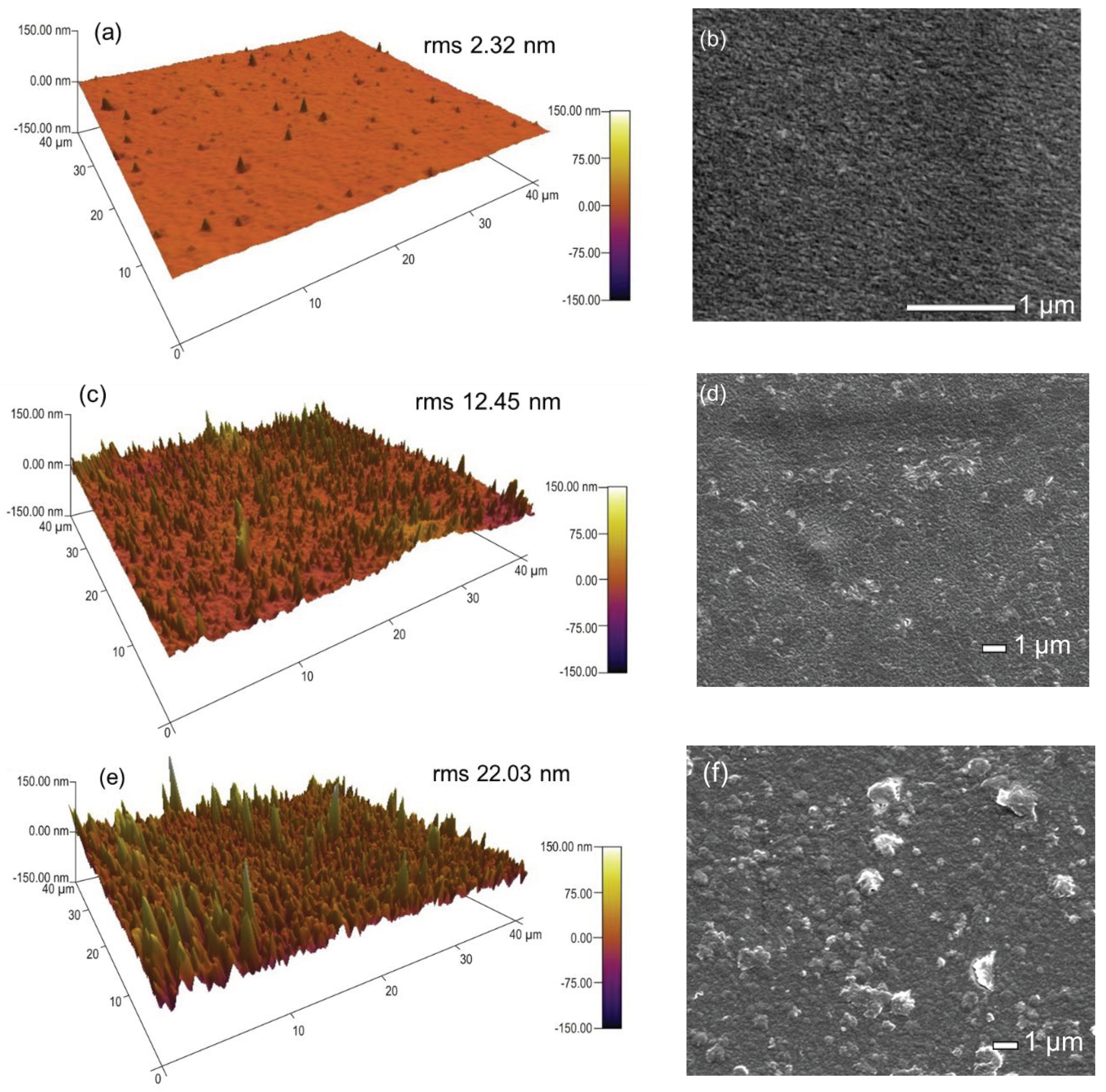
3.1.1. Structural Analysis

The surface morphologies of the samples were analyzed by using the AFM method with a scanning area of 40 × 40 μm2, as well as SEM. AFM and SEM images for the surface morphologies of AZO films on glass and PET (before and after bending) are shown in Figure 1a–f. The surface of the films on glass was reasonably smooth, with a roughness of < 3 nm. Grain growth was dense with highly homogenous distribution, as clearly seen in the 3-D AFM image of the surface. It is well known that the grain size, the distribution and the surface roughness are influenced by the sample thickness [16]. The measured root mean square (RMS) roughness of AZO/glass was about 2.3 nm. As seen from the SEM, the as-grown AZO films on both substrates–glass and PET are relatively smooth, with a uniform distribution of slightly elongated grains. The average grain size of AZO films is approximately the same, around 20 nm. The RMS roughness of AZO/PET and SEM morphology before and after bending are discussed in Section 3.1.4.

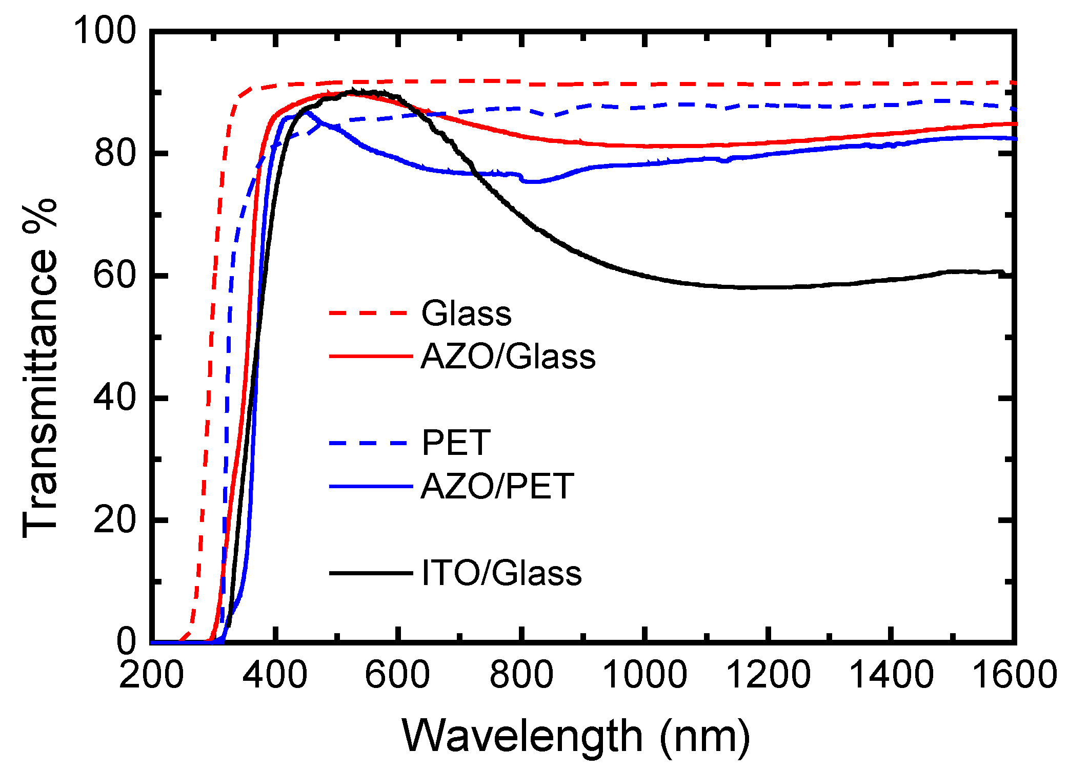
3.1.2. Optical Properties

The optical transmittance spectra of AZO films deposited on glass and PET are shown in Figure 2. The spectra of glass and PET blank substrates are also included for reference as well as commercially available ITO/glass substrate. As seen in comparison to the blank PET substrate, the absorption edges of AZO films on glass and PET are shifted to the longer wavelengths and follow a similar transmittance behavior (around 80% transmittance in visible and near-infrared regions).

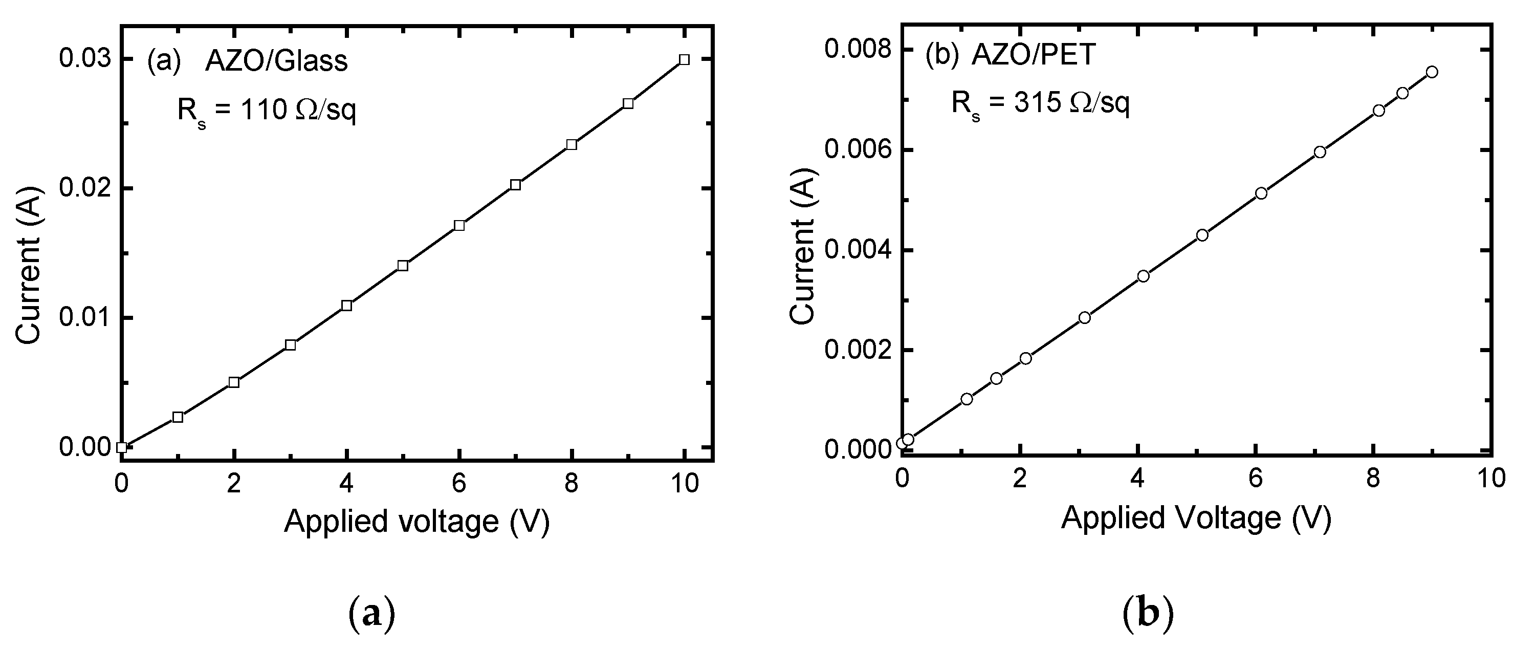
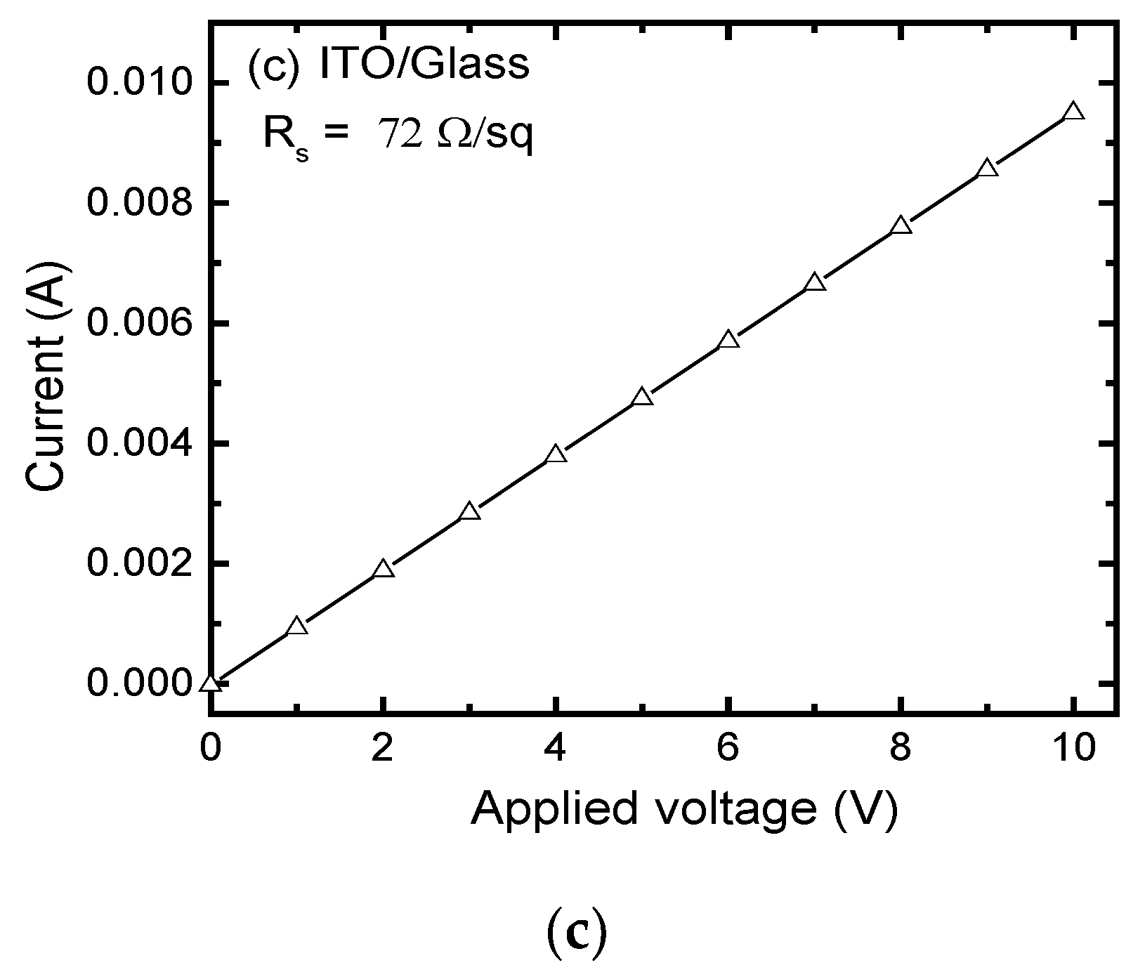
3.1.3. Electrical Properties

Next, the electrical properties were assessed. Room temperature currents versus voltage (I–V) characteristics of AZO thin films on glass and PET as well as ITO/glass are shown in Figure 3a–c. All performed current–voltage measurements show Ohmic behavior. As a device-relevant parameter, sheet resistance (Rs) = 1/σd, where σ is the electrical conductivity of the material and d is the thickness of the electrode, is used for a comparison of the transparent electrodes rather than conductivity, which is an intrinsic material property. The calculated sheet resistances are also shown in the figures.

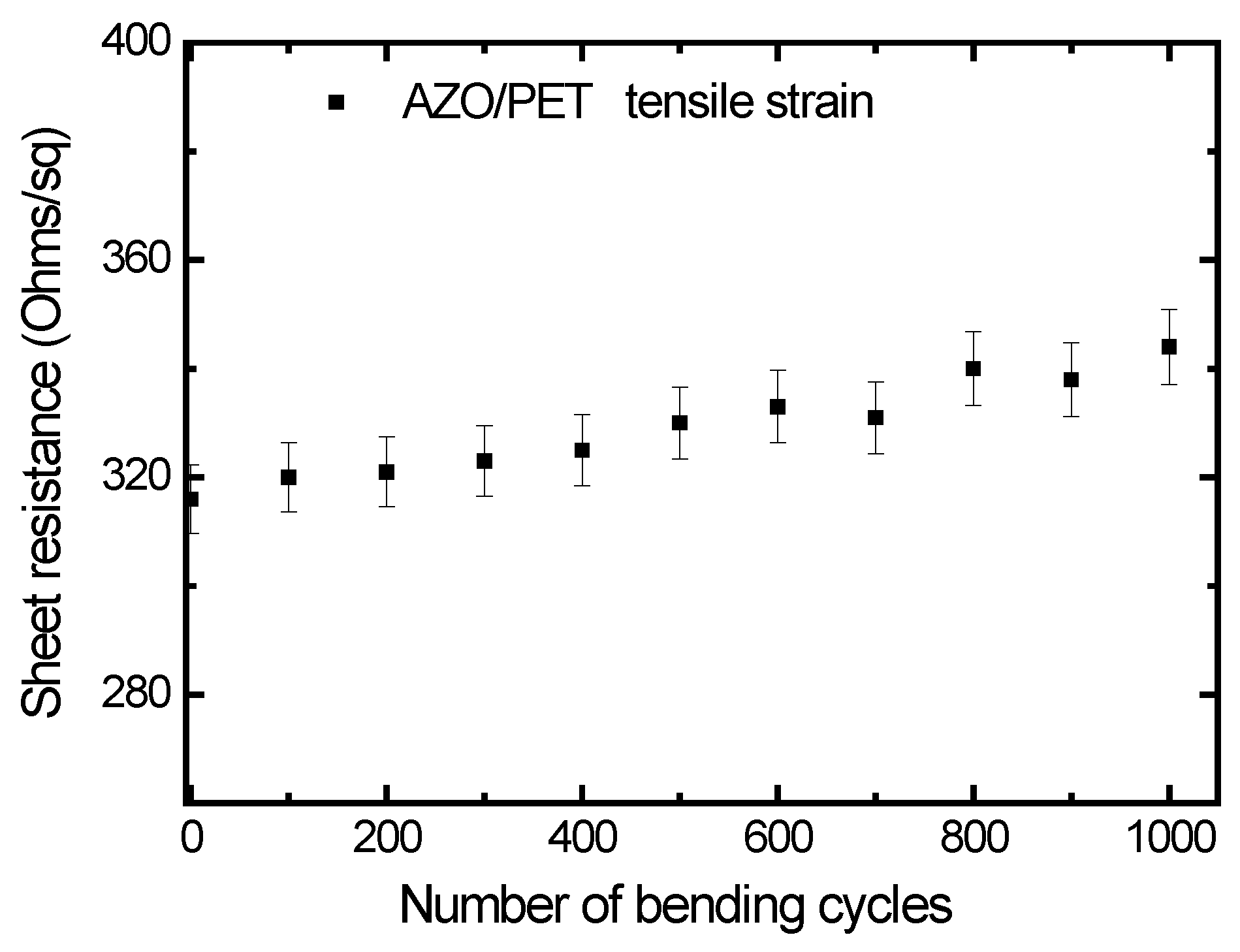
3.1.4. Bending Ability Test of AZO/PET Flexible Substrates

The bending ability test has been checked for flexible AZO/PET substrates under tensile strain. Generally, the sheet resistance (Rs) value depends on the film composition, morphology, thickness and the substrate material. After continuous bending up to 1000 times (radius of 10 mm), the sheet resistance of AZO/PET increased only slightly (see Figure 4). The RMS roughness of blank PET substrate was 6.26 nm. AZO/PET RMS was measured to be around 12 nm and it is increasing to 22 nm after 1000 bending cycles. During the bending cycles, damage in the AZO/PET develops, most probably in the form of extended defects that collapse as micro-cracks (as evidenced by SEM image in Figure 1f), capable of interrupting electrical paths on subsequent bending. Bending in–out cycles open and close these micro-cracks, and with the accumulation of the bending cycles an effective breaking of a slightly increasing number of conductive paths occurred, thus influencing the measured resistance and appearing as increased sheet resistance. These results are confirmed further by the increased roughness shown in the AFM image of the same layer, performed after 1000 bending cycles (Figure 1c).

3.2. Applications of AZO Transparent Conductive Layer for Display Applications

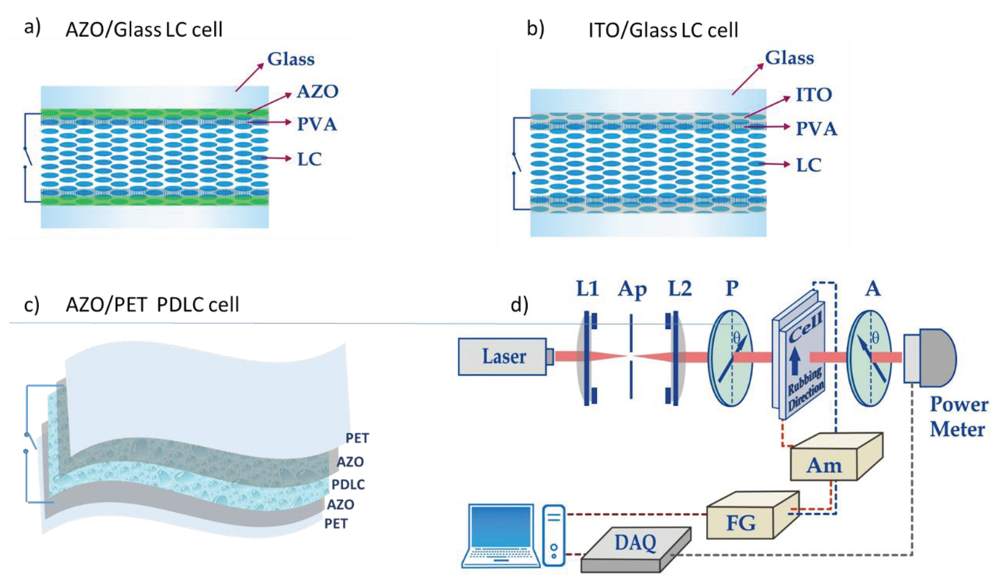
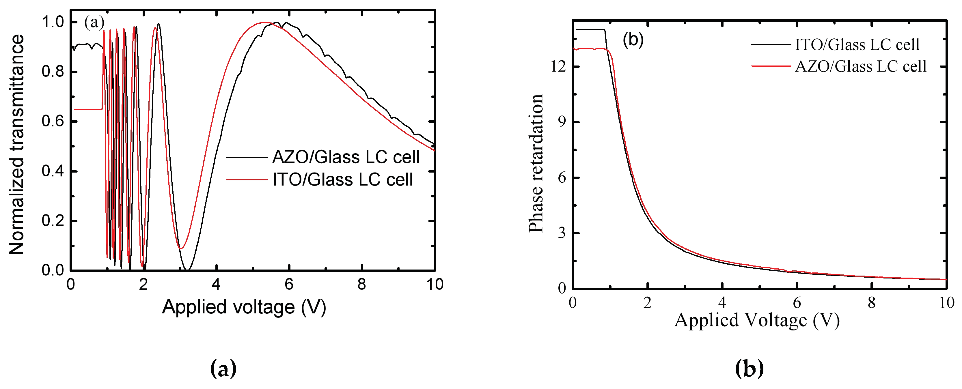
3.2.1. AZO as Transparent Conductive Layer in Rigid LC Display

Several AZO/glass samples were selected for transparent electrodes in the LC cell assembly, hereafter called an AZO-based LC rigid display. First, a Polyvinyl Alcohol (PVA) layer was spin-coated, baked at 90 °C for 30 min and post baked at 120 °C for 30 min on AZO/glass samples. Next, the PVA-coated AZO/glass substrates were mechanically rubbed for LC molecule alignment. We used nematic LC (NLC type E7, Merck, Kenilworth, NJ, USA). The cell was arranged by gluing the two rubbed layers in an anti-parallel configuration with the alignment directions facing each other. A 12-μm Mylar spacer was used to keep the same thicknesses in the fabricated cells. The liquid crystal was injected via the capillary method into the empty cell. Finally, the arranged cell was sealed with ultraviolet (UV) glue and exposed with UV light to stabilize it. Copper tape wires were used for electrical connections (see Figure 5a,b). In addition, a reference LC cell using ITO/glass was prepared following the same fabrication procedure and thickness for comparison.
For electro-optical modulation characteristic measurements, the LC cells were placed between a pair of crossed polarizers. The incident beam was polarized at the angle of 45° with respect to the nematic director (a dimensionless unit vector n, which represents the direction of the preferred orientation of LC molecules). An alternating voltage (f = 1 kHz) with varying amplitude was applied across to the LC cell to orient the LC director. A helium–neon laser (He–Ne) emitting λ = 633 nm was used to probe the changes in the transmitted intensity of LC devices under different amplitudes of driving voltage. The power of the transmitted beam was monitored by a power meter. The light transmission was measured as a function of the applied root mean square (RMS) alternating current (AC) voltage with a 1-kHz frequency. The transmittance changes were detected by positioning a photodetector behind the device (Figure 5d).
The basic operation principles of LC displays rely on the electro-optically controlled birefringence of the LC molecules [24,25]. Upon application of an electric field, since the LC molecules have a different polarizability along their long and short axis, an induced dipole moment arises and all the molecules start to reorient towards the direction of the applied field. Because of the LC’s anisotropy, the nematic LC layer acts as the birefringent material, characterized by different refractive indices for a beam polarized along the long or short molecular axis.
Figure 6a,b shows the transmitted light intensity dependence of the applied voltage for an LC cell using AZO as transparent electrode. A reference cell, assembled using a commercial ITO electrode is shown for comparison. The transmittance–voltage behavior follows the typical sinusoidal function of the amplitude of applied voltage, governed by the electrical response of the liquid crystal molecules, as expressed by [25].
T = 1 2 sin 2 Γ 2 = 1 / 2 sin 2 [ π d ( n e n 0 ) λ ]
where Γ = 2 π λ ( n e n 0 ) d is the phase retardation due to the birefringence ∆n (∆n = nen0) modulation, λ—the wavelength, d—the thickness of the LC layer and ne and n0 are the refractive indices for extraordinary and ordinary waves, respectively.
As shown in Figure 6a, the transmitted intensity follows a series of maxima and minima (so-called Fréedericksz transition), which correspond to the phase retardation, as presented in Figure 6b.
The low sheet resistance of the AZO layer has a large impact on the modulation characteristics of assembled LC cells. As seen from Figure 6a, the modulation behavior of the LC cell using AZO contacts is very similar and competitive with the LC cell using ITO. The results are also supported by the calculated Haacke figure of merit (FOM) factor of performance, expressed by the ratio between the optical transmittance (Tav) and the sheet resistance (Rs) values [26]:
FOM = T a v 10 R s
Using the transmittance data (Figure 2) and measured sheet resistance values of AZO/glass, we obtained FOM (AZO) = 1.05 × 10⁻³−1. Similar values have been calculated for (commercially available) ITO/glass, FOM (ITO) = 2.52 × 10⁻³−1. These values are in good confirmation with those previously reported [27,28] and demonstrate the high potential of AZO films as transparent electrodes for ITO-free LCD devices (Table 1).

3.2.2. AZO as Transparent Conductive Layer in Flexible Display (Smart Structures)

PDLC-based structures have attracted increasing attention for applications as outdoor displays, switchable privacy glasses, energy saving windows, light shutters, projection displays, and so on [29,30]. Here, the PDLC film was prepared using a polymerization-induced phase separation method, based on the phase separation of the LC (E7, Merck, n0 = 1.521 and ne = 1.72) and photo-curable adhesive polymer matrix (NOA65, Norland, Cranbury, NJ, USA, n = 1.524) with a 3:7 weight ratio. During the fabrication of our flexible PDLC structures, supported by AZO/PET substrates, we perform the following steps: first, an empty cell was prepared by gluing two AZO/PET substrates with 12-μm Mylar spacers between them. Then, the LC/monomer mixture was injected into the empty cell and, finally, the cell was exposed with ultraviolet light ((λ = 365 nm) with an intensity of 60 mW/cm2 for 15 min) to polymerize NOA65. As a result, using the polymerization-induced phase separation method, randomly dispersed liquid crystal droplets (usually in micrometer size) are formed within a transparent polymer matrix. Figure 5c shows the schematic structure of the AZO/PET PDLC flexible device.

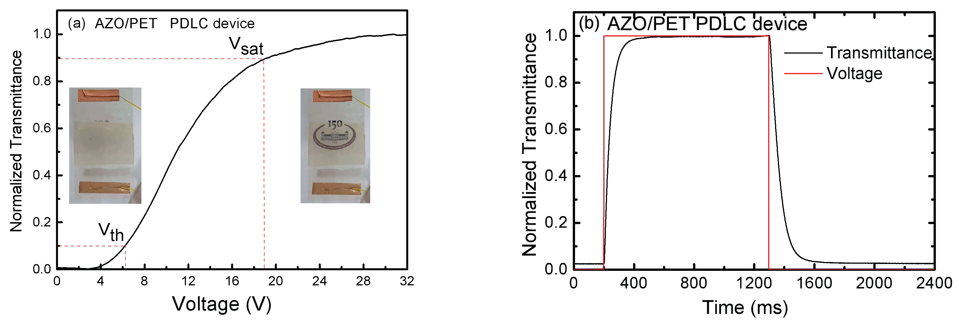
3.2.3. Electro-Optical Characteristics and Bending Test Ability

In general, PDLC can be switched between a light-scattering to a transparent state by applying an external electric field. The effect results from a mismatch or match of refractive indices between the LC molecules and the polymer matrix and is due to the LC birefringence and the ability of an applied voltage to re-orient the LC molecules inside the droplets in order to match the LC’s refractive index to that of the polymer matrix. The electro-optical characteristics were measured by an optical setup, shown in Figure 5d. In these measurements, the polarizer and analyzer were removed from the setup, since the polymer defines the polarization state of the PDLC film.
The typical transmittance dependence of the assembled AZO/PET PDLC device as a function of the applied voltage is shown in Figure 7a. Without an applied voltage, the LC molecules are randomly oriented in the droplets, which causes light scattering when the light passes through the structure. As a result, the “scattering” state appears. When the voltage is applied, the electric field aligns the LC’s nematic director to the direction of the electric field, allowing light to pass through the droplets. As a result, a “transparent” state appears. Thus, the intensity of the transmitted light through the PDLC structure can be controlled by the application of an external voltage.
For the AZO/PET device shown in Figure 7a, we defined (i) the threshold voltage Vth as a value of the applied voltage necessary to reach 10% of the maximum transmittance, e.g., to “turn on” the PDLC cell (measured Vth ~ 6.1 V) and (ii) the saturation voltage Vsat, defined as the value of applied voltage required to reach 90% of maximum transmittance T (Vsat ~18 V). As seen, at the saturation state, the PDLC structure becomes transparent (the “BAS LOGO” image pattern become clear).
In addition, the response time of the assembled PDLC device for switching between “off“ and “on“ states was measured and is presented in Figure 7b. The measured response time and the fall time values were ~68 and ~88 ms, respectively. These values are very similar to the reported values for PDLC devices using other transparent contacts [31,32].
To sum up, the implementation of AZO layers as transparent conductive electrodes in LC and PDLC devices requires the synthesis of high uniformity, conformal and compact layers by an appropriate process such as ALD. The AZO films obtained by ALD technique enable low sheet resistance and high optical transparency through the use as transparent electrodes on the top surfaces of both the selected rigid and flexible substrates.

4. Conclusions

In summary, we studied the structural and optical properties and the sheet resistance ability of AZO layers deposited by the ALD technique onto glass and PET substrates. LC devices with transparent AZO electrodes were successfully fabricated, and the measured driving voltage and response time values show the great potential of AZO for integration as functional transparent conducting material. We expect that the above demonstrations will be relevant for further applications in high-end optoelectronics.

Author Contributions

Conceptualization, V.M., S.H.L., and K.Y.H.; methodology D.D., B.B., S.P., and D.P.; software, S.P., C.-L.T., V.S., and B.N.; formal analysis, V.M., S.H.L., and K.Y.H.; resources D.D., V.M., and S.H.L.; writing—original draft preparation, D.D., and V.M.; writing—review and editing D.D., C.-L.T., V.M., B.B., S.P., D.P., V.S., B.N., S.H.L., and K.Y.H.; visualization, D.D., C.-L.T., V.M., S.P., D.P. and V.S.; supervision, V.M., S.H.L., and K.Y.H.; funding acquisition D.D., V.M., and S.H.L. All authors have read and agreed to the published version of the manuscript.

Funding

This research was funded by the Bulgarian Science Fund under the Grant No. K∏-06-H-28/8 and the Ministry of Science and Technology (MOST), Taiwan, under the Grant No.: MOST 107-2221-E-009-120-MY3 and MOST 109-2927-I-009-507. We are grateful for the support from the Higher Education Sprout Project of the National Chiao Tung University and Ministry of Education (MOE), Hsinchu, Taiwan. Research equipment from the distributed research infrastructure INFRAMAT (part of the Bulgarian National roadmap for research infrastructures), supported by the Bulgarian Ministry of Education and Science under contract D01-284/17.12.2019, was used for AFM measurements.

Acknowledgments

The authors would like to thank P. Terziyska from the ISSP, BAS, Bulgaria for determining the AZO layer’s thickness and to Marina Vasileva from the IOMT, BAS, Bulgaria for the measurement of the optical spectra. The authors gratefully acknowledge the financial support provided by the Bulgarian Science Fund under the grant number K∏-06-H-28/8 and the Ministry of Science and Technology (MOST), Taiwan, under the grant numbers MOST 107-2221-E-009-120-MY3 and MOST 109-2927-I-009-507 (Bulgarian–Taiwanese PPP exchange program). We are grateful for the support from the Higher Education Sprout Project of the National Chiao Tung University and Ministry of Education (MOE), Taiwan. Research equipment from the distributed research infrastructure INFRAMAT (part of the Bulgarian National roadmap for research infrastructures), supported by the Bulgarian Ministry of Education and Science under contract D01-284/17.12.2019, was used for AFM measurements.

Conflicts of Interest

The authors declare no conflict of interest.

References

  1. Ellmer, K. Past achievements and future challenges in the development of optically transparent electrodes. Nat. Photonics 2012, 6, 809–817. [Google Scholar] [CrossRef]
  2. Gordon, R.G. Criteria for choosing transparent conductors. MRS Bull. 2000, 25, 52–57. [Google Scholar] [CrossRef] [Green Version]
  3. Morales-Masis, M.; De Wolf, S.; Woods-Robinson, R.; Ager, J.W.; Ballif, C. Transparent electrodes for efficient optoelectronics. Adv. Electron. Mater. 2016, 3, 1600529. [Google Scholar] [CrossRef] [Green Version]
  4. Levy, D.; Castellon, E. Transparent Conductive Materials: Materials, Synthesis, Characterization, Applications, 1st ed.; Wiley-VCH Verlag Gmbh &Co, KGaA: Weinheim, Germany, 2018. [Google Scholar]
  5. Transparent Conductive Films Market by Application (Smartphones, Tablets, Notebooks, LCDs, Wearable Devices), Material (ITO on Glass, ITO on PET, Metal Mesh, Silver Nanowires, Carbon Nanotubes), and Region-Global Forecast to 2026. Available online: https://www.marketsandmarkets.com/Market-Reports/transparent-conductive-film-market-59909084.html (accessed on 30 April 2020).
  6. Suzuki, A.; Matsushita, T.; Wada, N.; Sakamoto, Y.; Okuda, M. Transparent conducting Al-doped ZnO thin films prepared by pulsed laser deposition. Jpn. J. Appl. Phys. 1996, 35, L56–L59. [Google Scholar] [CrossRef]
  7. Berginski, M.; Hupkes, J.; Schulte, M.; Schope, G.; Stiebig, H.; Rech, B.; Wuttig, M. The effect of front ZnO:Al surface texture and optical transparency on efficient light trapping in silicon thin-film solar cells. J. Appl. Phys. 2007, 101, 074903. [Google Scholar] [CrossRef]
  8. Minami, T.; Sato, H.; Nanto, H.; Takata, S. Heat treatment in hydrogen gas and plasma for transparent conducting oxide films such as ZnO, SnO2 and indium tin oxide. Thin Solid Films 1989, 176, 277–282. [Google Scholar] [CrossRef]
  9. Dhere, R.G.; Bonnet-Eymard, M.; Charlet, E.; Peter, E.; Duenow, J.N.; Li, J.V.; Kuciauskas, D.; Gessert, T.A. CdTe solar cell with industrial Al:ZnO on soda-lime glass. Thin Solid Films 2011, 519, 7142–7145. [Google Scholar] [CrossRef]
  10. Vasekar, P.S.; Dhere, N.G.; Moutinho, H. Development of CIGS2 solar cells with lower absorber thickness. Sol. Energy 2009, 83, 1566–1570. [Google Scholar] [CrossRef]
  11. Park, S.; Ikegami, T.; Ebihara, K. Growth of transparent conductive Al-doped ZnO thin films and device applications. Jpn. J. Appl. Phys. 2006, 45, 8453–8456. [Google Scholar] [CrossRef]
  12. Verma, A.; Khan, F.; Kumar, D.; Kar, M.; Chakravarty, B.C.; Singh, S.N.; Husain, M. Sol–gel derived aluminum doped zinc oxide for application as anti-reflection coating in terrestrial silicon solar cells. Thin Solid Films 2010, 518, 2649–2653. [Google Scholar] [CrossRef]
  13. Mondragon-Suarez, H.; Maldonado, A.; de la L Olvera, M.; Reyes, A.; Castanedo-Perez, R.; Torres-Delgado, G.; Asomoza, R. ZnO:Al thin films obtained by chemical spray: Effect of the Al concentration. Appl. Surf. Sci. 2002, 193, 52–59. [Google Scholar] [CrossRef]
  14. Ma, J.; Ji, F.; Ma, H.; Li, S. Preparation and properties of transparent conducting zinc oxide and aluminium-doped zinc oxide films prepared by evaporating method. Sol. Energy Mater. Sol. Cells 2000, 60, 341–348. [Google Scholar] [CrossRef]
  15. Liu, Y.; Lian, J. Optical and electrical properties of aluminum doped ZnO thin films grown by pulsed laser deposition. Appl. Surf. Sci. 2007, 253, 3727–3730. [Google Scholar] [CrossRef]
  16. Yang, W.; Wu, Z.; Liu, Z.; Pang, A.; Tu, Y.; Feng, Z.C. Room temperature deposition of Al-doped ZnO films on quartz substrates by radio-frequency magnetron sputtering and effects of thermal annealing. Thin Solid Films 2010, 519, 31–36. [Google Scholar] [CrossRef]
  17. Kon, M.; Song, P.K.; Shigesato, Y.; Frach, P.; Mizukami, A.; Suzuki, K. Al-doped ZnO films deposited by reactive magnetron sputtering in mid-frequency mode with dual cathodes. Jpn. J. Appl. Phys. 2002, 41, 814–819. [Google Scholar] [CrossRef]
  18. Tynell, T.; Yamauchi, H.; Karppinen, M.; Okazaki, R.; Terasaki, I. Atomic layer deposition of Al-doped ZnO thin films. J. Vac. Sci. Technol. A 2013, 31, 01A109. [Google Scholar] [CrossRef] [Green Version]
  19. Johnson, R.W.; Hultqvist, A.; Bent, S.F. A brief review of atomic layer deposition: From fundamentals to applications. Mater. Today 2014, 17, 236–246. [Google Scholar] [CrossRef]
  20. Dhakal, T.; Nandur, A.S.; Christian, R.; Vasekar, P.; Desu, S.; Westgate, C.; Koukis, D.I.; Arenas, D.J.; Tanner, D.B. Transmittance from visible to mid infra-red in AZO films grown by atomic layer deposition system. Sol. Energy 2012, 86, 1306–1312. [Google Scholar] [CrossRef]
  21. Tulzo, H.L.; Schneider, N.; Lincot, D.; Patriarche, G.; Donsanti, F. Impact of the sequence of precursor introduction on the growth and properties of atomic layer deposited Al-doped ZnO films. J. Vac. Sci. Technol. A 2018, 36, 041502. [Google Scholar] [CrossRef] [Green Version]
  22. Blagoev, B.S.; Dimitrov, D.Z.; Mehandzhiev, V.B.; Kovacheva, D.; Terziyska, P.; Pavlic, J.; Lovchinov, K.; Mateev, E.; Leclercq, J.; Sveshtarov, P. Electron transport in Al-doped ZnO nanolayers obtained by atomic layer deposition. J. Phys. Conf. Ser. 2016, 700, 012040. [Google Scholar] [CrossRef]
  23. Sweet, W.J., III; Jur, J.S.; Parsons, G.N. Bi-layer Al2O3/ZnO atomic layer deposition for controllable conductive coatings on polypropylene nonwoven fiber mats. J. Appl. Phys. 2013, 113, 194303. [Google Scholar] [CrossRef]
  24. Yeh, P.; Gu, C. Optics of Liquid Crystal Display; Wiley Interscience: New York, NY, USA, 2010. [Google Scholar]
  25. Khoo, I.C. Liquid Crystals Physical Properties and Nonlinear Optical Phenomena; Wiley: Hoboken, NJ, USA, 1995. [Google Scholar]
  26. Haacke, G. New figure of merit for transparent conductors. J. Appl. Phys. 1976, 47, 4086–4089. [Google Scholar] [CrossRef]
  27. Oh, B.-Y.; Jeong, M.-C.; Moon, T.-H.; Lee, W.; Myoung, J.-M.; Hwang, J.-Y.; Seo, D.-S. Transparent conductive Al-doped ZnO films for liquid crystal displays. J. Appl. Phys. 2006, 99, 124505. [Google Scholar] [CrossRef]
  28. Su, Y.C.; Chiou, C.C.; Marinova, V.; Lin, S.H.; Bozhinov, N.; Blagoev, B.; Babeva, T.; Hsu, K.Y.; Dimitrov, D.Z. Atomic layer deposition prepared Al-doped ZnO for liquid crystal displays applications. Opt. Quantum Electron. 2018, 50, 205. [Google Scholar] [CrossRef]
  29. Baetens, R.; Jelle, B.P.; Gustavsen, A. Properties, requirements and possibilities of smart windows for dynamic daylight and solar energy control in buildings: State-of-the-art. Sol. Energy Mater. Sol. Cells 2010, 94, 8–105. [Google Scholar] [CrossRef] [Green Version]
  30. Chung, S.H.; Noh, H.Y. Polymer-dispersed liquid crystal devices with graphene electrodes. Opt. Express 2015, 23, 32149. [Google Scholar] [CrossRef]
  31. Sannicolo, T.; Lagrange, M.; Cabos, A.; Celle, C.; Simonato, J.P.; Bellet, D. Metallic Nanowire-based transparent electrodes for next generation flexible devices: A review. Small 2016, 12, 6052–6075. [Google Scholar] [CrossRef]
  32. Huang, Q.; Shen, W.; Fang, X.Z.; Chen, G.; Yang, Y.; Huang, J.; Tan, R.; Song, W. Highly thermostable, flexible, transparent, and conductive films on polyimide substrate with an AZO/AgNW/AZO structure. ACS Appl. Mater. Interfaces 2015, 7, 4299–4305. [Google Scholar] [CrossRef]
Figure 1. Atomic Force Microscopy (AFM) and SEM analysis of aluminum-doped zinc oxide (AZO) layers deposited on (a,b) AZO/glass (c,d) AZO/polyethylene terephthalate (PET) (before bending test) and (e,f) AZO/PET (after bending 1000 times, discussed in 3.1.4.).
Coatings 10 00539 g001
Figure 2. Transmittance spectra of AZO/glass and AZO/PET. Blank glass and PET spectra are also shown for reference, as well as commercial indium tin oxide (ITO)/glass.
Coatings 10 00539 g002
Figure 3. Current–voltage characteristics of AZO thin films deposited on (a) glass and (b) PET, as well a comparison with (c) commercial ITO/glass, are shown for reference.
Coatings 10 00539 g003aCoatings 10 00539 g003b
Figure 4. Sheet resistance dependence of the number of bending cycles for AZO layer on PET substrate.
Coatings 10 00539 g004
Figure 5. Schematic diagrams of: (a) AZO/glass LC cell; (b) ITO/glass LC cell and (c) AZO/PET polymer-dispersed liquid crystal (PDLC) cell and (d) experimental setup to measure the electro-optical modulation behavior. Legend: lens (L), aperture (Ap), polarizer (P), analyzer (A), amplifier (Am), function generator (FG), data acquisition card (DAQ). Note: for PDLC cell measurements, the P and A are removed from the setup.
Coatings 10 00539 g005
Figure 6. (a) Transmittance–voltage characteristics of AZO/glass and ITO/glass (reference) LC cells and (b) phase retardation for both LC cells.
Coatings 10 00539 g006
Figure 7. (a) Voltage-transmittance behavior of AZO/PET PDLC device and (b) the response time.
Coatings 10 00539 g007
Table 1. Haacke figures of merit (FOM).
LC Cell TypeTav (%)Rs (Ω/sq)FOM (Ω−1)
AZO/Glass80.61101.05 × 10−3
ITO/Glass84.3722.52 × 10−3

