Review

Ultra-Short Pulsed Laser Deposition of Oxides, Borides and Carbides of Transition Elements

Dipartimento di Scienze, Università della Basilicata, Via Ateneo Lucano 10, 85100 Potenza, Italy
*
Author to whom correspondence should be addressed.
Coatings 2020, 10(5), 501; https://doi.org/10.3390/coatings10050501
Submission received: 30 April 2020 / Revised: 18 May 2020 / Accepted: 21 May 2020 / Published: 23 May 2020
(This article belongs to the Special Issue Surface Function Enhancement Film and Coating Technology)

Abstract

:
Oxides, borides and carbides of the transition elements are materials of great interest from a technologic point of view. Many of these materials are used in the form of thin films, so several techniques are commonly used to deposit them. Among these techniques, Pulsed Laser Deposition (PLD) performed using ultra-short pulse lasers, mainly fs lasers, presents unique characteristics in respect to PLD performed using conventional short pulse lasers. Indeed, the films deposited using fs PLD are often nanostructured, and this technique often allows the target stoichiometry to be transferred to the films. In this work, we will review the use of ultra-short PLD in the production of films obtained from transition metal oxides, borides and carbides, evidencing the advantages offered by this technique, together with the problems arising with some of the studied systems. We conclude that even if ultra-short PLD is surely one of the most important and useful deposition techniques, it also presents limits that cannot be ignored.

1. Introduction

The binary compounds of the first elements of the groups 13 (boron), 14 (carbon) and 16 (oxygen) of the periodic table with transition elements are materials of great interest since many of these compounds find large application for their peculiar characteristics. For example, titanium carbide, due to its high thermal stability and good resistance against corrosion, is largely used as refractory material [1], while titanium diboride, in addition to similar physical-chemical properties, presents strong electrical conductivity, higher than that of pure titanium [2], and a very high microhardness [3]. Borides, carbides and oxides can be generally classified, from the point of view of electric conductivity, as dielectrics but some of these compounds, for example zinc oxide, are semiconductors, while others, for example the already cited titanium diboride, are excellent electrical conductors, evidencing once again the large spectrum of their possible applications. Many of these compounds can be used as bulk materials, but a large number are also utilized in the form of thin films for improving the performances of bulk materials.
In general, a film is considered thin if it has a thickness between a few nanometers and 10 micrometers, but most thin films present a thickness of the order of 1 μm or less. The deposition of thin films on the surface of a bulk material with different composition is a method widely used to modify some of the material characteristics. Typical examples are the anticorrosion coatings on metal alloys or those films improving the tribological properties of machine elements and cutting tools [4], but thin films can also be used as optical layers [5] or exchange membrane in fuel cells [6].
Many different techniques can be used to obtain thin films of materials with technological interest [7,8], but surely one of the most interesting is based on laser ablation. In fact, laser ablation has proved to be a versatile and powerful method for the preparation of a great variety of materials. Even though continuous wave lasers can be used to ablate solid targets, laser ablation is in general performed using pulsed lasers and in this case is currently known as Pulsed Laser Ablation (PLA). This method has been shown to be suitable not only to deposit thin films, often maintaining the stoichiometry and properties of bulk targets, but also in order to obtain products with peculiar properties which in some cases are quite different from those of the starting material [9,10]. In addition, this technique is particularly suited for the preparation of nanostructured films and, in general, can enable the growth of nanostructures (nanorods, nanoneedles) on the substate surface [11,12,13].
The interaction between the laser radiation and the target produces a material removal (ablation), originating a plasma, often called plume for its particular shape, the characteristics of which (temperature, density, velocity, composition and shape) depend on laser and target parameters and on the medium whereby its expansion takes place. The materials forming the plasma can be deposited on a substrate placed in a suitable position to produce the growth of a thin film. This technique is called Pulsed Laser Deposition (PLD) and can be carried out both in vacuum and in the presence of an inert or reactive buffer gas. The experimental set-up for PLD experiments in vacuum and in the presence of a buffer gas is often very simple, and this is one of the reasons for the success of this technique from an applicative point of view [10].
The scheme of typical experimental apparatus is reported in Figure 1, and basically, it consists of a laser source, a vacuum chamber equipped with a target holder, a gas inlet to fill the chamber with a buffer gas and a substrate holder, often heatable, in a suitable position. In general, the laser beam impinges on the target with an angle of 45°, and the substrate is positioned in front of the target, but the geometry of the system can be varied to allow the performing of different diagnostic methods or for particular purposes. The use of shadow masks makes it possible to adjust the effect of particles ejected from the target on the performance of the coatings [14]. The application of pulsed electric fields during the expansion of the laser-initiated plasma causes the high-energy ion implantation and the ion mixing of materials at the film-substrate interface [15]. Anyway, the majority of the PLD experiments reported in literature have been carried out with an experimental apparatus of the type shown in Figure 1.
Given that oxides, borides and carbides of transition elements, in the form of thin films, are of great interest from a technologic point of view and that ultra-short PLD is one of the most useful methods for thin film preparation, this review will present an overview of the state of the art in the application of ultra-short PLD to the above cited systems. The last review on fs ablation of dielectrics and its applications for thin film deposition was published in 2013 by Balling and Schou [16], but it was mainly devoted to the dynamics of the ablation process and referred to a very large class of compounds.
Finally, in general, ultra-short PLD is carried out by using lasers with pulse durations in the range of fs, so even if some cases of the use of ps lasers are reported, in this review ultra-short pulse laser will often be a synonym of fs laser and vice versa.
Considering the importance of plasma characteristics for PLD, in the following section a brief description of the principles of PLA will be reported, with particular attention to the expansion of the plasma in vacuum since a large part of the systems reviewed in this work were deposited in those conditions.

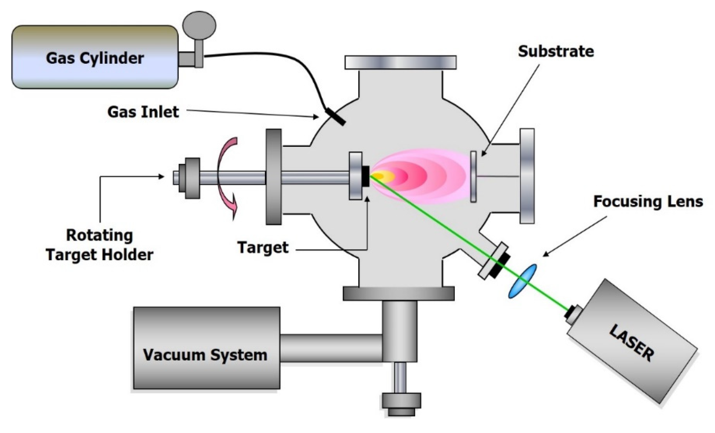
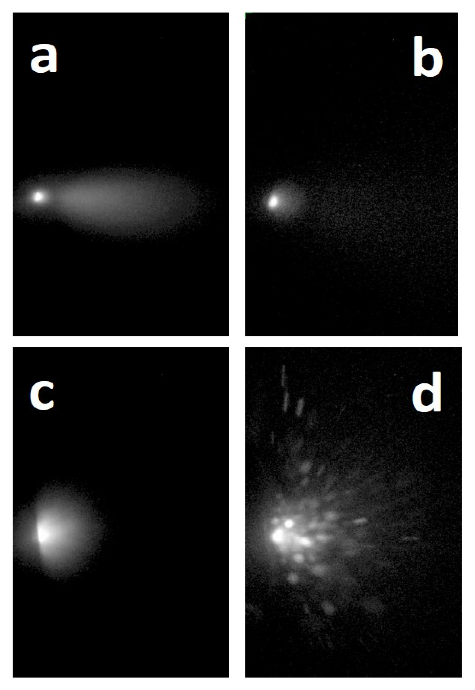
2. Ultra-Short Pulsed Laser Ablation

As already mentioned, pulsed laser ablation is the expression currently used to describe the explosive vaporization which occurs when a high-peak power laser beam is focused onto a solid or, less commonly, a liquid. The interaction of the laser beam with the target produces the ejection of atoms, ions, electrons, molecules, clusters and, in some cases, particles with different dimensions. All these components make up a plasma, characteristic of the PLA process. The energy required to produce such a plasma depends both on the characteristics of the target material and on the laser wavelength and pulse duration. The plasma expands three-dimensionally, with a very high (102–107 cm s−1) velocity depending on the type of travelling particles and on the wavelength, power and time duration of the ablation laser pulse, as well as on the employed background characteristics [17]. Indeed, the presence of a buffer gas in the ablation chamber can drastically change the expansion conditions for the plasma. The addition of a buffer gas produces two effects on the expanding plasma. First of all, the collisions with the gas particles, which often, but not necessarily, present a large mass, produce a decrease of the kinetic energy of the plasma components. On the other hand, the presence of the surrounding gas leads to the confinement of the plasma in a smaller volume with respect to free expansion into the vacuum [18]. All these conditions favour the nucleation and growth of clusters [19,20]. Of course, the slowing down and confinement of plasma components are only two of the phenomena involved in the expansion of a laser produced plasma in an inert buffer gas, which include formation of shock waves, diffusion and scattering processes, thermalisation of the particles, etc. [21]. There are a large number of works and comprehensive books discussing the laser-matter interaction processes involved in PLA [9,10,17,19,22], therefore only a brief description of the phenomenon will be presented here.
It is evident that both the characteristics of the target and those of the laser source play a fundamental role in the laser ablation process. Considering the target, all its thermo-physical properties can influence the ablation process, even considering the fundamental difference between metals and nonmetallic solids. On the other hand, even if the laser wavelength, energy and repetition rate can influence the laser-matter interaction and, as a consequence, the plasma characteristics, the pulse time duration (τ) of the laser can be considered as the most important parameter. In the regime of short (10 ps < τ < 100 ns) or ultra-short (τ < 10 ps) laser pulses, different laser–mater interaction mechanisms can occur giving origin to plasmas with different characteristics and composition. In this work we will consider only films deposited using PLD performed with ultra-short pulse lasers, so we will limit our description to the plasma generated using these types of laser.
Ultra-short pulse lasers are now currently used in many scientific and industrial fields, and the development of these laser sources, carried out from the beginning of the nineties, has been reported in some review papers by Ursula Keller [23,24]. Today the evolution of these lasers is far from being concluded, especially regarding the sources with very high repetition rates, up to gigahertz [25,26]. These high repetition rate fs laser sources are especially used in materials and surface processing, but they find application also in PLD. Indeed, even if the repetition rates useful for PLD cannot exceed some kHz, these high values can strongly increase the deposition rates of the films, filling the gap with the performances of PLD carried out using ns lasers [16].
The mechanisms and dynamics of PLA carried out using fs lasers have been exhaustively treated in the review of Balling and Schou on the fs laser ablation of dielectrics and semiconductors [16], so in this paper we only report a brief summary of the characteristics of the plasma produced using ultra-short PLA, in relation to the morphology and composition of the deposited films.
When the plasma produced in vacuum by ultra-short PLA was analyzed using Optical Emission Spectroscopy (OES), two different emissions of material, occurring at very distinctive time delays in respect to the laser pulse and with different composition and velocity were detected by Albert and co-workers [27]. During the first microsecond a luminous plasma developed, the so-called primary plume, whose spectrum presented emission lines corresponding to atoms and small molecules. When the luminescence of this plasma component was quenched, a second material emission took place. The peculiar feature of this secondary plume was related to its blackbody-like emission, which, depending on the type of material, could last up to several tens of microseconds [27]. From the spectra it was evident that the primary plume gaseous phase was formed by neutral and ionized atoms, molecules and small clusters. In contrast, as evidenced by the blackbody-like continuum emission spectrum, the secondary component was formed of particles or large clusters [27,28,29]. The velocity of these two plumes was very different. In the case of the primary plume, the front velocity was of the order of 106–107 cm/s, whereas the value was ~104 cm/s in the case of the secondary one. In addition, in some cases, a third emission of material in the form of microparticles was detected [30,31,32] (Figure 2). What is the reason for these different emissions of material?
When an ultra-short pulse interacts with a material, the laser energy is deposited very rapidly into the target, and since the laser pulse length is shorter than the time needed to couple the electronic energy to the lattice (few ps) while the thermal equilibrium of the electrons requires even shorter times (from hundred fs to few ps), a hot electron gas not in equilibrium with the lattice is generated. In addition, the electron-lattice coupling is faster than the thermal diffusion. The layers near the material surface are heated very rapidly, reaching a very high temperature, and consequently, a vaporization process producing a plasma containing electrons, atoms and small molecules is induced. This emission of material is not the only phenomenon taking place. In fact, according to molecular dynamic and hydrodynamic simulations, the larger part of the ablated material is ejected in a second time in the form of NPs, droplets, micrometric fragments, coming from deeper layers of the ablated target [33,34,35]. Also in the case of ultra-short PLA, the characteristics of the environment influence the plasma dynamics and composition. In this respect the most important consequence is that while in vacuum the materials emitted from the target at different times expand with different velocities and so are easily separated; in a buffer gas the smallest species are slowed down due to the collision with the background. The result can be, in many cases, space overlapping of the different species, with the possibility of further interactions.
When the first films were deposited in vacuum from PLD performed using ultra-short pulse laser, their morphology appeared particular. In fact, they were apparently formed by the coalescence of a large number of spherical particles with nanometric size, as clearly evidenced by Scanning Electron Microscopy (SEM) images [27,36,37].
From both the results of plume and thin films analyses it was evident that one of the main characteristics of ultra-short PLA in vacuum was the presence in the plasma of a large number of NPs. These particles showed a quite narrow range of dimensions (1–100 nm), very different from the features displayed by ns PLA processes. These NPs seem to form the main constituents of the films deposited by ultra-short PLD in the case of many different systems, independently from the type of materials [38,39,40,41].
The origin of the particles forming the secondary plume is still a matter of discussion. In general, also considering the absence of large clusters in ultra-short PLA plasmas [42], there is growing agreement about the possibility of their direct ejection from the target [16,39,40,43,44]. In this case it can be confirmed that the ablation mechanism should involve the emission of both gaseous material and melted particles.
The presence of different steps of material emission (mainly primary and secondary plumes) clearly influences the distribution and thickness of the deposits. Trelenberg et al. found that the films deposited using fs PLD presented an angular distribution corresponding to a sum of two cosines, with different exponents, for both metal alloys and semiconductors [45,46]. For example, for GaAs the thickness of the deposited material as a function of angle fitted well to a sum of two cosines, cos47θ + cos4θ [45]. The conclusion was that probably more than one ablation process was responsible for the growth of the film. Teghil et al. carried out similar measurements of the angular distribution of Al65Cu23Fe12, Al70Cu20Fe10 and Al70Pd20Mn10 films [47,48], finding a correspondence with the angular distribution of the primary and secondary plumes. For example, in the case of Al65Cu23Fe12 quasicrystal the angular distribution of the film was fitted as the combination of two different components, cos36θ + cos10θ, corresponding to angular distributions of the secondary and primary plumes respectively [47]. For this system, the film thickness varied from about 1.7 μm at the center to a few nm at the border, with a target-substrate distance of 2.5 cm and a substrate surface of 4 cm2.
From these results is evident that, in case of fs PLD, to minimize the thickness inhomogeneity of the films, operating with a large target-substrate distance is better.
In general, ultra-short PLD experiments have been performed in vacuum. Because of a large production of NPs in these conditions, a lesser number of works concerning ultra-short PLD in the presence of a buffer gas have been performed, and in particular, there are few studies about the influence of ambient gas on NP production. The works of Henley and Al-Shboul, based on OES of graphite, for instance, refer only to the dynamics of the primary plume [49,50].

3. Oxides

In this section we will look only at binary oxides, even if doped binary oxides like ITO (indium-thin oxide) will also be considered. This means that complex oxides like Yttrium-Barium-Copper Oxide (YBCO) and other high temperature superconductors will not be considered here. In general, while PLD performed using short pulse lasers has been widely used to deposit oxides (see, for ZnO, Kumar et al. [51]), up today, only a few transition metal oxides have been deposited using ultra-short PLD.

3.1. Zinc Oxide

ZnO was the first simple oxide deposited using ultra-short PLD and the reason is probably to be found in the renewed interest, in the early 2000 s, on its optoelectronic applications as a semiconductor with a direct wide band gap [52]. In 2000, Okoshi et al. deposited ZnO thin films in vacuum using PLD performed by a laser (λ = 790 nm) with a 130 fs pulse duration [53] and with E = 10 mJ. The substrates were Si (100) and quartz, and the results indicated that the films were crystalline in both cases with the best crystallinity obtained for the films deposited at a substrate temperature of 230 °C. In the same year, a paper on the same topic was published by Millon et al. [54]. In this case a laser with a pulse duration of 90 fs (λ =620 nm, E = 1 mJ) was used to grow heteroepitaxial ZnO thin films on (0001) sapphire substrates. The same group, in a paper published in 2002, compared ZnO films deposited using fs PLD with those obtained by ns PLD [55], evidencing strong differences in the films deposited by the two techniques, differences justified by the higher energies of the atomic species present in the fs plume. Okoshi et al. published a paper in 2001 comparing the results of PLD performed on a ZnO target doped with Al2O3 (2 wt % Al2O3) using lasers of different pulse durations and different wavelengths (λ = 690 nm with a pulse duration of 130 fs and λ = 395 nm with a pulse duration of 230 fs) [56]. The results evidenced a dependence on the laser wavelength of the electrical properties of the films even if their real composition was not clearly reported. A brief summary and discussion of these first works on fs PLD of ZnO was later reported by Perriere et al. in a chapter of a book edited by Robert Eason [57].
From these first works, it emerged that essentially by using fs PLD it was possible to deposit ZnO films in vacuum, while the presence of oxygen was necessary for the deposition using ns PLD. On the other hand, even if in some of these papers the analysis of the plasma plume was reported, the peculiar characteristics of the fs plasma were not yet evidenced, and also, the nanostructured film morphology was not clearly identified, even if some evidence of this morphology had been presented [54,55]. In 2005, Klini et al. made a comparison between the deposition of ZnO films using ns and fs PLD on Si (100) and fused silica substrates at different temperatures [58]. In particular, for the fs regime they used a laser with a pulse duration of 450 fs, a wavelength of 248 nm and a fluence of 1.7 J/cm2. The results indicated that the films deposited using fs PLD were stochiometric, crystalline and presented a high surface roughness. The OES analysis of the plasmas confirmed the higher energy and ionization degree of the species produced in fs ablation in comparison with those produced using ns. The authors correctly associated the high surface roughness of the films to the presence of NPs ejected from the target, but their analysis did not reveal the presence of a secondary plume for the ZnO system.
A particular use of ultra-short PLD was carried out in 2005 by Zhang et al. [13]. By irradiating a ZnO target using a Ti:sapphire laser (τ = 80 fs, λ = 800 nm, repetition rate = 10 Hz, E = 10 mJ), they enabled the growth of ZnO nanowires on gold coated substrates, at T = 600 °C and at different oxygen pressures. Of course, the result was not exactly a thin film but a collection of nanowires.
In all the works previously discussed the ultra-short pulse lasers used in PLD were fs lasers, but in 2015, Lansiart et al. used a ps laser source to perform PLD of ZnO [59]. The laser was a frequency tripled Nd:YAG with a wavelength of 355 nm, a pulse duration of 42 ps, a fluence = 0.5–15 J/cm2 and a repetition rate of 10 Hz. The substrates used were (100) silicon, c-cut and r-cut sapphire mono-crystals, and the preferential orientations of the stoichiometric crystalline ZnO films strongly depended on the type of substrate. In general, the structural characteristics of the films were like those observed for ZnO films deposited using fs PLD, confirming the difference between the short and ultra-short pulse regimes.
In the period 2016–2019, four papers on ultra-short PLD of ZnO were published. In 2016, De Mesa et al. studied the deposition of ZnO ablated using a laser with a pulse duration of 100 fs, a power of 600 mW, a wavelength of 800 nm and a repetition rate of 80 MHz [60]. Rather surprisingly, they were unable to obtain stoichiometric ZnO films both in vacuum and at a pressure of 10−2 mbar of oxygen. They attributed this failure to the relatively low temperature of the Si substrate (25 °C) and to the absence of a post annealing treatment, but another group, previously cited, were able to obtain stoichiometric ZnO films at room temperature and without post annealing. More probably, the reason for the failure can be found in the very high repetition rate of the laser source (80 MHz), which allowed an interaction between the expanding plasma produced by the ablation and the following laser pulses (with a repetition rate of 80 MHz the time delay among the pulses is 12.5 ns), inducing conditions very far from those of conventional fs PLD. The authors were able to deposit stoichiometric films only in an oxygen atmosphere, in this way losing one of the advantages of ultra-short PLD. Anyway, the confirmation of the problems that fs PLD meets when it is performed using a very high repetition rate laser source is interesting.
In the same year, Hashmi et al. also studied the deposition of ZnO by fs PLD [61]. The laser source (Ti:sapphire) had a wavelength of 800 nm, a pulse duration of 100 fs and a repetition rate of 1 kHz. The substrates were made of borosilicate glass and the experiments were carried out at different target-substrate distances (60–80 mm), at different substrate temperatures (25–150 °C), with different laser energies (120–230 μJ) and both in vacuum and in oxygen pressure (0.7 mTorr). XRD spectra indicated that the films were formed by crystalline ZnO in all the deposition conditions, but the best results from the point of view of crystallinity and film orientation (c-axis) were obtained in oxygen pressure, with a substrate-target distance of 80 mm, an energy of 180 μJ and a substrate temperature of 150 °C. The morphology of the films’ surface is that typical of fs PLD, with NPs apparently becoming larger with the increase of the temperature. Since the films were produced to test their optical properties, UV-vis-NIR spectroscopy and photoluminescence were used for further characterization. Optical transmission increased with the increase of the crystalline quality of the films, and the luminescence spectra showed a strong UV emission close to the ZnO band gap. It is noteworthy that also in this case the best results were in an oxygen atmosphere.
In 2018, Kokaj et al. used a laser with a wavelength of 797 nm, a pulse duration of 117 fs, a power of 3 W and a repetition rate of 1 kHz to perform PLD on a ZnO target [62]. The films were deposited on glass substrates, at room temperature and in low vacuum conditions. The results were not clearly reported, but they seemed to indicate that crystalline ZnO films were deposited. This was different to the approach of Hashmi et al., who studied the role of a dopant in the growth of ZnO films [63]. The laser source was the same as already used by the same group [61], while the dopant was samarium. The results indicated that with a Sm percentage of 1 wt %, the films retained the structure of crystalline ZnO with a preferential c-axis orientation, while for higher amounts of Sm, the formation of mixed oxides took place. In this case the deposition was carried out only in an oxygen atmosphere (1 mbar).
In conclusion, the deposition of ZnO films using ultra-short PLD produced crystalline stochiometric films, but their quality and their optical and electric properties were often not as good as in the of the films produced using short PLD. Furthermore, the nanostructure of the surface characteristics of the films produced using ultra-short PLD does not seem to improve those properties. The only possible advantage, i.e., the capability to deposit the films in vacuum, was not always appreciated.

3.2. Titanium Dioxide

In 2003, Albert et al. published a paper on the ablation of a titanium target using both ns and fs lasers [27]. This paper is very important because it reports the first evidence of the presence of the secondary plume in fs ablation, correctly interprets it as formed by NPs and proposes these NPs as the origin of the nanostructured surface of the deposited films. The reason we cite this paper is related to the fact that Rutherford backscattering measurements evidenced that the films were formed by a defective titanium oxide (TiO0.55) with the oxygen coming probably from residual gas in the vacuum chamber. Anyway, no further characterizations, except for SEM micrographs, were carried out on the films.
We must wait until 2009 for the first real study on fs PLD of TiO2. In that year, Sanz et al. deposited TiO2 films on (100) Si using a Ti:sapphire laser (τ = 80 fs, λ = 266, 400, 800 nm, repetition rate = 10 Hz, fluences = 140, 124, 75 mJ/cm2) [64]. The films were deposited both in vacuum and in oxygen pressure with substrate temperatures ranging from room temperature to 700 °C. The best deposits were obtained using PLD performed at 266 nm, in vacuum and with the substrate at room temperature. The films were stoichiometric and nanostructured, with the change of the PLD parameters (laser wavelength, oxygen pressure, substrate temperature) influencing the NP size and distribution. Since the composition was performed using XPS, there was no evidence that the films were crystalline. The next year, Sanz et al. used a different laser source to deposit TiO2 films in vacuum [65]. In that case they used a frequency doubled Nd:glass laser (τ = 300 fs, λ = 527 nm, repetition rate = 33 Hz), and the substrates were mica and (100) silicon. The authors studied both the plasma and the deposited films. The analysis of the plasma showed that in this case there was no clear separation between primary and secondary plumes, with the ejection of NPs, with the characteristic blackbody-like spectrum, observed a few hundreds of ns after the end of the laser pulse. The deposits were formed by NPs, and the stoichiometry corresponded to TiO2 with a small amount of Ti2O3. Also in this case, there was no information about the films crystallinity.
In 2010, Gamez et al. deposited amorphous TiO2 films on (100) silicon using a laser with a pulse duration of 60 fs and emission wavelengths of 266, 400 and 800 nm [66]. The repetition rate was 1 kHz, and the films were deposited at room temperature. The aim of the paper was to study the application of the nanostructured TiO2 films to laser-assisted Laser Desorption Ionization (LDI) of small peptides and synthetic polymers, and the results indicated good performances for the films deposited using fs PLD. It is interesting to note that the authors also used a ns laser to deposit crystalline TiO2: depending on the presence or not of oxygen, different phases (rutile or anatase) were obtained, but in all cases, the films were deposited at a substrate temperature of 650 °C.
In 2013, Cavaliere et al. used a different approach to the fs PLD of TiO2 [67]. In that paper, they studied the first steps of the formation of the films, namely the aggregation processes among the NPs which took place on the substrate. They used a Ti:sapphire laser (λ = 800 nm, τ = 120 fs, repetition rate = 1 kHz, fluence = 6.43, 8, 9.6 J/cm2) as ablation source, Si (100) wafers as substrates, and all the experiments were carried out in air and at room temperature. The authors observed that the NPs were organized in fractal structures whose characteristics depended on laser fluence and target-substrate distance. The NPs were formed by both anatase and rutile phases, as shown from Raman measurements, with a higher concentration of the former. Four years later, the same group returned on the topic (Celardo et al. 2017) [68], studying the specific mechanisms leading to the formation of the fractal nanostructures they described in the previous work. The experimental conditions were the same as already described, but in this case, they used two different types of substrates (Si and quartz). By comparing the experimental results with a Monte Carlo model for fractals formation, where the NPs arriving on the substrate are considered hot and made of a large number of atoms, the authors deduced that the formation of the fractal structures, due to diffusion and aggregation of the NPs, took place on the substrate surface, with an important role played by the substrate thermal conductivity. In another paper of the same year (Cavaliere et al., 2017) the authors compared the results obtained for TiO2 NPs with those obtained by applying their model to the experimental results of fs PLD of gold [69].
In the three works reported above, fs PLD was probably carried out from Ti targets, even if this detail was never clearly stated, so the results are interesting from the point of view of the general mechanism of film formation in fs PLD, but they are not immediately comparable with the majority of the other work which generally used TiO2 targets. Indeed, the peculiarities of the structure of the films reported in those papers, quite different from that found for films deposited using fs PLD in vacuum and in low oxygen pressure, is confirmed by a work published in 2017 by Gao et al. [70]. In that paper the authors reported the fs PLD of a Ti target in air at room temperature and the laser source was a Ti:sapphire laser (λ = 800 nm, τ = 45 fs, repetition rate = 1 kHz, power = 0.368 W). The morphology of the films was like the fractal structures evidenced in [67,68,69], finally resulting in a fluffy film (Figure 3) composed of a mixture of anatase, rutile and amorphous TiO2.
Coming back to fs PLD carried out in more conventional conditions, in 2013, Amoruso et al. studied the ablation of a TiO2 target using both fs and ns pulse lasers [71]. The fs source was a Nd:glass laser, the same source as used by Sanz et al. in 2010 [65], (λ = 527 nm, pulse duration = 300 fs, repetition rate = 33 Hz, fluence = 1.4 J/cm2) and the films were deposited, at room temperature, on (100) Si in vacuum and in oxygen atmosphere. The paper reported both the plasma and deposit characterizations and showed that the films deposited at pressures <10−1 mbar were amorphous, but no information was reported about their composition, except that a post-annealing in air at 500 °C induced the formation of the anatase phase of TiO2. On the contrary, the films deposited at higher oxygen pressure showed the presence of the crystalline anatase phase. In all cases, the films were formed by the coalescence of NPs but presented a more porous structure with the increase of the oxygen pressure (Figure 4). The same laser source of the previous work was used, with the same experimental conditions, in the same year (2013) by Pallotti et al. to deposit TiO2 films to be utilized as gas sensors [72]. The films were deposited at an oxygen pressure of 3 mbar and their photoluminescence was studied to explore a possible use for opto-chemical sensing. In a paper published the following year, the same group investigated the effect of O2 on photoluminescence of TiO2, and the results showed variations in both NIR and Vis photoluminescence [73]. Other applications of the nanostructured films described in [66,67,68] were reported by Ni et al. in 2014 [74] and by Sang et al. in 2015 [75], this time deposited on Ti substrates. In the first case, the films were also doped with CdS NPs (5 wt %) to enhance their charge-transfer properties, and indeed, they presented a photocurrent enhancement and a higher photoelectron transmission rate. The measurements were carried out on films deposited in vacuum, which, after a post-annealing at 500 °C, showed the presence of anatase and rutile phases but that initially were probably amorphous. In the second case, the TiO2 films, again doped with CdS NPs, were tested for their photoelectrochemical properties.
In conclusion, fs PLD of TiO2 in vacuum produces films probably with the correct stoichiometry but amorphous in structure, while the addition of oxygen in the deposition chamber leads to crystalline phases. In all cases, the films are formed by the coalescence of a large number of NPs and the morphology and the amount of coalescence change slightly with the oxygen pressure. The characteristics of the films deposited using fs PLD of Ti targets in air are different. In this case, the NPs seem to aggregate in dendritic structures, which, with a deposition time long enough, evolve into films with a “fluffy” structure, composed probably of a mixture of anatase, rutile and amorphous phases.

3.3. Other oxides

3.3.1. Vanadium Oxide

In 2009, Teghil et al. published a paper about fs PLD of vanadium oxide [43]. They used a frequency doubled Nd:glass laser (λ = 527 nm, τ = 250 fs, repetition rate = 10 Hz, fluence = 0.2–3 J/cm2) with a pulse duration of 250 fs to ablate a V2O5 target in vacuum. The results of XRD, SEM and AFM analyses indicated that the films, independently from the substrate characteristics and temperature, were amorphous and formed by the coalescence of a large number of NPs. Regarding the film composition, XPS analyses evidenced the presence of different compounds, V2O5, VO2 and V2O3, with the first two species as main components. An interesting feature of these films was the variation of their composition with the distance from the center. The authors related this phenomenon to the ablation-deposition mechanism, involving both thermal vaporization from the NPs forming the secondary plume and sputtering effects due to the atoms and ions forming the primary flume. In general, this work confirms some limits of ultra-short PLD, related to a deposition mechanism mainly based on the deposition of molten NPs directly ejected from the target.

3.3.2. Indium Tin Oxide

Indium-tin oxide (ITO) thin films were firstly deposited using ultra-short PLD by Teghil et al. in 2007 [76]. A frequency doubled Nd:glass laser (λ =527 nm, τ =250 fs, repetition rate = 10 Hz, fluence = 2.5 J/cm2) was used for the ablation and deposition experiments, and the films were deposited on glass and silicon sheets at temperatures ranging from room temperature to 600 °C. As already found for other systems, the films were formed by the coalescence of NPs, and even if XPS analyses demonstrated that all films were formed by stoichiometric ITO, the crystallinity of the films increased with the increase of the deposition temperature, and only when the substrate temperature reached 500 °C, the presence of a consistent amount of crystalline ITO was detected. From the point of view of the electrical resistivity, the best results were obtained for the films deposited at 500 °C, and the films were tested as gas sensors for the detection of 5% of NO in air. The results indicated a reversible increase of the resistivity with the gas injection, with the best performances obtained for the films deposited at 300 and 500 °C.
In 2015, Eisa et al. used a Ti:sapphire laser (λ = 800 nm, τ = 40 fs, repetition rate = 1 kHz, power = 700 mW) to deposit ITO films both in vacuum and in oxygen pressure [77]. The XRD data confirmed that the crystallinity of the films deposited in vacuum increased with increasing substrate temperature, while the presence of an oxygen pressure (1 and 10 torr) also improved the film crystallinity. Due to the low magnification of the SEM images reported in the paper, it is impossible to determine if the films were nanostructured. Regarding the optical properties, the films deposited in vacuum at temperatures in the range 200–400 °C showed both low absorption in the visible region and high reflectivity in the NIR, characteristics of ITO, evidencing again the increase of the quality of the films with increasing substrate temperature. Considering the films produced at the higher substrate temperature (400 °C), the presence of oxygen during the deposition increased the transmittance in the UV-vis-NIR region. The sheet resistance of the films strongly decreased with the increase of substrate temperature (from 127.85 Ω/cm2 at room temperature to 6.34 Ω/cm2 at 400 °C), and a further decrease was obtained by depositing at 400 °C in oxygen pressure (1 torr).
In general, the results of fs PLD of ITO confirm that it is possible to deposit good quality ITO films in vacuum. The presence of an oxygen atmosphere seems to improve the performances of the films, but apart from producing a slight increase of both the crystallite size and optical transmittance and a decrease of the sheet resistance, it does not seem to be as critical a parameter as in the case of ns PLD.

4. Borides

Transition metal borides have attracted large attention, especially since some of these compounds show superhard properties, where superhard means materials whose Vickers hardness exceeds 40 GPa.

4.1. Rhenium Boride

In 2008, Latini et al. successfully produced thin films of superhard rhenium diboride by ablating a ReB2 target using a frequency doubled Nd:glass laser (λ = 527 nm, τ = 250 fs, repetition rate = 10 Hz, E = 2.8 mJ) [78].The films were deposited in vacuum, on SiO2 substrates at a temperature of 570 °C. Analyses using XRD demonstrated that the films were formed by crystalline ReB2, with preferential (002) orientation, while SEM micrographs confirmed a morphology typical of the films deposited using fs PLD, with the coating formed by the coalescence of a large number of NPs.
The most important result concerned the intrinsic films hardness, which, with a value of 52 ± 6 GPa (Figure 5), was very close to that of ReB2 bulk (55.5 GPa) [79].

4.2. Zirconium Boride

In the boron-zirconium phase diagram, two binary compounds are present [80], both with a technological interest. Indeed, ZrB2 and ZrB12 are important for their hardness and the second one is also a superconductor with a relatively high critical temperature. In 2008, Rau et al. used fs PLD in vacuum to realize thin films of ZrB2 [81]. The laser source was a frequency doubled Nd:glass (λ = 527 nm, τ = 250 fs, repetition rate = 10 Hz, E = 2.3 mJ), and the deposition was carried out on Ti substrates at two different temperatures (300 and 500 °C). The structure of the films was investigated using X-ray diffraction, both in angular (AXRD) and in energy dispersive (EDXD) modes, and the results showed that the films were crystalline, independently from the substrate temperature, with a (110) preferential orientation. From a morphological point of view, the films were compact, with a nanostructured surface typical of deposits obtained using fs PLD. All the films presented a Vickers hardness comparable with that of the bulk ZrB2 [82], with the higher value (27 GPa) corresponding to the films deposited at 300 °C. In the paper, a comparison with the performances of films deposited using Electron Beam Deposition (EBD) from the same target was also reported. The results indicated that the EBD films, amorphous in structure, presented lower hardness values, even though these values were anyway like the values reported in literature for bulk ZrB2 [82].
fs PLD of the second compound, ZrB12, was carried out in 2013 by De Bonis et al. [31]. The authors used the same laser source as used by Rau et al. [81] (λ = 527 nm, τ = 250 fs, repetition rate = 10 Hz, E = 2.7 mJ), and the films were deposited in vacuum on Si (100) substrates at 25 and 600 °C. The target was home prepared and was formed mainly using crystalline ZrB12, with only a small percentage of ZrB2 (wt % = 4). The films obtained in those experiments were again formed by the coalescence of a large number of NPs, but the presence of a certain number of microparticles was also detected. From XRD and micro-Raman measurements, the films resulted in a mixture of ZrB12 and ZrB2, with the first phase present in a certain amount only in the films deposited at room temperature. Furthermore, micro-Raman analyses evidenced a different composition, in particular in the films deposited at room temperature, between the microparticles and the film background, formed by the coalescence of the NPs. In fact, the microparticles were formed by ZrB12 while the background, probably, by ZrB2. The peculiar composition of the films was explained by proposing an ablation-deposition mechanism supported by a study of the characteristics of the plasma produced using fs ablation of the ZrB12 target and by a comparison with a study of the plasma produced using fs laser ablation of ZrB2, reported in a previous paper by the same authors [83]. Anyway, it is evident that in the case of ZrB12, fs PLD was unable to produce stoichiometric films.

4.3. Ruthenium Boride

In 2008, the same group that in 2007 synthesized bulk ReB2 [79] synthesized and characterized other two borides, RuB2 and OsB2, which both presented high hardness, even if not comparable with that of ReB2 [84]. The next year, Rau et al. used fs PLD trying to deposit for the first time RuB2 thin films [85]. As in other works of the same group, the ablation source was a frequency doubled Nd:glass laser (λ = 527 nm, τ = 250 fs, repetition rate = 10 Hz, E = 2.7 mJ), and the films were deposited in vacuum on fused silica substrates at a temperature of 600 °C. The structure of the films was analyzed using both AXRD and EDXD, and the results showed that the films were biphasic, being formed by both RuB2 (35 volume%) and Ru2B3 (65 volume%). The deposits were compact and presented the morphology characteristics of those produced using fs PLD, being apparently formed by the coalescence of a large number of NPs, but the more interesting result was that obtained by micro indentation measurements. Indeed, the biphasic films presented a Vickers hardness of 49 GPa, and this value was much higher in respect to that of RuB2 bulk [86], collocating those films among the superhard materials.

4.4. Rhodium and Iridium Borides

The same group that previously deposited ReB2 and RuB2 films [78,85] in 2010 studied fs PLD of rhodium and iridium borides [87]. The ablation source was again a frequency doubled Nd:glass laser (λ = 527 nm, τ = 250 fs, repetition rate = 10 Hz, E = 2.35 mJ), and the films were deposited in vacuum on fused silica substrates at three different temperatures: 25, 300 and 600 °C. The targets, produced using an electron beam synthesis technique, had compositions corresponding to RhB1.1 and IrB1.35. The rhodium boride films deposited at 600 °C were crystalline, with a composition corresponding to that of the target (RhB1.1) and a morphology typical of the films deposited using fs PLD. On the other hand, iridium boride films deposited at 600 °C were crystalline but with a composition different from that of the target. Indeed, the films’ stoichiometry was IrB1.1, while that of the target was IrB1.35. The IrB1.1 stoichiometry corresponds to that of the iridium monoboride reported in literature as one of the possible compounds in the Ir-B system [88,89]. RhB1.1 and IrB1.1 films both presented a very high Vickers hardness of 44 and 43 GPa respectively, which includes them therefore among superhard materials.

4.5. Tungsten Borides

In 2011, Rau et al. tried to deposit WB2 and WB4 thin films using fs PLD [90]. As in other works of the same group, the ablation source was a frequency doubled Nd:glass laser (λ = 527 nm, τ = 250 fs, repetition rate = 10 Hz, energy = 2.7 mJ), and the films were deposited in vacuum on fused silica substrates at a temperature of 600 °C. The targets, produced using electron beam synthesis, were not composed of single phases. In fact, the WB2 target was composed mainly of WB2 (77%), but a certain amount of WB4 (23%) was also present. In the same way, the WB4 target contained both WB4 (65%) and WB2 (35%). All the data were in wt %. The films deposited from the WB4 target were formed by crystalline WB4 with a Vickers hardness of 50 GPa, but it was impossible to obtain stoichiometric films from the WB2 target. Indeed, the films deposited from that target were mainly formed by WB4 with the presence of some unidentified phases. Anyway, the films deposited from the WB2 target also presented a high hardness (42 GPa). Not surprisingly, all the films presented a morphology typical of deposits obtained using fs PLD. In conclusion, the films were formed mainly by WB4, independently from the target composition, and presented superhard properties.

4.6. Lanthanum Boride

In the lanthanum–boron phase diagram, only two stable compounds, namely LaB4 and LaB6, are present [91]. Between these, lanthanum hexaboride (LaB6) is widely used as a thermionic electron emission source [92].
In 2019, Bellucci et al. tried to deposit LaB6 thin films in vacuum using different techniques, including fs PLD [93]. The laser source was a Ti:sapphire laser (λ = 800 nm, τ = 100 fs, repetition rate = 200 Hz, E = 2.7 mJ). The substrates were polycrystalline tantalum sheets at a temperature of 25 °C. XRD and Raman spectra showed the presence of crystalline LaB6, and XPS analyses were used to quantify the hexaboride percentage in the films (79.1% before sputtering). Of course, the films were also nanostructured in this case. A comparison with the results obtained in the same experimental conditions using other techniques (ns PLD and electron beam evaporation) evidenced that it was only possible to obtain crystalline LaB6 films in the case of fs PLD (Figure 6). Regarding the performances in terms of thermal electron emission, again the best results were obtained for the films deposited using fs PLD (work function = 2.59 ± 0.03 eV, current density = 1.48 A/cm2 at 1600 °C, expected emission = 40 A/cm2 at 2000 °C).

4.7. Chromium Boride

Among the compounds present in the chromium-boron phase diagram, chromium diboride (CrB2) is important for its high melting temperature and hardness [94], and in 2019, De Bonis et al. used fs PLD to investigate the production of CrB2 thin films [32]. The ablation source was a frequency doubled Nd:glass laser (λ = 527 nm, τ = 250 fs, repetition rate = 10 Hz, fluence = 2.8 J/cm2), and the films were deposited in vacuum on Si (100) substrates at temperatures of 25, 300 and 500 °C. The targets were pellets obtained by pressing a mixture of boron and chromium powders in 2:1 and 4:1 molar ratios, with a subsequent annealing at 700 °C in argon atmosphere. The study reported that the deposition from targets with 2:1 boron-chromium molar ratio produced films containing only oxides, with a B/Cr total ratio = 0.65, independently from the substrate temperature, indicating a great loss of boron during the ablation-deposition process. On the other hand, among the films deposited from targets with 4:1 boron-chromium molar ratio, only those deposited at 500 °C showed the presence of crystalline CrB2, together with a certain amount of B2O3 and amorphous material. The preferential loss of boron in the ablation-deposition process and the strong influence of the substrate temperature, quite unusual for fs PLD, were explained by the authors through a mechanism involving preferential gas phase condensation from the primary plume.
In conclusion, fs PLD has been successfully applied for the deposition of thin films of many transition metal borides. In some cases, these borides are superhard materials (ReB2, RuB2, RhB1.1, IrB1.1, WB4), and fs PLD was the first technique able to produce them in the form of thin films.

5. Carbides

In general, transition metals carbides are often materials with a high melting point and high hardness. In particular, the most interesting from a technological point of view are the carbides of the groups 4 (Ti, Zr, Hf), 5 (V, Nb, Ta) and 6 (Cr, Mo, W) [95]. Since these materials are commonly used as coating in tribological applications [1,96], PLD techniques have been widely employed to produce thin films of these compounds, and fs PLD has been used too, due to its characteristic of producing nanostructured films.

5.1. Titanium Carbide

In 2005, Teghil et al. published a paper on fs PLD of the group 4 carbides [97]. The ablation-deposition experiments were carried out in vacuum using a frequency doubled Nd:glass laser (λ = 527 nm, τ = 250 fs, repetition rate = 10 Hz, fluence = 2 J/cm2). The films were deposited on Si (111) substrates, and the substrate temperature was varied between room temperature and 700 °C. The targets were commercial TiC, ZrC and HfC hot pressed tablets. The work concerned mainly the ablation process and the characterization of the plasmas produced using fs ablation of the three different targets with a comparison with the characteristics of the plasmas produced using ns PLD of the same targets. Regarding the deposits, the only pieces of information were that the films were amorphous, independently from the substrate temperature, that they contained large amount of carbides, together with the oxidized metal (from preliminary XPS data, not reported in the paper) and that they showed a surface formed apparently from the coalescence of many particles with a diameter of about 100 nm or less, a typical characteristic of films deposited using fs PLD.
A more complete study on fs PLD of TiC was carried out by the same group in 2006 [29]. The experimental set-up was that already used by the group (frequency doubled Nd:glass laser (λ = 527 nm, τ = 250 fs, repetition rate = 10 Hz), and the films were deposited in vacuum on (111) Si at temperatures ranging from 25 to 700 °C. The laser fluence was 3 J/cm2. The films were characterized using XRD, XPS, SEM and TEM techniques, and the results indicated that they were amorphous, with a near stoichiometric composition (Ti1.08C), independent from the substrate temperature. A SEM image of the film surface showed a rough morphology characterized by the presence of many particles with nanometric size, as is typical of fs PLD, and EDX analysis confirmed the stoichiometric composition. TEM micrographs of the first steps of the film formation confirmed that the film was formed by spherical NPs, probably ejected directly from the target (Figure 7). To support the proposed ablation-deposition mechanism, a study of the plasma plume was also carried out using OES, ICCD fast imaging and quadrupole mass spectrometry. It is interesting to note that this is one of the few papers reporting the mass spectrum of the plasma produced by fs ablation of a ceramic material.
Other data on titanium carbide films deposited using fs PLD were reported in a further paper by the same group who produced the previous paper. In 2008, Ferro et al. studied the Vickers hardness and the EDXD spectra of the films of some carbides, including TiC, deposited using fs PLD [98]. The experimental set-up was that of [29], but the films were deposited on Ti substrates at 25 and 500 °C. The crystallinity of the films was analyzed using EDXD, which showed little evidence of crystalline TiC, while the hardness, measured using a Vickers micro-indenter, gave results lower than those reported in literature for the bulk material [99].

5.2. Zirconium and Hafnium Carbides

As cited above, the paper by Teghil et al. [96] also concerned the study of ZrC and HfC fs PLD. The data referred mainly to the plasma characterization, and only a SEM image of the films, showing the typical nanostructured surface, was reported.
The paper of [98], together with other carbides, reported on the Vickers hardness of TiC films deposited using fs PLD. The experimental set-up was the same as reported in [97], but the targets were formed using pressed carbide powders, and the deposition substrates were titanium sheets. The deposition temperatures were 25 and 500 °C, and the laser fluence was 3 J/cm2. The EDXD spectra indicated the presence of peaks of crystalline ZrC and HfC, independently from the substrate temperature, and the difference between these films and those presented in [97], which were amorphous, could be due to the higher sensitivity of the EDXD technique in comparison with conventional XRD more than to the different substrate characteristics. The hardness of the ZrC and HfC films was comparable with that of the bulk materials [99].

5.3. Vanadium and Niobium Carbides

In 2006, Teghil et al. performed fs PLD of a vanadium monocarbide (VC) target [100]. The experimental apparatus was the same as that used for fs PLD of TiC, and in this case, the temperature of the substrate, (111) Si, was varied from 25 to 500 °C, and the laser fluence was 3 J/cm2. The films were nanostructured and amorphous, independently from the substrate temperature, but XPS analyses gave a stoichiometry corresponding to vanadium hemicarbide (V2C) even if the target was composed of VC. Thus, the application of fs PLD to this system gave results indicating a non-stoichiometric transfer of the target composition.
In 2016, Sansone et al. used the same experimental setup (frequency doubled Nd:glass laser (λ = 527 nm, τ = 250 fs, repetition rate = 10 Hz, fluence = 15 J/cm2)) to carry out, in vacuum, fs PLD of a NbC target [101]. The substrates were (100) Si sheets, heated at three different temperatures (25, 300 and 500 °C). SEM micrographs evidenced a surface formed by the coalescence of a large number of particles with nanometric size, as already found in other carbides deposited using fs PLD, independently from the substrate temperature, while XRD spectra showed that the films deposited at 300 and 500 °C were formed by crystalline NbC, while those deposited at room temperature were amorphous, even if also in that case TEM images of the first steps of the growth of the films showed NPs revealing the presence of crystalline domains with d-spacings corresponding to those reported in literature for NbC. Since literature data reported the impossibility of depositing NbC films in vacuum using ns PLD [102], the paper also reported a comparison of the plasmas produced in the two laser regimes, justifying the different films compositions with the different ablation-deposition mechanisms.

5.4. Tantalum Carbide

In 2007, Teghil et al. presented a paper on fs PLD from a tantalum monocarbide (TaC) target [103]. The experimental apparatus was the same as already used by this group (frequency doubled Nd:glass laser (λ = 527 nm, τ = 250 fs, repetition rate = 10 Hz, fluence = 2 J/cm2), and the depositions were carried out on (111) silicon wafers at 25 and 500 °C. Since all the films were amorphous at XRD analyses, they were characterized using XPS, and the results indicated that the films did not have the same stoichiometry of the target (TaC) but were formed by tantalum hemicarbide (Ta2C). TaC and Ta2C are the two stable carbides in the Ta–C phase diagram and they both present interesting technological properties [1,95]. It is evident that in this case the ablation-deposition process was not stoichiometric. To justify this result, the authors proposed a mechanism involving thermal vaporization from melted NPs directly ejected from the target. This mechanism was supported by the high temperature of the NPs forming the secondary plume, demonstrated using OES and by the different thermal vaporization behavior of the two type of carbides. Indeed, at high temperature, Ta2C vaporizes congruently [104], while TaC preferentially loses carbon during vaporization [105].
Surprisingly enough, the results reported in [90] on TaC fs PLD are not in agreement with those reported above [103]. In fact, even if the experimental set-up is the same in the two papers, [98] showed an EDXD spectrum, obtained at a substrate temperature of 500 °C, with a peak referred to (220) TaC reflection, indicating that the film was formed by tantalum monocarbide. The only difference between the two works was the type of substrate (oriented Si in the case of [103] and Ti in the case of [90]), and it is difficult to think that this difference could influence strongly the film composition, also considering that the surface morphology was very similar. On the other hand, the peak indicating the presence of TaC was quite small and was obtained using a very sensitive technique, and the Vickers hardness measurements carried out on the films indicated a value of 14 GPa, not far from the values reported in literature for both tantalum monocarbides and hemicarbides [106,107]. In conclusion, a small presence of crystalline tantalum monocarbide in the films produced using fs PLD of TaC is probable, but it is reasonable to think that the films are mainly composed of amorphous tantalum hemicarbide.

5.5. Chromium Carbide

Chromium carbide (Cr3C2) is a material of technological interest [95], but its deposition in the form of thin films has encountered several problems. In particular, the use of ns PLD was unsuccessful [108], so in 2009, Teghil et al. tried to deposit thin films of this material using fs PLD [109]. The experimental set-up was the same as that used for fs PLD of TaC [103] (frequency doubled Nd:glass laser (λ = 527 nm, τ = 250 fs, repetition rate = 10 Hz, fluence = 3 J/cm2)), and the depositions were carried out on (111) silicon wafers. The deposition temperature was not specified, so probably, the films were deposited at room temperature. The films were amorphous in structure, but XPS analyses showed the presence of stoichiometric Cr3C2. Chromium carbide was not the only component of the films since a certain amount of amorphous carbon was also detected. The authors justified this result through an already proposed ablation-deposition mechanism, supported by the study of the dynamics and composition of primary and secondary plumes.

5.6. Molybdenum Carbide

Molybdenum hemicarbide (Mo2C) is one of the two stable compounds in the Mo-C phase diagram and finds many industrial applications as coating material [95]. Teghil et al., who had already studied many carbides, produced two papers on fs PLD of Mo2C. In the first paper, published in 2013, but submitted before the second one, the authors used the conventional apparatus of this group (ablation in vacuum by a frequency doubled Nd:glass laser (λ = 527 nm, τ = 250 fs, repetition rate = 10 Hz, fluence = 3 J/cm2)) for the ablation of a Mo2C target and the deposition of films on (100) Si substrates heated at three different temperatures (25, 300 and 600 °C) [110]. The films presented the nanostructure typical of films deposited using fs PLD, and the XRD analysis demonstrated that, in the case of a substrate temperature of 600 °C, they were formed by crystalline Mo2C, even if some amorphous carbon was also present. The carbon presence was probably related to an excess of carbon present in the ablation target.
In the second work [111], carried out in the same conditions as the previous one, the film composition was studied using XPS and micro-Raman spectroscopy. The XP spectra (Figure 8) confirmed the composition found using XRD in the previous paper, with a stoichiometry probably reflecting the presence of both molybdenum hemicarbide and carbon, and the presence of carbon was also shown using Raman spectroscopy. Again, the carbon probably derived from the target, as Raman spectra clearly showed a peak corresponding to graphite. In conclusion, in the case of Mo2C the ablation-deposition process produced stoichiometric films.

5.7. Tungsten Carbide

In 2012, De Bonis et al. applied fs PLD to the production of thin films from a tungsten carbide target [112]. The experiments were carried out in vacuum using a frequency doubled Nd:glass laser (λ = 527 nm, τ = 250 fs, repetition rate = 10 Hz, fluence = 12 J/cm2) on (111) Si substrates with temperatures in the range 25–500 °C. As found for other transition metal carbides, the films were formed using NPS and were amorphous in structure. XPS measurements gave a complex stoichiometry, indicating that the films were probably formed by a mixture of WC and W2C or Wc1−x. Both W2C and Wc1−x phases are present in the W-C phase diagram, but they are not stable at room temperature [95], so the authors explained their results using an ablation-deposition mechanism, already proposed for other systems, involving ejection of NPs directly from the target followed by a preferential evaporation of the most volatile elements from the particles during the flight to the substrate. In the case of tungsten carbide, a very fast cooling of the NPs on the substrate was also suggested. To support their hypotheses, the authors presented a characterization of the fs plasma plumes and a comparison with the plasma produced using ns laser ablation of the same system.
The next year (2013), Cappelli et al. tried to deposit WC thin films using different laser techniques. They used ns and fs PLD performed in different experimental conditions (vacuum, CH4 reactive atmosphere, CH4/Ar RF plasma assisted) [113]. For the fs experiments they operated in vacuum using a Ti:sapphire laser (λ = 785 nm, τ = 800 fs, repetition rate = 100–1000 Hz, fluence = 3.3–3.5 J/cm2) and the substrates were alumina ad single crystal diamond. Apparently, the films produced using fs PLD were deposited only at room temperature. XPS technique was used to characterize the films and the results indicated that the films contained tungsten carbide only in the case of fs PLD, but no information about the stoichiometry was provided. Finally, the fs deposited films were tested as contacts for a dosimeter photodiode.
In conclusion, in some cases fs PLD was really successful in the deposition of stoichiometric carbide films, but on the other hand, it failed in other cases. For example, fs PLD of TiC, ZrC, HfC and NbC produced stoichiometric films, but in the case of TaC, VC, WC, Mo2C and Cr3C2, it was impossible to obtain films with the same composition as the target. A possible explanation of this different behavior could be related to the ablation-deposition process proposed by Teghil et al. [16,43]. This mechanism is based on the hypothesis that the material is mainly ejected from the target in the form of melted NPs and that these NPs are responsible for the film formation. Initially, the particles retain the target composition, but during the flight to the substrate, they experience a material loss due to equilibrium thermal vaporization, and this phenomenon can change their composition. In the case of TiC, ZrC, HfC and NbC the high temperature thermal vaporization is congruent, so it influences the NP size, but it does not change their composition. On the other hand, TaC, VC, WC, Mo2C and Cr3C2 do not vaporize congruently at high temperature, and in many cases, there is a preferential loss of carbon.

6. Conclusions and Outlook

Considering the performances of PLD carried out using fs lasers on the deposition of thin films of oxides, carbides, and borides of transition elements, it is evident that this technique is not the final solution of the problems presented by conventional PLD. Even if in some cases many advantages are present, in others the results are quite disappointing. For superhard borides such as ReB2, RuB2, RhB1.1, IrB1.1 and WB4, fs PLD was the first technique able to produce these materials in the form of thin films perfectly retaining the target composition. On the other hand, in the case of oxides, the main advantage of fs PLD in comparison with ns was the possibility to deposit stoichiometric films in vacuum, without the necessity of an oxygen atmosphere, even if films deposited using fs PLD often showed a low degree of crystallinity. Indeed, the films deposited using fs PLD were often amorphous, and this is true in particular for the carbides of groups 4, 5 and 6. For these compounds this characteristic is not necessarily a defect, since they are mainly used for mechanical application and the important goal is the retainment of the stoichiometry, successfully obtained for the carbides of the elements of group 4 but only partially for the carbides of the other groups. A characteristic evident in all the oxide, carbide and boride films deposited using fs PLD is the presence of a nanostructured surface. This nanostructured surface is clearly a characteristic of all the materials deposited using ultra-short PLD, independently from the composition, and is probably related to the deposition mechanism, mainly due to the coalescence, on the substrate, of a large number of NPs. Of course, the nanostructured surface induces high values of roughness in the films, and this roughness can be or not an advantage, depending on the different applications. For example, in the case of semiconducting oxides, such as ZnO, the nanostructure of the surface of the films obtained using fs PLD does not seem to improve the optical properties, which are so important in these types of material, as evidenced by the best optical quality of the films obtained, in comparable conditions, using ns PLD. In conclusion, even if ultra-short PLD is surely one of the most important and useful deposition techniques, it also presents limits that cannot be ignored.
Regarding the future, as already mentioned, the growing availability of high repetition rate fs lasers has already improved the performance of these sources in PLD experiments, strongly increasing the deposition rates of the films and thus the performance of the technique. On the other hand, it is clear that the cost of a fs laser still largely exceeds that of a ns laser, giving a higher cost per photon. In these conditions, in our opinion the main route of development for ultra-short PLD, in the field of the materials of interest for this review, should be the application to those system where fs PLD has clearly showed its superiority, such as carbides and, mainly, borides, principal applications of which, based on mechanical, thermal and anticorrosion properties, could also take advantage of a nanostructured surface.

Funding

This research received no external funding

Conflicts of Interest

The authors declare no conflicts of interest.

References

  1. Margrave, J.L.; Toth, L.E. (Eds.) Transition Metal Carbides and Nitrides; Academic Press: New York, NY, USA, 1971. [Google Scholar]
  2. McLeod, A.D.; Haggerty, J.S.; Sadoway, D.R. Electrical resistivities of monocrystalline and polycrystalline TiB2. J. Am. Ceram. Soc. 1984, 67, 705–708. [Google Scholar] [CrossRef]
  3. Wang, X.; Martin, P.J.; Kinder, T.J. Characteristics of TiB2 films prepared by ion beam sputtering. Surf. Coat. Technol. 1996, 78, 37–41. [Google Scholar] [CrossRef]
  4. Thomas, S.C.; Ren, X.M.; Gottesfeld, S.; Zelenay, P. Direct methanol fuel cells: Progress in cell performance and cathode research. Electrochim. Acta 2002, 47, 3741–3748. [Google Scholar] [CrossRef]
  5. Piegari, A.; Flory, F. (Eds.) Optical Thin Films and Coatings—From Materials to Applications, 2nd ed.; Woodhead Publishing: Cambridge, UK, 2018. [Google Scholar]
  6. Hogmark, S.; Jacobson, S.; Larsson, M. Design and evaluation of tribological coatings. Wear 2000, 246, 20–33. [Google Scholar] [CrossRef]
  7. Seshan, K.; Schepis, D. (Eds.) Handbook of Thin Film Deposition, 4th ed.; Elsevier: Oxford, UK, 2018. [Google Scholar]
  8. Martin, P.M. (Ed.) Handbook of Deposition Technologies for Films and Coatings, 3rd ed.; Elsevier: Oxford, UK, 2010. [Google Scholar]
  9. Eason, R. (Ed.) Pulsed Laser Deposition of Thin Films, Applications-Led Growth of Functional Materials; John Wiley & Sons: Hoboken, NJ, USA, 2006. [Google Scholar]
  10. Chrisey, D.B.; Hubler, G.K. (Eds.) Pulsed Laser Deposition of Thin Films; Wiley: New York, NY, USA, 1994. [Google Scholar]
  11. Karnati, P.; Haque, A.; Taufique, M.F.N.; Ghosh, K. A Systematic Study on the Structural and Optical Properties of Vertically Aligned Zinc Oxide Nanorods Grown by High Pressure Assisted Pulsed Laser Deposition Technique. Nanomaterials 2018, 8, 62. [Google Scholar] [CrossRef] [Green Version]
  12. Osiac, M.; Cioatera, N.; Jigau, M. Structural, Morphological, and Optical Properties of Iron Doped WO3 Thin Film Prepared by Pulsed Laser Deposition. Coatings 2020, 10, 412. [Google Scholar] [CrossRef] [Green Version]
  13. Zhang, Y.; Russo, R.E.; Mao, S.S. Femtosecond laser assisted growth of ZnO nanowires. Appl. Phys. Lett. 2005, 87, 133115. [Google Scholar] [CrossRef]
  14. Grigoriev, S.N.; Fominskii, V.Y.; Romanov, R.I.; Gnedovets, A.G. Tribological properties of gradient Mo-Se-Ni-C thin films obtained by pulsed laser deposition in standard and shadow mask configurations. Thin Solid Films 2014, 556, 35–43. [Google Scholar] [CrossRef]
  15. Fominskii, V.Y.; Grigoriev, S.N.; Gnedovets, A.G.; Romanov, R.I. Specific Features of Ion Initiated Processes during Pulsed Laser Deposition of MoSe2 Coatings in Pulsed Electric Fields. Tech. Phys. Lett. 2012, 38, 683–686. [Google Scholar] [CrossRef]
  16. Balling, P.; Schou, J. Femtosecond-laser ablation dynamics of dielectrics: Basics and applications for thin films. Rep. Prog. Phys. 2013, 76, 036502. [Google Scholar] [CrossRef]
  17. Miller, J.C.; Haglund, R.F. (Eds.) Laser Ablation and Desorption; Academic Press: San Diego, CA, USA, 1998. [Google Scholar]
  18. Geohegan, D.B. Diagnostics and Characteristics of Laser-Produced Plasmas. In Pulsed Laser Deposition of Thin Films, 1st ed.; Chrisey, D.B., Hubler, G.K., Eds.; Wiley: New York, NY, USA, 1994; pp. 115–165. [Google Scholar]
  19. Bäuerle, D. Laser Processing and Chemistry; Springer: Berlin, Germany, 2011. [Google Scholar]
  20. Chen, L.C. Particulates Generated by Pulsed Laser Ablation. In Pulsed Laser Deposition of Thin Films, 1st ed.; Chrisey, D.B., Hubler, G.K., Eds.; Wiley: New York, USA, 1994; pp. 167–198. [Google Scholar]
  21. Ossi, P.M. Cluster Synthesis and Cluster-Assembled Film Deposition in Nanosecond Pulsed Laser Ablation. In Laser-Surface Interactions for New Materials Production; Miotello, A., Ossi, P.M., Eds.; Springer: Berlin, Germany, 2010; pp. 99–124. [Google Scholar]
  22. Stafe, M.; Marcu, A.; Puscas, N.N. Pulsed Laser Ablation of Solids; Springer: Heidelberg, Germany, 2014. [Google Scholar]
  23. Keller, U. Ultrafast solid-state lasers. In Landolt-Börnstein. Laser Physics and Applications. Subvolume B: Laser Systems. Part I; Herziger, G., Weber, H., Proprawe, R., Eds.; Springer: Heidelberg, Germany, 2007; pp. 33–170. [Google Scholar]
  24. Keller, U. Ultrafast solid-state laser oscillators: A success story for the last 20 years with no end in sight. Appl. Phys. B 2010, 100, 15–28. [Google Scholar] [CrossRef] [Green Version]
  25. Mayer, A.S.; Phillips, C.R.; Keller, U. Watt-level 10-gigahertz solid-state laser enabled by self-defocusing nonlinearities in an aperiodically poled crystal. Nat. Commun. 2017, 8, 1673. [Google Scholar] [CrossRef] [PubMed]
  26. Saltarelli, F.; Diebold, A.; Graumann, I.J.; Phillips, C.R.; Keller, U. Self-phase modulation cancellation in a high-power ultrafast thin-disk laser oscillator. Optica 2018, 5, 1603–1606. [Google Scholar] [CrossRef]
  27. Albert, O.; Roger, S.; Glinec, Y.; Loulergue, J.C.; Etchepare, J.; Boulmer-Leborgne, C.; Perriere, J.; Millon, A. Time-resolved spectroscopy measurements of a titanium plasma induced by nanosecond and femtosecond lasers. Appl. Phys. A 2003, 76, 319–323. [Google Scholar] [CrossRef]
  28. Amoruso, S.; Ausanio, G.; Bruzzese, R.; Vitiello, M.; Wang, X. Femtosecond laser pulse irradiation of solid targets as a general route to nanoparticle formation in a vacuum. Phys. Rev. B 2005, 71, 033406. [Google Scholar] [CrossRef]
  29. Teghil, R.; D’Alessio, L.; De Bonis, A.; Galasso, A.; Villani, P.; Santagata, A. Femtosecond pulsed laser ablation and deposition of titanium carbide. Thin Solid Films 2006, 515, 1411–1418. [Google Scholar] [CrossRef]
  30. Boulmer-Leborgne, C.; Benzerga, R.; Perrière, J. Nanoparticle Formation by Femtosecond Laser Ablation. In Laser-Surface Interactions for New Materials Production; Miotello, A., Ossi, P.M., Eds.; Springer: Heidelberg, Germany, 2010; pp. 125–140. [Google Scholar]
  31. De Bonis, A.; Santagata, A.; Rau, J.V.; Latini, A.; Mori, T.; Medici, L.; Teghil, R. Two-phase zirconium boride thin film obtained by ultra-short pulsed laser ablation of a ZrB12 target. App. Surf. Sci. 2013, 283, 715–721. [Google Scholar] [CrossRef]
  32. De Bonis, A.; Galasso, A.; Latini, A.; Rau, J.V.; Santagata, A.; Curcio, M.; Teghil, R. Femtosecond Pulsed Laser Deposition of Chromium Diboride-Rich Thin Films. Coatings 2019, 9, 777. [Google Scholar] [CrossRef] [Green Version]
  33. Perez, D.; Lewis, L.J. Molecular-dynamics study of ablation of solids under femtosecond laser pulses. Phys. Rev. B 2003, 67, 184102. [Google Scholar] [CrossRef] [Green Version]
  34. Lewis, J.L.; Perez, D. Laser ablation with short and ultrashort laser pulses: Basic mechanisms from molecular-dynamics simulations. Appl. Surf. Sci. 2009, 255, 5101–5106. [Google Scholar] [CrossRef]
  35. Besner, S.; Meunier, M. Laser Synthesis of Nanomaterials. In Laser Precision Fabrication; Sugioka, K., Meunier, M., Piqué, A., Eds.; Springer: Berlin, Germany, 2010; pp. 163–187. [Google Scholar]
  36. Banks, P.S.; Dinh, L.; Stuart, B.C.; Feit, M.D.; Komashko, A.M.; Rubenchik, A.M.; Perry, M.D.; McLean, W. Short-pulse laser deposition of diamond-like carbon thin films. Appl. Phys A 1999, 69, S347–S353. [Google Scholar] [CrossRef]
  37. Teghil, R.; D’Alessio, L.; Santagata, A.; Zaccagnino, M.; Ferro, D.; Sordelet, D.J. Picosecond and femtosecond pulsed laser ablation and deposition of quasicrystals. Appl. Surf. Sci. 2003, 210, 307–317. [Google Scholar] [CrossRef]
  38. Ossi, P.M.; Dinescu, M. Creating Nanostructures with Lasers. In Laser Processing of Materials; Schaaf, P., Ed.; Springer: Berlin, Germany, 2010; pp. 146–151. [Google Scholar]
  39. O’Connell, G.; Donnelly, T.; Lunney, J.G. Nanoparticle plume dynamics in femtosecond laser ablation of gold. Appl. Phys. A 2014, 117, 289–293. [Google Scholar] [CrossRef]
  40. Tsakiris, N.; Anoop, K.K.; Ausanio, G.; Gill-Comeau, M.; Bruzzese, R.; Amoruso, S.; Lewis, J. Ultrashort laser ablation of bulk copper targets: Dynamics and size distribution of the generated nanoparticles. J. Appl. Phys. 2014, 115, 243301. [Google Scholar] [CrossRef]
  41. Povarnitsyn, M.E.; Itina, T.E.; Sentis, M.; Khishchenko, K.V.; Levashov, P.R. Material decomposition mechanisms in femtosecond laser interactions with metals. Phys. Rev. B 2007, 75, 235414. [Google Scholar] [CrossRef] [Green Version]
  42. Kobayashi, T.; Matsuo, Y. Study on the carbon fragment anions produced by femtosecond laser ablation of solid C60. J. Chem. Phys. 2011, 134, 064320. [Google Scholar] [CrossRef]
  43. Teghil, R.; D’Alessio, L.; De Bonis, A.; Galasso, A.; Ibris, N.; Salvi, A.M.; Santagata, A.; Villani, P. Nanoparticles and thin film formation in ultrashort pulsed laser deposition of vanadium oxide. J. Phys. Chem. A 2009, 113, 14969–14974. [Google Scholar] [CrossRef]
  44. Schou, J.; Amoruso, S.; Lunney, J.G. Plume dynamics. In Laser Ablation and its Applications; Phypps, C., Ed.; Springer: New York, NY, USA, 2007; pp. 67–95. [Google Scholar]
  45. Trelenberg, T.W.; Dinh, L.N.; Saw, C.K.; Stuart, B.C.; Balooch, M. Femtosecond pulsed laser ablation of GaAs. Appl. Surf. Sci. 2004, 221, 364–369. [Google Scholar] [CrossRef]
  46. Trelenberg, T.W.; Dinh, L.N.; Stuart, B.C.; Balooch, M. Femtosecond pulsed laser ablation of metal alloy and semiconductor targets. Appl. Surf. Sci. 2004, 229, 268–274. [Google Scholar] [CrossRef]
  47. Teghil, R.; De Bonis, A.; Galasso, A.; Santagata, A.; Villani, P.; Sordelet, D.J. Role and importance of nanoparticles in femtosecond pulsed laser ablation deposition of Al-Cu-Fe quasicrystal. Chem. Phys. Lett. 2007, 438, 85–88. [Google Scholar] [CrossRef]
  48. Teghil, R.; D’Alessio, L.; De Bonis, A.; Ferro, D.; Galasso, A.; Lanza, G.; Santagata, A.; Villani, P.; Sordelet, D.J. Ultra-short pulse laser ablation of Al70Cu20Fe10 alloy: Nanoparticles generation and thin films deposition. Thin Solid Film 2009, 517, 1880–1886. [Google Scholar] [CrossRef]
  49. Henley, S.J.; Carey, J.D.; Silva, S.R.P.; Fuge, G.M.; Ashfold, M.N.R.; Anglos, D. Dynamics of confined plumes during the short and ultra-short pulsed laser ablation of graphite. Phys. Rev. B 2005, 72, 205413. [Google Scholar] [CrossRef] [Green Version]
  50. Al-Shboul, K.F.; Harilal, S.S.; Hassanein, A. Spatio-temporal mapping of ablated species in ultrafast laser-produced graphite plasmas. Appl. Phys. Lett. 2012, 100, 221106. [Google Scholar] [CrossRef]
  51. Kumar, R.; Kumar, G.; Umar, A. Pulse Laser Deposited Nanostructured ZnO Thin Films: A Review. J. Nanosci. Nanotechol. 2014, 14, 1911–1930. [Google Scholar] [CrossRef]
  52. Özgür, Ü.; Alivov, Y.I.; Liu, C.; Teke, A.; Reshchikov, M.A.; Doğan, S.; Avrutin, V.; Cho, S.-J.; Morkoç, H. A comprehensive review of ZnO materials and devices. J. Appl. Phys. 2005, 98, 041301. [Google Scholar] [CrossRef] [Green Version]
  53. Okoshi, M.; Higashikawa, K.; Hanabusa, M. Pulsed laser deposition of ZnO thin films using a femtosecond laser. Appl. Surf. Sci. 2000, 154/155, 424–427. [Google Scholar] [CrossRef]
  54. Millon, E.; Albert, O.; Loulergue, J.C.; Etchepare, J.; Hulin, D.; Seiler, W.; Perriere, J. Growth of heteroepitaxial ZnO thin films by femtosecond pulsed-laser deposition. J. Appl. Phys. 2000, 88, 6937–6939. [Google Scholar] [CrossRef]
  55. Perriere, J.; Millon, E.; Seiler, W.; Boulmer-Leborgne, C.; Craciun, V.; Albert, O.; Loulergue, J.C.; Etchepare, J. Comparison between ZnO films grown by femtosecond and nanosecond laser ablation. J. Appl. Phys. 2002, 91, 690–696. [Google Scholar] [CrossRef]
  56. Okoshi, M.; Higashikawa, K.; Hanabusa, M. Wavelength dependence of femtosecond pulsed laser deposition of zinc oxide films. Japan. J. Appl. Phys. 2001, 40, 1287–1288. [Google Scholar] [CrossRef]
  57. Perrière, J.S.; Millon, E.; Craciun, V. ZnO and ZnO-related compounds. In Pulsed Laser Deposition of Thin Films, Applications-Led Growth of Functional Materials; Eason, R., Ed.; John Wiley & Sons: Hoboken, NJ, USA, 2006; pp. 261–289. [Google Scholar]
  58. Klini, A.; Manousaki, A.; Anglos, D.; Fotakis, C. Growth of ZnO thin films by ultraviolet pulsed-laser ablation: Study of plume dynamics. J. Appl. Phys. 2005, 98, 123301. [Google Scholar] [CrossRef]
  59. Lansiart, L.; Millon, E.; Perrière, J.; Mathias, J.; Petit, A.; Seiler, W.; Boulmer-Leborgne, C. Structural properties of ZnO films grown by picosecond pulsed-laser deposition. Appl. Surf. Sci. 2012, 258, 9112–9115. [Google Scholar] [CrossRef]
  60. De Mesa, J.A.; Amo, A.M.; Miranda, J.J.C.; Salazar, H.O.; Sarmago, R.V.; Garcia, W.O. Effects of Deposition Pressure and Target-Substrate Distance on Growth of ZnO by Femtosecond Pulsed Laser Deposition. J. Laser Micro Nanoen 2016, 11, 21–24. [Google Scholar] [CrossRef] [Green Version]
  61. Hashmi, J.Z.; Siraj, K.; Latif, A.; Murray, M.; Jose, G. Study of deposition parameters for the fabrication of ZnO thin films using femtosecond laser. Appl. Phys. A 2016, 122, 763. [Google Scholar] [CrossRef]
  62. Kokaj, J.; Shuaib, A.; Makdisi, Y.; Nair, R.; Mathew, J. Femtosecond laser based deposition of nanoparticles on a thin film and its characterization. Kuwait J. Sci. 2018, 45, 37–45. [Google Scholar]
  63. Hashmi, J.Z.; Siraj, K.; Latif, A.; Naseem, S.; Murray, M.; Jose, G. The role of samarium incorporated structural defects in ZnO thin films prepared by femtosecond pulsed laser deposition. J. Alloy. Compd. 2019, 800, 191–197. [Google Scholar] [CrossRef]
  64. Sanz, M.; Walczak, M.; de Nalda, R.; Oujja, M.; Marco, J.F.; Rodriguez, J.; Izquierdo, J.G.; Banares, L.; Castillejo, M. Femtosecond pulsed laser deposition of nanostructured TiO2 films. Appl. Surf. Sci. 2009, 255, 5206–5210. [Google Scholar] [CrossRef]
  65. Sanz, M.; Castillejo, M.; Amoruso, S.; Ausanio, G.; Bruzzese, R.; Wang, X. Ultra-fast laser ablation and deposition of TiO2. Appl. Phys. A 2010, 101, 639–644. [Google Scholar] [CrossRef] [Green Version]
  66. Gamez, F.; Plaza-Reyes, A.; Hurtado, P.; Guillen, E.; Anta, J.A.; Martınez-Haya, B.; Perez, S.; Sanz, M.; Castillejo, M.; Izquierdo, J.G.; et al. Nanoparticle TiO2 films prepared by pulsed laser deposition: Laser desorption and cationization of model adsorbates. J. Phys. Chem. C 2010, 114, 17409–17415. [Google Scholar] [CrossRef]
  67. Cavaliere, E.; Ferrini, G.; Pingue, P.; Gavioli, L. Fractal TiO2 Nanostructures by Nonthermal Laser Ablation at Ambient Pressure. J. Phys. Chem. C 2013, 117, 23305–23312. [Google Scholar] [CrossRef]
  68. Celardo, G.L.; Archetti, D.; Ferrini, G.; Gavioli, L.; Pingue, P.; Cavaliere, E. Evidence of diffusive fractal aggregation of TiO2 nanoparticles by femtosecond laser ablation at ambient conditions. Mater. Res. Express 2017, 4, 015013. [Google Scholar] [CrossRef] [Green Version]
  69. Cavaliere, E.; Benetti, G.; Celardo, G.L.; Archetti, D.; Pingue, P.; Ferrini, G.; Gavioli, L. Aggregation and fractal formation of Au and TiO2 nanostructures obtained by fs-pulsed laser deposition: Experiment and simulation. J. Nanopart. Res. 2017, 19, 311. [Google Scholar] [CrossRef]
  70. Gao, B.; Zhang, S.; Ju, X.; Lin, Y.; Wang, X. Femtosecond pulsed laser deposition of nanostructured TiO2 films in atmosphere. AIP Adv. 2017, 7, 095206. [Google Scholar] [CrossRef] [Green Version]
  71. Amoruso, S.; Tuzi, S.; Pallotti, D.K.; Aruta, C.; Bruzzese, R.; Chiarella, F.; Fittipaldi, R.; Lettieri, S.; Maddalena, P.; Sambri, A.; et al. Structural characterization of nanoparticles-assembled titanium dioxide films produced by ultrafast laser ablation and deposition in background oxygen. Appl. Surf. Sci. 2013, 270, 307–311. [Google Scholar] [CrossRef] [Green Version]
  72. Pallotti, D.K.; Orabona, E.; Amoruso, S.; Aruta, C.; Bruzzese, R.; Chiarella, F.; Tuzi, S.; Maddalena, P.; Lettieri, S. Multi-band photoluminescence in TiO2 nanoparticles-assembled films produced by femtosecond pulsed laser deposition. J. Appl. Phys. 2013, 114, 043503. [Google Scholar] [CrossRef]
  73. Pallotti, D.; Orabona, E.; Amoruso, S.; Maddalena, P.; Lettieri, S. Modulation of mixed-phase titania photoluminescence by oxygen adsorption. Appl. Phys Lett. 2014, 105, 031903. [Google Scholar] [CrossRef] [Green Version]
  74. Ni, X.; Sang, L.; Zhang, H.; Anoop, K.; Amoruso, S.; Wang, X.; Fittipaldi, R.; Li, T.; Hu, M.; Xu, L. Femtosecond laser deposition of TiO2 nanoparticle-assembled films with embedded CdS nanoparticles. Optoelectron. Lett. 2014, 10, 43–46. [Google Scholar] [CrossRef] [Green Version]
  75. Sang, L.; Zhang, H.; Ni, X.; Anoop, K.K.; Fittipaldi, R.; Wang, X.; Amoruso, S. Hydrogen-evolving photoanode of TiO2 nanoparticles film deposited by a femtosecond laser. Int. J. Hydrogen Energy 2015, 40, 779–785. [Google Scholar] [CrossRef] [Green Version]
  76. Teghil, R.; Ferro, D.; Galasso, A.; Giardini, A.; Marotta, V.; Parisi, G.P.; Santagata, A.; Villani, P. Femtosecond pulsed laser deposition of nanostructured ITO thin films. Mater. Sci. Eng. C 2007, 27, 1034–1037. [Google Scholar] [CrossRef]
  77. Eisa, W.H.; Khafagi, M.G.; Shabaka, A.A.; Talaat, H.; Abd El-Karim, A.M. Femtosecond pulsed laser induced growth of highly transparent indium-tin-oxide thin films: Effect of deposition temperature and oxygen partial pressure. Optics 2015, 126, 3789–3794. [Google Scholar] [CrossRef]
  78. Latini, A.; Rau, J.V.; Ferro, D.; Teghil, R.; Rossi Albertini, V.; Barinov, S.M. Superhard Rhenium Diboride Films: Preparation and Characterization. Chem. Mater. 2008, 20, 4507–4511. [Google Scholar] [CrossRef]
  79. Chung, H.Y.; Weinberger, M.B.; Levine, J.B.; Kavner, A.; Yang, J.M.; Tolbert, S.H.; Kaner, R.B. Synthesis of ultra-incompressible superhard rhenium diboride at ambient pressure. Science 2007, 316, 436–439. [Google Scholar] [CrossRef]
  80. ASM. Handbook Alloy Phase Diagrams; ASM International: Materials Park, OH, USA, 1992; Volume 3. [Google Scholar]
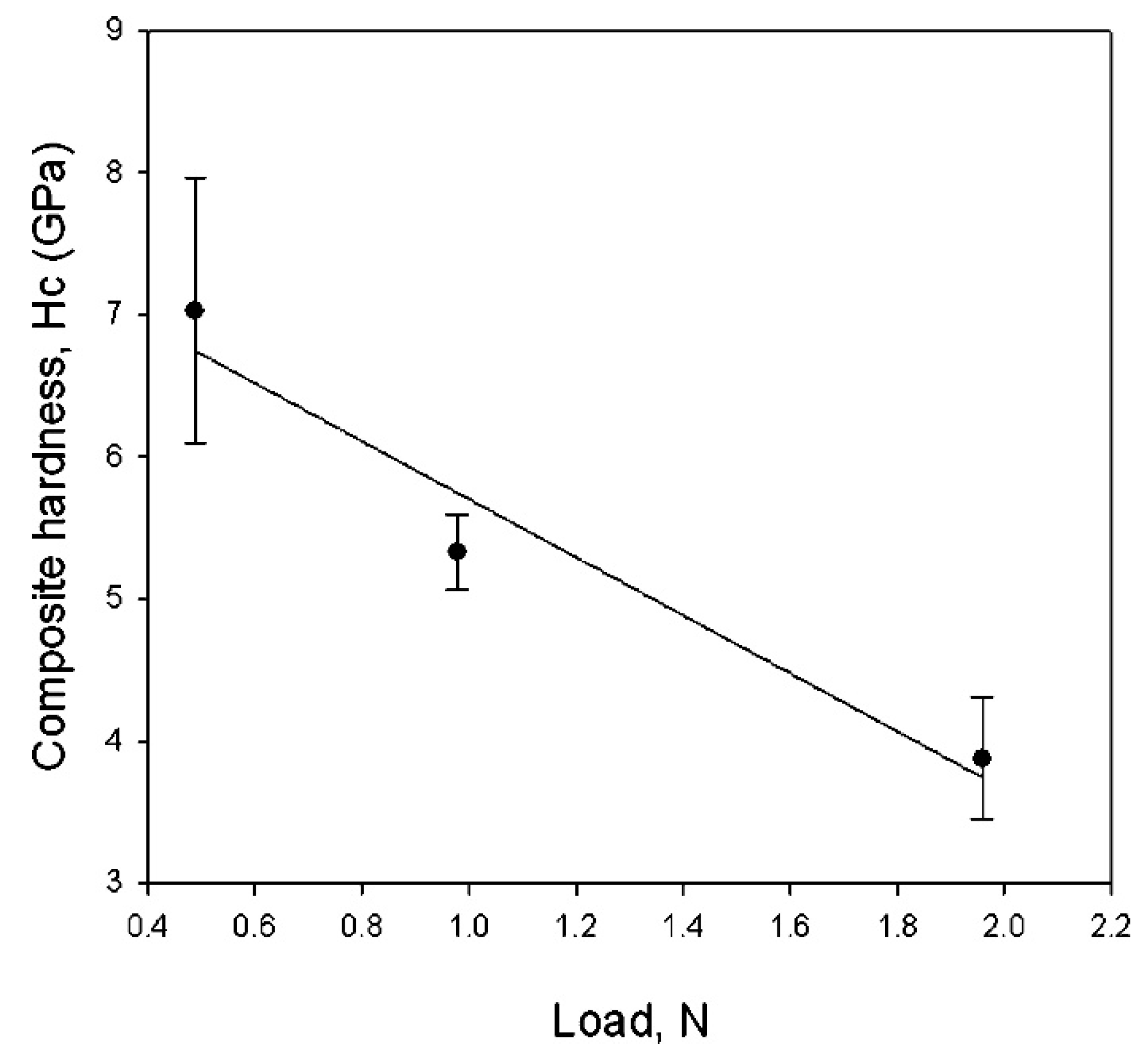
  81. Rau, J.V.; Ferro, D.; Falcone, M.B.; Generosi, A.; Rossi Albertini, V.; Latini, A.; Teghil, R.; Barinov, S.M. Hardness of zirconium diboride films deposited on titanium substrates. Mater. Chem. Phys. 2008, 112, 504–509. [Google Scholar] [CrossRef]
  82. Tamura, H.; Konoue, M.; Sawaoka, A.B. Zirconium boride and tantalum carbide coatings sprayed by electrothermal explosion of powders. J. Therm. Spray. Technol. 1997, 6, 463–468. [Google Scholar] [CrossRef]
  83. De Bonis, A.; Teghil, R.; Rau, J.V.; Galasso, A.; Orlando, S.; Santagata, A. Characterization of gaseous phase and nanoparticles produced in ultra-short pulsed laser ablation of transition metal borides. Appl. Surf. Sci. 2011, 257, 5315–5318. [Google Scholar] [CrossRef]
  84. Chung, H.; Weinberger, M.B.; Yang, J.; Tolbert, S.H.; Kaner, R.B. Correlation between hardness and elastic moduli of the ultraincompressible transition metal diborides RuB2, OsB2, and ReB2. Appl. Phys. Lett. 2008, 92, 261904. [Google Scholar] [CrossRef] [Green Version]
  85. Rau, J.V.; Latini, A.; Generosi, A.; Rossi Albertini, V.; Ferro, D.; Teghil, R.; Barinov, S.M. Deposition and characterization of superhard biphasic ruthenium boride films. Acta Mater. 2009, 57, 673–681. [Google Scholar] [CrossRef]
  86. Weinberger, M.B.; Levine, J.B.; Chung, H.; Cumberland, R.W.; Rasool, H.I.; Yang, J.; Kaner, R.B.; Tolbert, S.H. Incompressibility and Hardness of Solid Solution Transition Metal Diborides: Os1−xRuxB2. Chem. Mater. 2009, 21, 1915–1921. [Google Scholar] [CrossRef]
  87. Latini, A.; Rau, J.V.; Teghil, R.; Generosi, A.; Rossi Albertini, V. Superhard Properties of Rhodium and Iridium Boride Films. ACS Appl. Mater. Interfaces 2010, 2, 581–587. [Google Scholar] [CrossRef]
  88. Samsonov, G.V.; Kosenko, V.A.; Rud’, B.M.; Sidorova, V.G. Preparation and properties of the compound IrB1.1. Inorg. Mater. 1972, 8, 671–672. [Google Scholar]
  89. Zeiringer, I.; Cheng, X.; Chen, X.; Bauer, E.; Giester, G.; Rogl, P.F. Crystal structures and constitution of the binary system iridium-boron. Sci. China Mater. 2015, 58, 649–668. [Google Scholar] [CrossRef] [Green Version]
  90. Rau, J.V.; Latini, A.; Teghil, R.; De Bonis, A.; Fosca, A.; Caminiti, R.; Rossi Albertini, V. Superhard Tungsten Tetraboride Films Prepared by Pulsed Laser Deposition Method. ACS Appl. Mater. Interfaces 2011, 3, 3738–3743. [Google Scholar] [CrossRef]
  91. Schlesinger, M.E.; Liao, P.K.; Spear, K.E. The B-La (Boron-Lanthanum) System. J. Phase Equilib. 1999, 20, 73–78. [Google Scholar] [CrossRef]
  92. Lafferty, J.M. Boride Cathodes. J. Appl. Phys. 1951, 22, 299–309. [Google Scholar] [CrossRef]
  93. Bellucci, A.; Mastellone, M.; Orlando, S.; Girolami, M.; Generosi, A.; Paci, B.; Soltani, P.; Mezzi, A.; Kaciulis, S.; Polini, R.; et al. Lanthanum (oxy)boride thin films for thermionic emission applications. Appl. Surf. Sci. 2019, 479, 296–302. [Google Scholar] [CrossRef] [Green Version]
  94. Liao, P.K.; Spear, K.E. The B-Cr (boron-chromium) system. Bull. Alloy Phase Diagr. 1986, 7, 232–237. [Google Scholar] [CrossRef]
  95. Pierson, H.O. Handbook of Refractory Carbides and Nitrides; Noyes Publications: Westwood, CA, USA, 1996. [Google Scholar]
  96. Krajewski, A.; D’Alessio, L.; De Maria, G. Physico-chemical and thermophysical properties of cubic binary carbides. Cryst. Res. Technol. 1998, 33, 341–374. [Google Scholar] [CrossRef]
  97. Teghil, R.; D’Alessio, L.; De Bonis, A.; Galasso, A.; Villani, P.; Zaccagnino, M.; Santagata, A.; Ferro, D. Femtosecond pulsed laser ablation of group 4 carbides. Appl. Surf. Sci. 2005, 247, 51–56. [Google Scholar] [CrossRef]
  98. Ferro, D.; Rau, J.V.; Rossi Albertini, V.; Generosi, A.; Teghil, R.; Barinov, S.M. Pulsed laser deposited hard TiC, ZrC, HfC and TaC films on titanium: Hardness and an energy-dispersive X-ray diffraction study. Surf. Coat. Technol. 2008, 202, 1455–1461. [Google Scholar] [CrossRef]
  99. Andrievski, R.A.; Spivak, I.I. Strength of Refractory Compounds and Related Materials; Metallurgy: Tcheljabinsk, Russia, 1989. [Google Scholar]
  100. Teghil, R.; De Bonis, A.; Galasso, A.; Villani, P.; Santagata, A.; Ferro, D.; Barinov, S.M. Nanostructured thin films obtained by ultra-short pulse laser deposition of vanadium carbide. Appl. Surf. Sci. 2009, 255, 5220–5223. [Google Scholar] [CrossRef]
  101. Sansone, M.; De Bonis, A.; Santagata, A.; Rau, J.V.; Galasso, A.; Teghil, R. Pulsed laser ablation and deposition of niobium carbide. Appl. Surf. Sci. 2016, 374, 112–116. [Google Scholar] [CrossRef]
  102. Duhalde, S.; Colaco, R.; Audebert, F.; Perrone, A.; Zocco, A. Deposition of NbC thin films by pulsed laser ablation. Appl. Phys. A 1999, 69, S569–S571. [Google Scholar] [CrossRef]
  103. Teghil, R.; De Bonis, A.; Galasso, A.; Villani, P.; Santagata, A. Femtosecond pulsed laser ablation deposition of tantalum carbide. Appl. Surf. Sci. 2007, 254, 1220–1223. [Google Scholar] [CrossRef]
  104. Wallace, T.C.; Butt, D.P. Review of diffusion and vaporization of Group 4 and 5 transition metal carbides. In Chemistry of Transition Metal Carbides and Nitrides; Oyama, S.T., Ed.; Blackie Academic and Professional: Glasgow, UK, 1996; pp. 53–90. [Google Scholar]
  105. Avatbé, R.G. The thermodynamic stability of monocarbides of transition metals from sub groups IV–VI. Powder Metall. Met. Ceram. 1965, 4, 122–128. [Google Scholar]
  106. Jubair, M.; Tanveer Karim, A.M.M.; Nuruzzaman, M.; Zilani, M.A.K. Comparison of structural, mechanical and optical properties of tantalum hemicarbide with tantalum monocarbide: Ab initio calculations. J. Phys. Commun. 2019, 3, 055017. [Google Scholar] [CrossRef]
  107. Hackett, K.; Verhoef, S.; Cutler, R.A.; Shetty, D.K. Phase Constitution and Mechanical Properties of Carbides in the Ta–C System. J. Am. Ceram. Soc. 2009, 92, 2404–2407. [Google Scholar] [CrossRef]
  108. Doi, K.; Hiraishi, S.; Kawasaki, H.; Suda, Y. Preparation of Crystalline Chromium Carbide Thin Films Synthesized By Pulsed Nd:YAG Laser Deposition. Mater. Res. Soc. Symp. 2000, 617, J7.8. [Google Scholar] [CrossRef]
  109. Teghil, R.; Santagata, A.; De Bonis, A.; Galasso, A.; Villani, P. Chromium carbide thin films deposited by ultra-short pulse laser deposition. Appl. Surf. Sci. 2009, 255, 7729–7733. [Google Scholar] [CrossRef]
  110. De Bonis, A.; Santagata, A.; Sansone, M.; Rau, J.V.; Mori, T.; Teghil, R. Femtosecond pulsed laser ablation of molybdenum carbide: Nanoparticles and thin film characteristics. Appl. Surf. Sci. 2013, 278, 321–324. [Google Scholar] [CrossRef]
  111. Teghil, R.; De Bonis, A.; Galasso, A.; Sansone, M.; Rau, J.V.; Santagata, A. Nanostructured molybdenum carbide thin films obtained by femtosecond pulsed laser deposition. Phys. Status Solidi C 2012, 9, 2370–2373. [Google Scholar] [CrossRef]
  112. De Bonis, A.; Teghil, R.; Santagata, A.; Galasso, A.; Rau, J.V. Thin films deposited by femtosecond pulsed laser ablation of tungsten carbide. Appl. Surf. Sci. 2012, 258, 9198–9201. [Google Scholar] [CrossRef]
  113. Cappelli, E.; Bellucci, A.; Orlando, S.; Trucchi, D.M.; Mezzi, A.; Valentini, V. PLD deposition of tungsten carbide contact for diamond photodiodes. Influence of process conditions on electronic and chemical aspects. Appl. Surf. Sci. 2013, 278, 111–116. [Google Scholar] [CrossRef]
Figure 1. Experimental set-up for Pulsed Laser Deposition (PLD) experiments in vacuum or in gas pressure.
Coatings 10 00501 g001
Figure 2. ICCD images of the plume obtained using fs ablation of a C60 target: (a) delay 50 ns, gate 200 ns; (b) delay 250 ns, gate 200 ns; (c) delay 2 μs, gate 2 μs; (d) delay 15 μs, gate 2 μs. The dimensions of the rectangular areas are 1 × 1.6 cm. Reprinted with permission from [31]. Copyright 2013 Elsevier.
Coatings 10 00501 g002
Figure 3. FESEM images of a TiO2 film deposited in air: (a) 10,000× magnification; (b) 200,000× magnification. Reprinted with permission from [70]. Copyright from 2017 AIP Publishing.
Coatings 10 00501 g003
Figure 4. FESEM images representative of TiO2 films. Left panel: films deposited at p < 1 mbar; right panel: films deposited at p > 1 mbar. Lower panels report cross section of the same films. Reprinted with permission from [71], copyright 2013 Elsevier.
Coatings 10 00501 g004
Figure 5. Composite Vickers hardness of the film/substrate (ReB2/SiO2) system versus load. Considering the film thickness, the intrinsic hardness of the ReB2 film was 52 ± 6 GPa. Reprinted with permission from [78]. Copyright 2008 American Chemical Society.
Coatings 10 00501 g005
Figure 6. (a) XRD pattern and (b) Raman spectrum of LaB6 thin films deposited using fs PLD. Reprinted with permission from [93]. Copyright 2019 Elsevier.
Coatings 10 00501 g006
Figure 7. TEM microphotographs of (a) TiC film using a 5 min deposition at a distance of 2.0 cm from the target; (b) TiC film using a 30 min deposition at a distance of 2.0 cm. Reprinted with permission from [29], copyright 2006 Elsevier.
Coatings 10 00501 g007
Figure 8. XPS spectra of a Mo2C film deposited at 600 °C: (a) Mo 3d region, (b) C 1s region. Reprinted with permission from [111], copyright 2012 Wiley and Sons.
Coatings 10 00501 g008

