Article

Femtosecond Pulsed Laser Deposition of Chromium Diboride-Rich Thin Films

1
Dipartimento di Scienze, Università della Basilicata, Via dell’Ateneo Lucano 10, 85100 Potenza, Italy
2
Dipartimento di Chimica, Università di Roma la Sapienza, Piazzale Aldo Moro 5, 00185 Rome, Italy
3
Istituto di Struttura della Materia, Consiglio Nazionale Delle Ricerche, Via del Fosso del Cavaliere 100, 00133 Rome, Italy
4
Istituto di Struttura della Materia, Consiglio Nazionale Delle Ricerche, U.O.S. di Potenza, Zona Industriale di Tito Scalo, 85050 Tito Scalo (PZ), Italy
*
Author to whom correspondence should be addressed.
Coatings 2019, 9(12), 777; https://doi.org/10.3390/coatings9120777
Submission received: 24 October 2019 / Revised: 16 November 2019 / Accepted: 18 November 2019 / Published: 21 November 2019
(This article belongs to the Special Issue Surface Function Enhancement Film and Coating Technology)

Abstract

:
Chromium borides are promising candidates for several structural applications including protective coatings for materials exposed to corrosive and abrasive environments. In this paper the pulsed laser deposition of chromium diboride-rich thin films has been carried out in vacuum by using a frequency doubled Nd:glass laser with a pulse duration of 250 fs. The films have been deposited at different substrate temperatures and characterized by X-ray diffraction, X-ray photoelectron spectroscopy, scanning electron microscopy and transmission electron microscopy. Lastly, the film’s hardness has been studied by Vickers indentation technique. The results indicate that only the films deposited at a substrate temperature of 500 °C are crystalline and formed by chromium diboride, together with a certain amount of boron and chromium, which suggests that, as main mechanism, a process taking place on the surface from atoms and ions from the gas phase. This hypothesis has been confirmed by the study of the plasma produced by the ablation process.

1. Introduction

Transition metal borides have received a large scientific and technological interest in the recent years, due to their peculiar chemical-physics and mechanical properties [1,2]. Among these compounds, chromium borides are promising candidates for several structural applications such as protective coatings for materials exposed to corrosive and abrasive environments [3,4,5,6]. In the chromium-boron phase diagram there is evidence of the presence of six chromium borides, which include Cr2B, Cr5B3, CrB, Cr3B4, CrB2 and CrB4 [7]. Among these borides, chromium diboride (CrB2) is of particular interest, showing the higher melting temperature, a good electrical conductivity and a hardness of the order of 20 GPa [3,4,5,6,8,9]. For these characteristics chromium diboride is currently used in the form of coatings and thin films to increase the performance of cutting and forming tools, including improving their wear and corrosion resistance [4,6,10,11,12].
Chromium diboride thin films have been already deposited by several techniques including thermal evaporation process [11], magnetron sputtering in different configurations [4,6,9,12,13,14,15,16], chemical vapor deposition [17] and conversion treatment [18]. The results indicate that in some cases the films were boron-defective [9,11,14,15] while in others showed a brittle behavior [6,12,13] or needed particular requirements for the experimental apparatus [4]. In the case of the layers produced by conversion method, a mixture of CrB and CrB2 was obtained [18]. On the other hand, Pulsed Laser Deposition (PLD) is not only a quite simple physical deposition technique which, in general, does not require a post annealing treatment or the presence of a buffer gas, but it has already been successfully applied to the production of metal borides thin films. Indeed, the boride films produced by PLD showed a very high hardness. In particular, super-hard films have been obtained for RhB2 [19], ZrB2 [20], ruthenium, rhodium, and iridium borides [21,22,23]. In all cases the films were stoichimetric and only in the case of ZrB12 ablation biphasic films were obtained [24]. All those PLD experiments were performed by ultra-short pulse lasers, with the further advantage of obtaining nano-structured films, a peculiar characteristic of fs PLD [25], which often contributes to increase the films hardness. For these reasons ultra-shot PLD technique can be considered a suitable candidate for the deposition of chromium boride films.
The aim of this paper was to study the possibility to obtain chromium boride films in vacuum by ablating a target formed by mixed powders of boron and chromium utilizing an ultra short pulse laser. Considering the characteristics of the films deposited by fs PLD, our intention was to deposit nanostructured films and to verify the ablation-deposition mechanism for the boron-chromium system. Therefore, in this paper, chromium diboride-rich thin films have been obtained by PLD, using a laser source with a pulse duration of 250 fs. The use of a stoichiometric target (B/Cr molar ratio of 2:1) gave no results, likely due to a loss of boron, so a boron rich target (B/Cr molar ratio of 4:1) has been used for further experiments. Composition, morphology and crystallinity of the films have been characterized by different techniques and their hardness has been measured by the Vickers indentation method. To clarify the ablation-deposition mechanism, which was different from the typical mechanism proposed for fs PLD, the plasma produced by the laser-target interaction, in the case of a boron-rich target, has also been also studied.

2. Materials and Methods

The deposition experiments have been carried out by an apparatus already described [26]. It consists of a stainless steel vacuum chamber, evacuated to a pressure of 1.5 × 10⁻⁴ Pa, equipped with windows for the inlet of the laser beam and for the observation of plasma emission, together with a rotating target holder and heated substrate support. The experiments have been performed at substrate temperatures from 25 to 500 °C, and the distance between the target and the substrate was kept at 2.0 cm. The ablation source was a frequency doubled (λ = 527 nm) Nd:glass laser (Twinkle-Light Conversion) with a pulse duration of 250 fs and a repetition rate of 10 Hz. The laser fluence was kept at 2.8 J·cm−2 and the deposition time was 2 h for all films. The films were deposited on n-type Si (100) substrates with an area of 1.0 cm2. The substrates had a polished surface and no chemical etching process was carried out on the surface. The laser beam was incident at an angle of 45° on the target surface, and the targets were pellets obtained by pressing a mixture of boron (99.5% purity, Sigma Aldrich, St. Louis, MO, USA) and chromium (Sigma-Aldrich 99.95% purity) powders in 2:1 and 4:1 molar ratios. The pellets were subsequently annealed for 2 h at a temperature of 700 °C in Ar atmosphere.
The morphology of the films was analyzed by a high-resolution field emission scanning electron microscope (FESEM, AURIGA, Karl Zeiss, Oberkochen, Germany) while the films crystallinity was evaluated by X-ray diffraction (XRD, D5000, Siemens AG, Munich, Germany), using Cu Kα1 radiation. The first steps of the film’s growth were characterized by a high resolution transmission electron microscope (HR-TEM, Technai, FEI Company, Hillsboro, OR, USA) operating at 200 kV, and the material was deposited on formvar-coated copper grids. The composition of the films surface was studied by X-ray photoelectron spectroscopy (XPS, Phoibos 100 MCD, SPECS GmBH, Berlin, Germany), using un-monochromatized Mg Kα radiation.
Hardness measurements of the films were carried out by means of the Leica VMHT micro-hardness apparatus (Leica GmBH, Wetzlar, Germany) supplied with a standard Vickers pyramidal indenter (square-based diamond pyramid with a 136° face angle). The involved six loads ranged from 0.049 up to 0.981 N, applied for 15 s at the loading and unloading speed of 5×10⁻⁶ m/s. About 10–15 indentations were made at each load. Vickers hardness of the Si substrate was measured separately; it was found to be 10.2 ± 0.6 GPa. For the deposited films, the hardness, which was measured, corresponded to the film-substrate composite system. In order to extract from these experimental data the intrinsic film hardness, the Joensson and Hogmark approach was applied [27]. The procedure was described in detail in our previous studies [20,28].
The optical emission spectra (OES) were detected using a bundle of 19 fused silica fibers, linked to a 500-mm focal length spectrograph (ARC 500i, Acton Research Corporation, Acton, MA, USA), connected to an ICCD 1024 × 1024 pixels device (Princeton Instruments, Trenton, NJ, USA). The spectrograph was equipped with two different gratings, with 1200 and 150 grooves/mm. The spectra were detected ranging from 250 to 800 nm. The gated system had a best time resolution of 2 ns, and each acquisition was integrated over 20 laser shots in order to increase the signal-to-noise ratio. By varying the position of the optical elements by a micrometric translation stage, it has been possible to obtain space-resolved emission spectra at different distances from the ablated target surface. The same ICCD system, equipped with 105/35 mm quartz Nikkor lenses, was used for acquiring gated lateral view images of the overall plasma emission induced by a single laser pulse. ICCD fast imaging and time-resolved spectra were accomplished by delaying the data acquisition of the plasma emission with respect to the laser pulse. Both optical emission and fast ICCD imaging measurements were carried out without the presence of the substrate.

3. Results and Discussion

The XRD spectra of the films deposited from the target with a B/Cr molar ratio of 2:1 indicate that the films are amorphous, independently from the substrate temperature. The XPS spectra of the films deposited at room temperature, 300 and 500 °C show the same features, i.e., the presence of only B, B2O3 and Cr2O3, which indicate that, independently from the substrate temperature, no Chromium-Boron compounds are present in the films. As an example, the XPS spectra of a film deposited at a substrate temperature of 500 °C are reported in Figure 1. The B1s region presents two peaks centered at 192.1 and 187.4 eV, assigned to B2O3 and B species, respectively [29,30,31,32]. In Cr 2p region, the Cr 2p3/2 signal has been fitted with three peaks at 576.6, 577.2 and 578.4 eV, which can be related to Cr2O3 species [33,34,35].
Considering the total B-Cr ratios obtained from XPS data (B/Cr = 0.65), it is evident that in the films there is a deficiency of boron with respect to the target composition. Clearly, this means that the ablation-deposition process, independently from the substrate temperature, produces a boron preferential loss. A preferential loss of light elements was reported for PLD experiments but only in the case of the use of ns laser sources [36,37], where the main deposition mechanism is condensation from the gas phase.
To try to counterbalance the boron deficiency found in the films, a boron-richer target (B-Cr molar ratio = 4:1) was prepared and used for further ablation-deposition experiments.

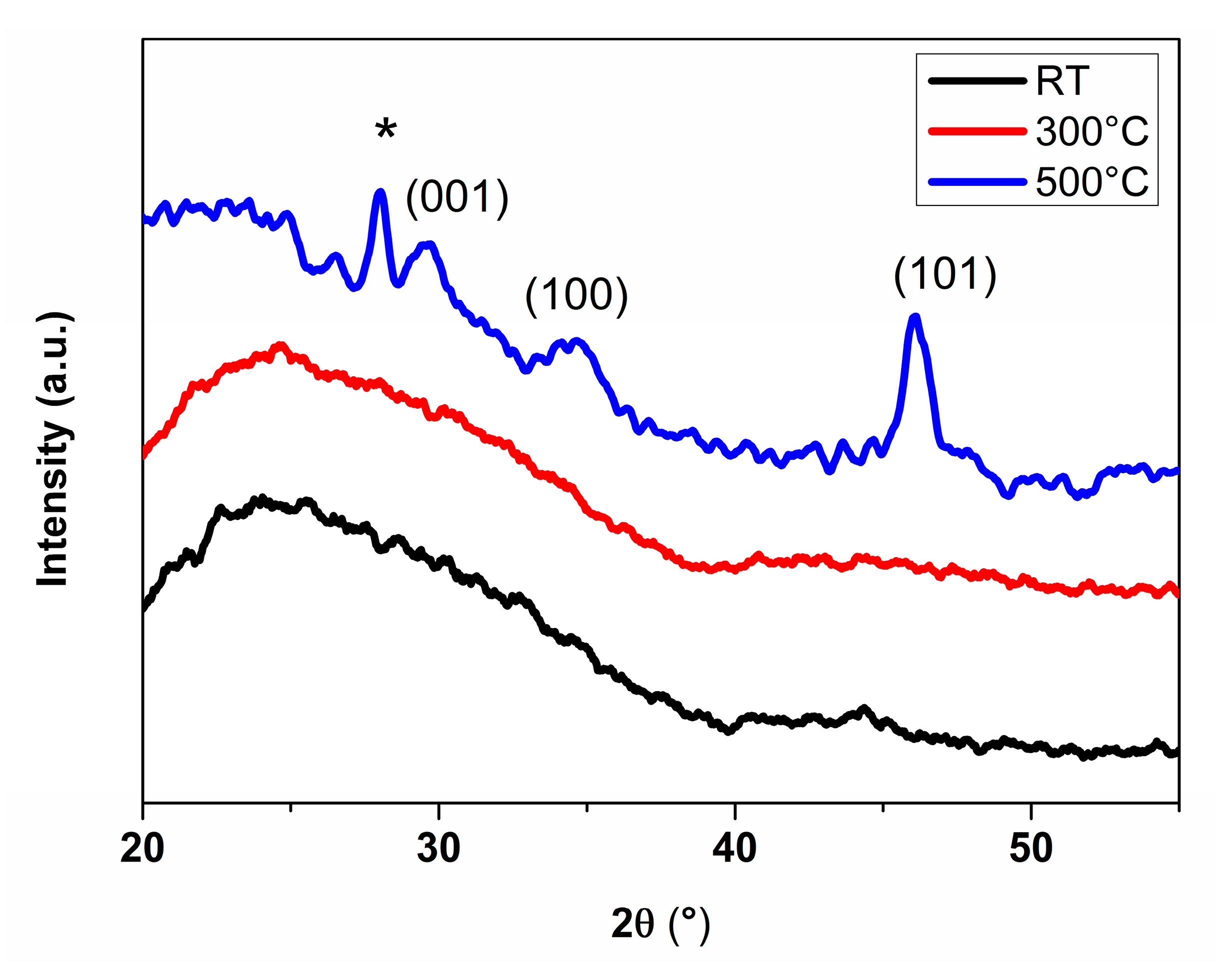
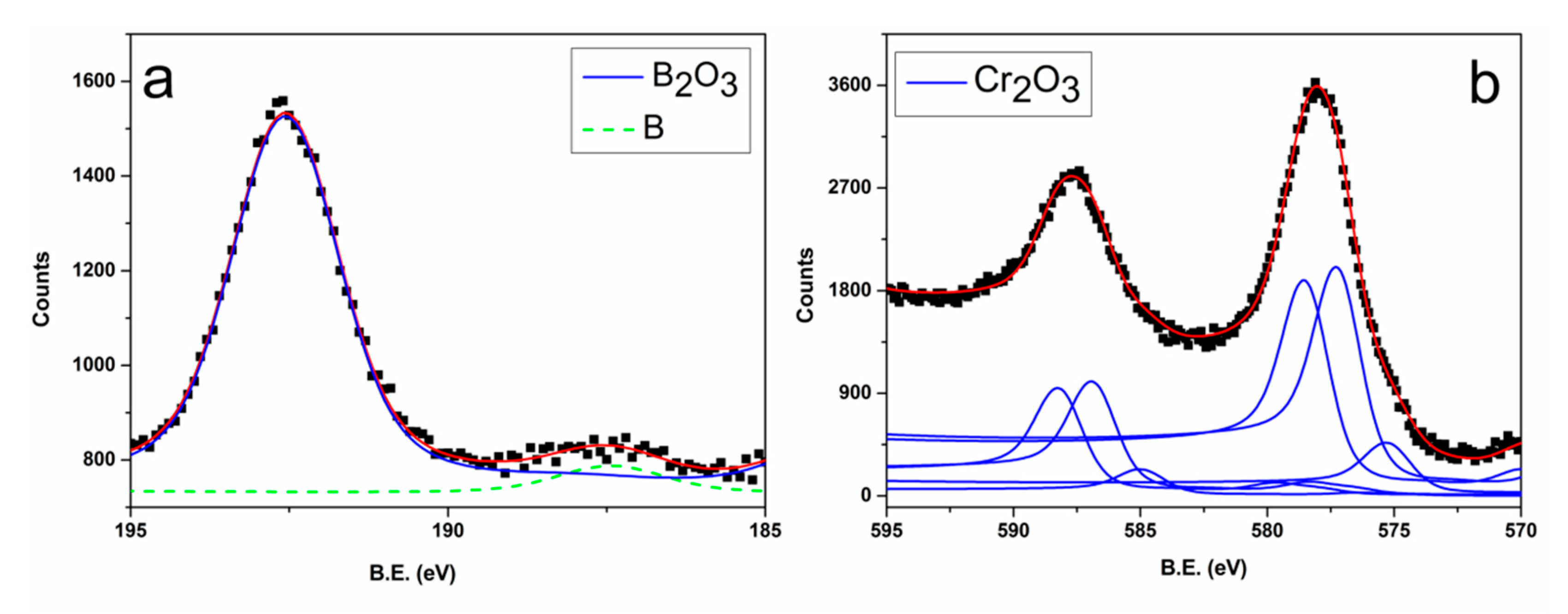
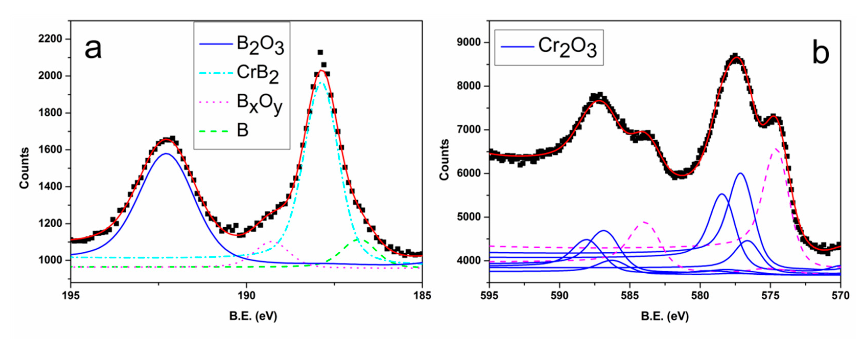
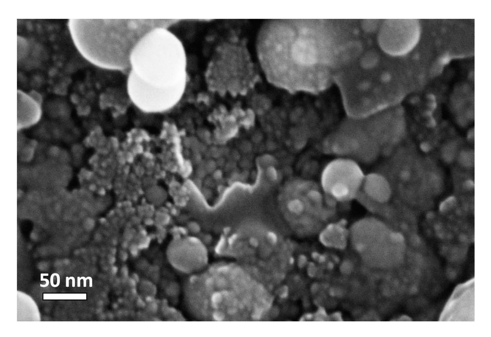
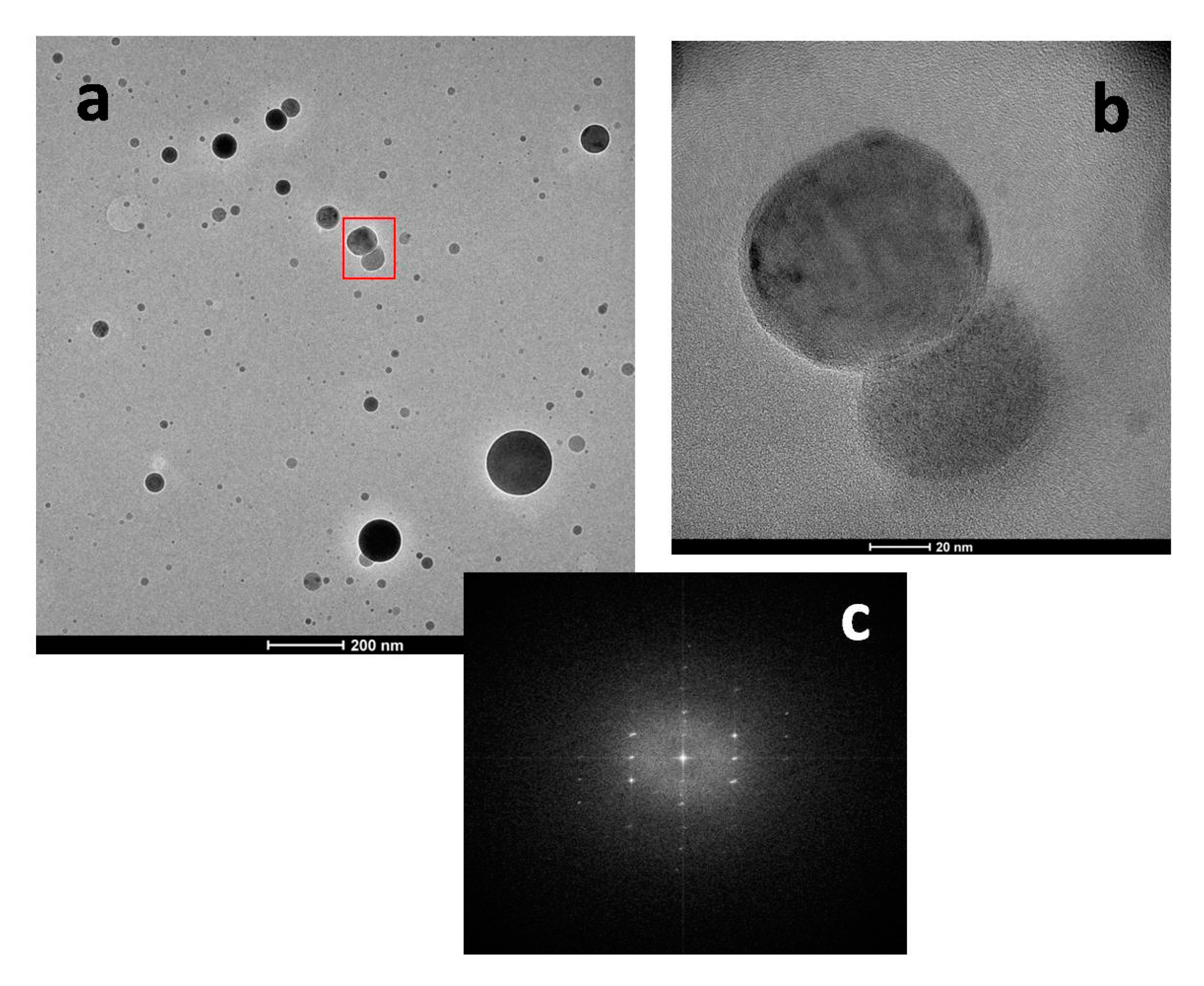
3.1. Films Characterization
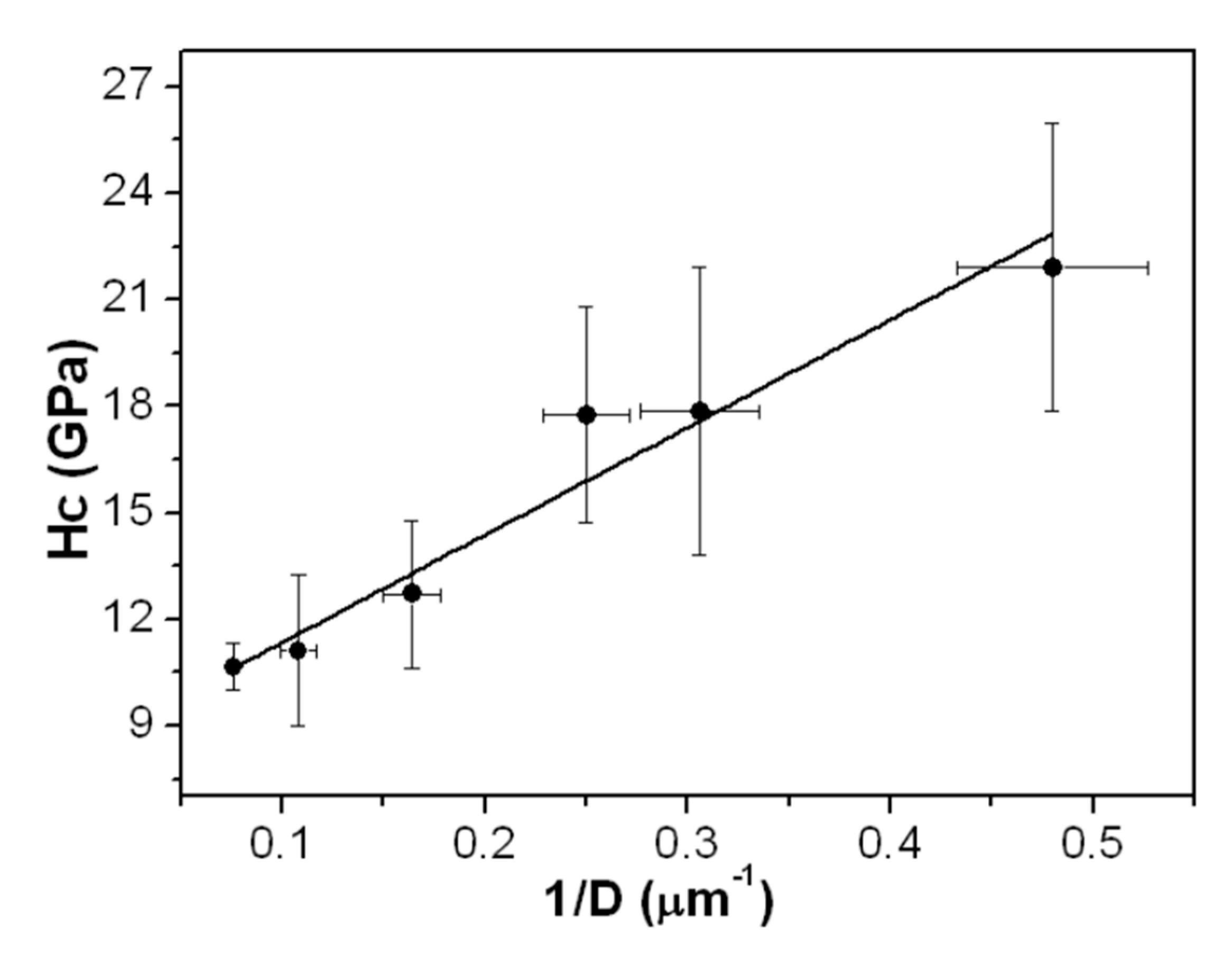
The XRD spectra of the films deposited at 25 and 300 °C show that these are amorphous (Figure 2). On the other hand, the spectrum of the film deposited at a substrate temperature of 500 °C (Figure 2) show broad peaks assigned to (001), (100) and (101) planes of hexagonal CrB2 (PDF 00-034-0369 (ICDD, 2005)) [38]. The peak at 2θ = 27° does not belong to CrB2 and can be assigned to the B2O3 (310) plane (PDF 00-006-0297 (ICDD, 2005)) [38]. The presence of boron oxide is not surprising since a certain amount of boron oxide was already present in the ablation target. The features of the spectra indicate that the film at 500 °C still presents a certain amorphous component.
For a further characterization of the composition of the films, we have used the XPS technique. In the films deposited at room temperature, the analysis of the B 1s region (Figure 3a) shows the presence of two contributes at 187.4 eV and 192.5 eV. These contributes are assigned to atomic boron and B2O3, respectively [29,30,31,32]. In the Cr 2p region (Figure 3b), the doublet centered at 578.7 and 588.4 eV is assigned to Cr2O3 [29,33,34,35,39,40,41]. In these films there is no evidence of the presence of chromium borides. The XPS spectra of the films deposited at a substrate temperature of 300 °C arevery similar (Figure 4), which show, in the B 1s region, the presence of atomic boron (187.3 eV) and B2O3 (192.4 eV) and, in the Cr 2p region, only the presence of Cr2O3. This is different from the situation for the films deposited at 500 °C. The XPS spectrum of the B 1s region (Figure 5a) shows four signals, two attributed to atomic boron (186.8 eV) and CrB2 (187.9 eV) [29,42,43], and the other two to a non-stoichiometric boron oxide BxOy (189.3 eV) and to B2O3 (192.3 eV).
In the Cr 2p region, a new component at lower binding energy with respect to Cr2O3 can be observed. This shoulder has been fitted by a doublet with components centered at 574.5 and 583.9 eV, respectively, and has been assigned to CrB2 [42]. The stoichiometry of the chromium-boron compound, obtained by the XPS data (peak at 187.9 eV in the B 1s region and peaks, at 574.5 and 583.9 eV in the Cr 2p region) corresponds to CrB2.4, which could refer both to a non-stoichiometric chromium diboride or to a mixture of chromium diboride and chromium tetraboride.
The morphology of the films deposited at different substrate temperatures is shown in Figure 6.
In all cases the films seem to be formed by the coalescence of particles with a nanometric size, but some differences can be shown. In the film deposited at room temperature (Figure 6a), the presence of a compact matrix above which nano and micro particles are superimposed is evident. Some of these particles are clearly molten material ejected from the target. In the case of the films deposited at 300 °C (Figure 6b), there is an increase of the number of nanoparticles (NPs) which become the main components of the films deposited at 500 °C (Figure 6c).
The high-resolution FESEM micrograph of a film deposited at 500 °C (Figure 7) confirms that the NPs are the main components of the film. It clearly shows the presence of both small NPs (less than 10 nm in diameter) and of larger particles. These larger particles are evidently deposited as melted material.
To study the first steps of the films growth, HR-TEM analyses have been carried out. The materials have been deposited for 5 min on holey carbon-coated copper grids. Therefore, the experiments have been carried out only at room temperature.
HR-TEM images (Figure 8a) show the presence of two types of particles: larger particles, with diameters in the range of 60–80 nm and smaller ones with 10-nm diameters. Some of the larger particles contain nanometric crystalline domains, as shown in Figure 8b. The diffraction spots present in the 2D Fast Fourier Transform (FFT) image (Figure 8c) allow the evaluation of the lattice spacings. The values of 0.28, 0.50, 0.55 and 0.87 nm correspond to the lattice spacings of (125), (104), (110), and (101) planes of boron, respectively. The less intense spots at 0.19, 0.25 and 0.31 nm correspond to the lattice spacings of (101), (100) and (001) planes of CrB2, respectively. In general, CrB2 crystalline domains are present in few NPs, where the larger part contains only boron.

3.2. Films Hardness

In order to characterize the mechanical properties of the CrB2 films deposited at 500 °C, the Vickers microhardness tests were carried out. The obtained results on measurements of the composite hardness (Hc) of the film-substrate composite system versus the inverse imprint diagonal (1/D) are shown in Figure 9. Using these experimental data and the Joensson and Hogmark approach [27], the intrinsic film hardness was found to be 21 ± 4 GPa, in which thickness was 200 nm. This value is somewhat higher than the Vickers hardness for the CrB2bulk material, where the latter was 16–20 GPa [3,6,8,9]. This is likely due to the nanocrystalline nature of the 500 °C deposited film.

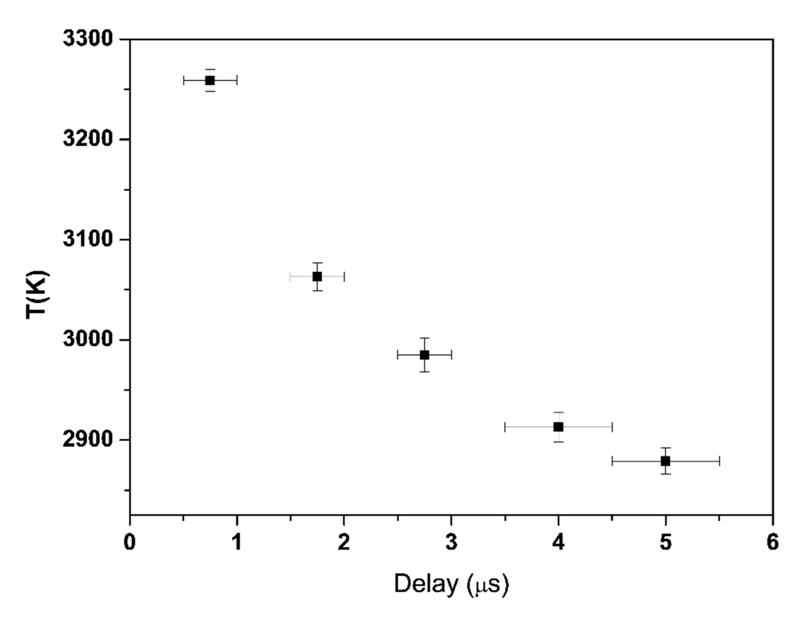
3.3. Plasma Analysis

To clarify the reasons of the particular characteristics of the deposited films, the plasma produced by the ablation of the target with B/Cr molar ratio of 4:1 has been studied.
As already found for fs ablation, not only of metal borides [24,44,45] but also of other materials [25,46,47], OES show the presence of two different emissions that are completely separate temporally. The first emission (primary plume) develops after the end of the laser pulse and is quenched after 600 ns. The emission spectrum is formed by several lines assigned to Cr I, Cr II and B II. Neutral boron emission has not been detected since it was outside the wavelength range of our apparatus (250–800 nm).
After the first μs from the laser pulse, a second emission (secondary plume) has been detected. This plume shows a black-body like continuous spectrum, likely due to the emission of nanoparticles or large clusters. The time duration of this plume is of the order of 20 μs. By using the Planck equation, in the Wien approximation for optical frequencies, in the form Iλε(1/λ4)ehc/λkBT (Iλ is the radiation intensity, ɛ the particle emissivity, λ the wavelength, T the temperature and kB the Boltzmann constant) and considering, in the Mie approximation, ε∝1/λ [48] the temperature of the particles forming the secondary plume and its temporal evolution have been calculated from the time evolution of the emission spectra. As can be seen from Figure 10, an initial temperature (500 ns after the laser pulse, with a gate of 500 ns) of about 3250 K, which decreases down to about 2900 K after 5 μs, has been obtained. This temperature decrease is similar to those observed for other systems, like transition metal borides, carbides and oxides, ablated by fs laser sources [44,47,49], with the main cooling contribution, in this range of temperature and in this time scale, being due to thermal vaporization from the particles.
Fast ICCD imaging has been used to obtain the lateral view images, at different time delays, of both primary and secondary expanding plumes. Plasma plume angular distributions have been calculated from ICCD images by considering the expression I(θ) = I0cosn(θ), where I(θ) is the flux intensity along a direction forming an angle θ. The normal to the target surface, I0 is the intensity corresponding to θ = 0, and n is a parameter related to the anisotropy of the angular distribution [50,51]. The results give n = 2.7 for the primary plume and n = 14.4 for the secondary one. Figure 11 shows the ICCD intensity contour patterns of primary and secondary plumes, obtained at delays of 100 ns and 2 μs after the laserpulse, respectively.
At a very long time delay after the laser pulse (30 μs and more) a third ejection of emitting material ta third ejection of emitting material from the target has been detected by fast ICCD imaging. As shown in Figure 12, this emission is due to large fragments, likely of micrometric size, ejected directly from the target. This kind of emission has been already detected for other systems [24,52] and is likely related to the relatively high laser fluence used in our experiments [52].

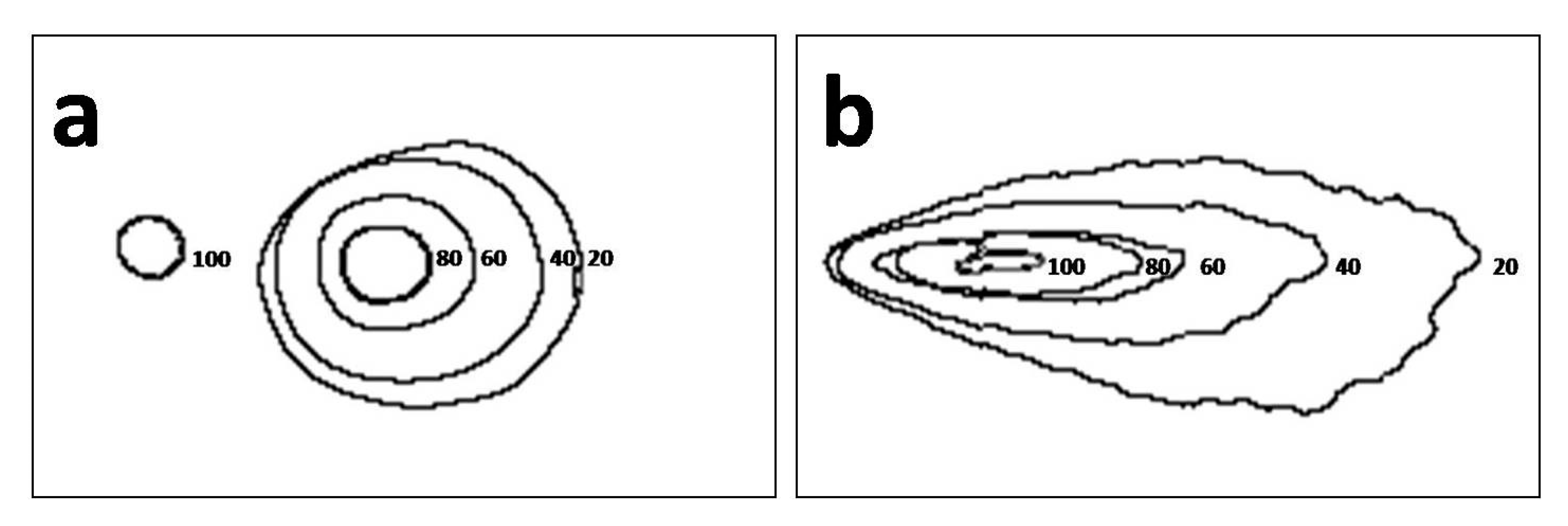
3.4. Ablation-Deposition Mechanism

In general, in the case of fs PLD, the main mechanism of the films formation seems to be related to the deposition on the substrate of a large number of NPs. Up to now, the origin of these NPs has not been completely clarified but, although their origin from condensation inside the plasma cannot be excluded [52,53], they are likely ejected directly from the target [25,47,54,55,56]. In this hypothesis, the stoichiometry of the deposited films should be influenced by the preferential evaporation from the NPs, with a loss of the elements having a higher partial vapor pressure [24,47,57].
In the case of the Cr-B system, the described ablation-deposition mechanism does not seem to completely match the experimental data. First of all, considering that the equilibrium vapor pressures of Cr and B are very different (at 2000 °C the Cr/B vapor pressures ratio is about 103) [58] and considering an initial congruent ablation, during the flight from the target to the substrate the NPs should lose chromium, which results in boron-rich films. This is the situation encountered, for example, in fs PLD of chromium carbide [49]. Instead, the experimental data about the deposit’s composition evidence, in our case, shows a different situation, with films always having a strong boron deficiency if compared to the target composition. Secondly, the presence of chromium boride in the films is clearly related to the substrate temperature. A film containing chromium boride is formed only at a substrate temperature of 500 °C and this behavior is typical of films formed by gas phase condensation on the substrate surface rather than by NPs deposition [59].
A possible explanation could be the one proposed by Trelenberg et al. [60] consisting in a preferential evaporation from the target of the elements with the higher vapor pressures, which is followed by their deposition on the substrate. On the other hand, XPS analysis of the ablated target indicates that the target stoichiometry is retained after the ablation. In fact, in the case of an initial total B:Cr ratio of 4:1, the XPS data, obtained from the B 1s and Cr 2p regions, show a final total ratio, of the ablated surface of the target, of 3.8:1. On the contrary, the Trelenberg hypothesis should require an ablated target enriched in the less volatile element, which is in our case boron.
The presence, in the plasma produced from the ablation of the Cr-B target, of three different emissions of material is an indication that the origin of the deposits could be related to both condensation of the gas phase forming the primary plume, the deposition of particles forming the secondary plume, and the third delayed one. In general, the studies on the relative contribution of the materials forming the primary and secondary plumes to the film formation report that the larger contribution is due to the NPs forming the latter one, with the gas phase primary plume playing a more limited role [55,56,61]. However, these studies refer only to metals (Au, Cu, Al) and for different systems the relative contributions could be different.
Our hypothesis is that for the boron-chromium system the primary plume plays a predominant role in the deposition process and, in this hypothesis, its behavior could be similar to that of the plume produced by ns ablation, with the film growth due mainly to gas phase condensation on the substrate. In the case of ns ablation, the loss of the light elements, which is in our case boron, also favored by the relatively low plume directionality, and is well documented in literature [36,37]. This hypothesis is also confirmed by the experimental conditions needed to obtain diboride films. Indeed, as already remarked, diboride films have been obtained only with a substrate temperature of 500 °C and this behavior is typical of films where growth is due to atoms or molecules coming from the gas phase and diffusing and reacting on the surface [59].
From this point of view, the growth of the films should take place following the mechanisms already proposed for the ablation performed by short pulse lasers, derived in turn from sputtering models [62,63]. In particular, the microstructure of the film can be described following the zone model [63] which permits a prevision of the film microstructure considering process parameters such as buffer gas pressure and substrate temperature. Taking into account that in our case the deposition was carried out in vacuum, the important parameter is the substrate temperature in the form T/Tm, where T is the substrate temperature and Tm is the melting point of the deposited material, both in Kelvin [63]. In the case of the films deposited at 500 °C, the value of T/Tm for chromium diboride is 0.42. The T/Tm, value is inside the zone 2 of the models proposed by Thornton (sputtering) [62,64] and by Movchan et al. (vapor deposition) [65]. In this zone we are in a regime where the surface diffusion is significant and it is not surprising that the probability that boron and chromium atoms could interact and coalesce on the surface is higher than that for lower substrate temperature. The T/Tm values for room temperature and 300 °C are 0.16 and 0.31 respectively, corresponding to zone T (Thornton) and zone 1, where the surface diffusion is negligible. The surface diffusion is only one of the parameters and the concentration of mobile atoms on the surface play also an important role and, from this point of view, in the case of the ablation of a 2:1 target the flux of boron atoms reaching the surface was too low to induce the formation of chromium boride even if the temperature of the substrate was high (500 °C).
In the hypothesis of a film composed mainly by condensation from the gas phase, the NPs forming the secondary plume will play a less important role. About their composition, even considering that they are initially formed by both Cr and B, they should be richer in boron with respect to the target composition, and this is confirmed by the TEM analyses (see Figure 7), which illustrates that the larger NPs show the presence of boron and only traces of chromium boride. In addition, the particles forming the secondary plume should arrive on the substrate as melted material. In fact, considering that the front velocity of the secondary plume, calculated by ICCD images, is 5.0 × 105 cm·s−1, and the distance between the target and the substrate is 2.0 cm. The secondary plume will arrive onto the substrate after about 4 μs from the laser pulse. Taking into account that the secondary plume temperature after 4 μs is about 2900 K (see Figure 10) and that the melting temperatures of boron, chromium and chromium diboride are 2349, 2130 and 1823 K respectively, this means that the NPs arriving on the substrate will be in the form of melted material. The FESEM image reported in Figure 7 clearly shows this melted material for the film is deposited at 500 °C. Considering that these molten NPs contribute to the final composition of the films, in the case of the films deposited at 500 °C (target B-Cr molar ratio = 4:1), they likely increase the boron content of the films themselves.

4. Conclusions

In conclusion, it is possible to obtain thin films of chromium diboride by PLD performed by a laser with a pulse duration of 250 fs, but only when the ablation target contains an excess of boron with respect to the stoichiometric value. Films containing boride with a stoichiometry corresponding to CrB2.4 have been obtained by using ablation targets with a Cr-B molar ratio of 1:4, even if elemental boron and chromium are also present. Another crucial parameter for the deposition is the substrate temperature. In fact, the formation of chromium diboride has been obtained only with a substrate temperature of 500 °C. These experimental conditions seem to indicate that chromium diboride is formed through a mechanism involving condensation and reaction of the gas phase species on the substrate surface rather than the coalescence of NPs, ejected from the target or formed by nucleation in the plasma, which is the typical mechanism of fs PLD. Lastly, the micro-hardness of the films deposited at 500 °C was found to be 21 ± 4 GPa.

Author Contributions

Conceptualization, R.T. and A.D.B.; Methodology, A.D.B., A.G. and A.S.; Validation, A.D.B., A.G. and A.L.; Investigation, A.D.B., M.C. and J.V.R.; Resources, A.L.; Data curation, A.D.B., M.C. and J.V.R.; Writing—review and editing, R.T. and A.S.; supervision, R.T.

Funding

This research received no external funding.

Acknowledgments

The authors thank Serena Pepe for performing some of the measurements and for helpful discussions.

Conflicts of Interest

The authors declare no conflict of interest.

References

  1. Carenco, S.; Portehault, D.; Boissiere, C.; Mezailles, N.; Sanchez, C. Nanoscaled metal borides and phosphides: Recent developments and perspectives. Chem. Rev. 2013, 113, 7981–8065. [Google Scholar] [CrossRef] [PubMed]
  2. Grechnev, G.E.; Fedorchenko, A.V.; Logosha, A.V.; Panfilov, A.S.; Svechkarev, I.V.; Filippov, V.B.; Lyashchenko, A.B.; Evdokimova, A.V. Electronic structure and magnetic properties of transition metaldi borides. J. Alloy. Compd. 2009, 481, 75–80. [Google Scholar] [CrossRef]
  3. Wang, S.; Yu, X.; Zhang, J.; Wang, L.; Leinenweber, K.; Xu, H.; Popov, D.; Park, C.; Yang, W.; He, D.; et al. Crystal structures, elastic properties, and hardness of high-pressure synthesized CrB2 and CrB4. J. Superhard Mater. 2014, 36, 279–287. [Google Scholar] [CrossRef]
  4. Audronis, M.; Kelly, P.J.; Arnell, R.D.; Leyland, A.; Matthews, A. The structure and properties of chromium diboride coatings deposited by pulsed magnetron sputtering of powder targets. Surf. Coat. Technol. 2005, 200, 1366–1371. [Google Scholar] [CrossRef]
  5. Qin, L.; Zhang, X.; Liang, Y.; Zhang, E.; Gao, H.; Zhang, Z. Preparation and characterization of nanocrystalline chromium boride. J. Mater. Sci. 2006, 41, 7617–7619. [Google Scholar] [CrossRef]
  6. Dahm, K.L.; Jordan, L.R.; Haase, J.; Dearnley, P.A. Magnetron sputter deposition of chromium diboride coatings. Surf. Coat. Technol. 1998, 108, 413–418. [Google Scholar] [CrossRef]
  7. Liao, P.K.; Spear, K.E. The B-Cr (boron-chromium) system. Bull. Alloy Phase Diagr. 1986, 7, 232–237. [Google Scholar] [CrossRef]
  8. Okada, S.; Kudou, K.; Iizumi, K.; Kudaka, K.; Higashi, I.; Lundström, T. Single-crystal growth and properties of CrB, Cr3B4, Cr2B3 and CrB2 from high-temperature aluminum solutions. J. Cryst. Growth 1996, 166, 429–435. [Google Scholar] [CrossRef]
  9. Nedfors, N.; Primetzhofer, D.; Wang, L.; Lu, J.; Hultman, L.; Jansson, U. Characterization of magnetron sputtered Cr-B and Cr-B-C thin films for electrical contact applications. Surf. Coat. Technol. 2015, 266, 167–176. [Google Scholar] [CrossRef]
  10. Jordan, L.R.; Betts, A.J.; Dahm, K.L.; Dearnley, P.A.; Wright, G.A. Corrosion and passivation mechanism of chromium diboride coatings on stainless steel. Corros. Sci. 2005, 47, 1085–1096. [Google Scholar] [CrossRef]
  11. Jha, M.; Marka, S.; Ghanashya, M.; Krishna, M.; Ganguli, A.K. Multifunctional nanocrystalline chromium boride thin films. Mater. Lett. 2012, 73, 220–222. [Google Scholar]
  12. Wenga, J.; Zuo, X.; Liu, L.; Wang, Z.; Ke, P.; Wei, X.; Wang, A. Dense nanocolumnar structure induced anti-corrosion CrB2 coating with (001) preferred orientation deposited by DC magnetron sputtering. Mater. Lett. 2019, 240, 180–184. [Google Scholar] [CrossRef]
  13. Zhang, S.; Wang, Z.; Guo, P.; Ke, P.; Odén, M.; Wang, A. Temperature induced superhard CrB2 coatings with preferred (001) orientation deposited by DC magnetron sputtering technique. In Pulsed Laser Deposition of thin Films; Chrisey, D.B., Hubler, G.K., Eds.; John Wiley & Sons: New York, NY, USA, 1994; pp. 229–264. [Google Scholar]
  14. Zhou, M.; Nose, M.; Makino, Y.; Nogi, K. New Cr-B hard coatings by r.f.-plasma assisted magnetron sputtering method. Thin Solid Film 1999, 343–344, 234–237. [Google Scholar] [CrossRef]
  15. Zhou, M.; Nose, M.; Makino, Y.; Nogi, K. Annealing effects on the structure and mechanical properties of r.f.-sputtered Cr-B hard thin films. Thin Solid Film 2000, 359, 165–170. [Google Scholar] [CrossRef]
  16. Choi, H.S.; Park, B.; Lee, J.J. CrB2 coatings deposited by inductively coupled plasma assisted DC magnetron sputtering. Surf. Coat. Technol. 2007, 202, 982–986. [Google Scholar] [CrossRef]
  17. Jayaraman, S.; Klein, E.J.; Yang, Y.; Kim, D.Y.; Girolami, G.S.; Abelson, J.R. Chromium diboride thin films by low temperature chemical vapor deposition. J. Vac. Sci. Technol. A 2005, 23, 631–633. [Google Scholar] [CrossRef]
  18. Boubaaya, R.; Benarioua, Y.; Allaoui, O.; Djendel, M. Production of chromium boride layers on carbon steel with conversion treatment: Chromium deposition+diffusion annealing. Acta Phys. Pol. A 2017, 132, 541–543. [Google Scholar] [CrossRef]
  19. Latini, A.; Rau, J.V.; Ferro, D.; Teghil, R.; Rossi Albertini, V.; Barinov, S.M. Superhard rhenium diboride films: Preparation and characterization. Chem. Mater. 2008, 20, 4507–4511. [Google Scholar] [CrossRef]
  20. Rau, J.V.; Ferro, D.; Falcone, M.B.; Generosi, A.; Rossi Albertini, V.; Latini, A.; Teghil, R.; Barinov, S.M. Hardness of zirconium diboride films deposited on titanium substrates. Mater. Chem. Phys. 2008, 112, 504–509. [Google Scholar] [CrossRef]
  21. Rau, J.V.; Latini, A.; Generosi, A.; Rossi Albertini, V.; Ferro, D.; Teghil, R.; Barinov, S.M. Deposition and characterization of superhard biphasic ruthenium borides films. Acta Mater. 2009, 57, 673–681. [Google Scholar] [CrossRef]
  22. Latini, A.; Rau, J.V.; Teghil, R.; Generosi, A.; Rossi Albertini, V. Superhard properties of rhodium and iridium boride films. ACS Appl. Mater. Interfaces 2010, 2, 581–587. [Google Scholar] [CrossRef] [PubMed]
  23. Rau, J.V.; Latini, A.; Teghil, R.; DeBonis, A.; Fosca, M.; Caminiti, R.; Rossi Albertini, V. Superhard properties of tungsten tetraboride films. ACS Appl. Mater. Interfaces 2011, 3, 3738–3743. [Google Scholar] [CrossRef] [PubMed]
  24. De Bonis, A.; Santagata, A.; Rau, J.V.; Latini, A.; Mori, T.; Medici, L.; Teghil, R. Two-phase zirconium boride thin film obtained by ultra-short pulsed laser ablation of a ZrB12 target. App. Surf. Sci. 2013, 283, 715–721. [Google Scholar] [CrossRef]
  25. Balling, P.; Schou, J. Femtosecond laser ablation dynamics of dielectrics: Basics and applications for thin films. Rep. Prog. Phys. 2013, 76, 036502. [Google Scholar] [CrossRef]
  26. D’Alessio, L.; Teghil, R.; Zaccagnino, M.; Zaccardo, I.; Ferro, D.; Marotta, V. Pulsed laser ablation and deposition of bioactive glass as coating material for biomedical applications. Appl. Surf. Sci. 1999, 138/139, 527–532. [Google Scholar]
  27. Joensson, B.; Hogmark, S. Hardness measurements of thin films. Thin Solid Film 1984, 114, 257–269. [Google Scholar] [CrossRef]
  28. Ferro, D.; Barinov, S.M.; Rau, J.V.; Latini, A.; Scandurra, R.; Brunetti, B. Vickers and Knoop hardness of electron beam deposited ZrC and HfC thin films on titanium. Surf. Coat. Technol. 2006, 200, 4701–4707. [Google Scholar] [CrossRef]
  29. NIST X-ray Photoelectron Spectroscopy (XPS) Database; Version 4.1; National Institute of Standards and Technology: Gaithersburg, MD, USA, 2012.
  30. Ennaceur, M.M.; Terreault, B. XPS study of the process of oxygen gettering by thin films of PACVD boron. J. Nucl. Mater. 2000, 280, 33–38. [Google Scholar] [CrossRef]
  31. Li, R.; Dong, G.; Chen, G. Synthesis, characterization and performance of ternary doped Cu-Ce-B/TiO2 nanotubes on the photocatalytic removal of nitrogen oxides. New J. Chem. 2015, 39, 6854–6863. [Google Scholar] [CrossRef]
  32. Xu, T.T.; Zheng, J.; Wu, N.; Nicholls, A.W.; Roth, J.R.; Dikin, D.A.; Ruoff, R.S. Crystalline boron nanoribbons: synthesis and characterization. Nano Lett. 2004, 4, 963–968. [Google Scholar] [CrossRef]
  33. Unveren, E.; Kemnitz, E.; Hutton, S.; Lippitz, A.; Unger, W.E.S. Analysis of highly resolved X-ray photoelectron Cr2p spectra obtained with a Cr2O3 powder sample prepared with adhesive tape. Surf. Interface Anal. 2004, 36, 92–95. [Google Scholar] [CrossRef]
  34. Payne, B.P.; Biesinger, M.C.; McIntyre, N.S. X-ray photoelectron spectroscopy studies of reactions on chromium metal and chromium oxide surfaces. J. Electron Spectrosc. 2011, 184, 29–37. [Google Scholar] [CrossRef]
  35. Biesinger, M.C.; Brown, C.; Mycroft, J.R.; Davidson, R.D.; McIntyre, N.S. X-ray photoelectron spectroscopy studies of chromium compounds. Surf. Interface Anal. 2004, 36, 1550–1563. [Google Scholar] [CrossRef]
  36. Perrière, J.S.; Millon, E.; Craciun, V. ZnO and ZnO-related Compounds. In Pulsed Laser Deposition of Thin Films; Eason, R., Ed.; John Wiley & Sons: Hoboken, NY, USA, 2007; pp. 261–290. [Google Scholar]
  37. O’Mahony, D.; Lunney, J.G. Group III Nitride Growth. In Pulsed Laser Deposition of Thin Films; Eason, R., Ed.; John Wiley & Sons: Hoboken, NJ, USA, 2007; pp. 291–312. [Google Scholar]
  38. Kabekkodu, S. ICDD (2005), PDF4 (Database); International Centre for Diffraction Data: Newtown Square, PA, USA, 2005. [Google Scholar]
  39. Salvi, A.M.; Castle, J.E.; Watts, J.F.; Desimoni, E. Peak fitting of the chromium 2p XPS spectrum. Appl. Surf. Sci. 1995, 90, 333–341. [Google Scholar] [CrossRef]
  40. Steinberger, R.; Duchoslav, J.; Greunz, T.; Arndt, M.; Stifter, D. Investigation of the chemical stability of different Cr(VI) based compounds during regular X-Ray photoelectron spectroscopy measurements. Corros. Sci. 2015, 90, 562–571. [Google Scholar] [CrossRef]
  41. Kelly, D.; Jung, D.R. Elemental chromium by XPS. Surf. Sci. Spectra 1998, 5, 130–137. [Google Scholar] [CrossRef]
  42. Mavel, G.; Escard, J.; Costa, P.; Castaing, J. ESCA surface study of metal borides. Surf. Sci. 1973, 35, 109–116. [Google Scholar] [CrossRef]
  43. Sakamaoto, Y.; Nose, M.; Mae, T.; Honbo, E.; Zhou, M.; Nogi, K. Structure and properties of Cr–B, Cr–B–N and multilayer Cr–B/Cr–B–N thin films prepared by r.f.-sputtering. Surf. Coat. Technol. 2003, 174/175, 444–449. [Google Scholar] [CrossRef]
  44. De Bonis, A.; Teghil, R.; Rau, J.V.; Galasso, A.; Orlando, S.; Santagata, A. Characterization of the gaseous phase produced by ultra-short Pulsed Laser Ablation of transition metal borides. Appl. Surf. Sci. 2011, 257, 5315–5318. [Google Scholar] [CrossRef]
  45. De Bonis, A.; Galasso, A.; Santagata, A.; Teghil, R. Ultrashort Pulsed Laser Ablation of magnesium diboride: Plasma characterization and thin films deposition. J. Nanomater. 2015, 2015, 596328. [Google Scholar] [CrossRef] [Green Version]
  46. Albert, O.; Roger, S.; Glinec, Y.; Loulergue, J.C.; Etchepare, J.; Boulmer-Leborgne, C.; Perrière, J.; Millon, E. Time-resolved spectroscopy measurements of a titanium plasma induced by nanosecond and femtosecond lasers. Appl. Phys. A 2003, 76, 319–323. [Google Scholar] [CrossRef]
  47. Teghil, R.; D’Alessio, L.; De Bonis, A.; Galasso, A.; Ibris, N.; Salvi, A.M.; Santagata, A.; Villani, P. Nanoparticles and thin film formation in ultrashort pulsed laser deposition of vanadium oxide. J. Phys. Chem. A 2009, 113, 14969–14974. [Google Scholar] [CrossRef]
  48. Bohren, C.F.; Huffman, D.R. Absorption and Scattering of Light by Small Particles; John Wiley & Sons: NewYork, NY, USA, 1983; pp. 287–324. [Google Scholar]
  49. Teghil, R.; Santagata, A.; De Bonis, A.; Galasso, A.; Villani, P. Chromium carbide thin films deposited by ultra-short pulse laser deposition. Appl. Surf. Sci. 2009, 255, 7729–7733. [Google Scholar] [CrossRef]
  50. Saenger, K.I. Angular distibution of ablated material. In Pulsed Laser Deposition of Thin Films; Chrisey, D.B., Hubler, G.K., Eds.; John Wiley & Sons: New York, NY, USA, 1994; pp. 199–225. [Google Scholar]
  51. Santagata, A.; Marotta, V.; D’Alessio, L.; Teghil, R.; Ferro, D.; DeMaria, G. Study of the gaseous phase from pulsed laser ablation of titanium carbide. Appl. Surf. Sci. 1997, 109/110, 376–379. [Google Scholar] [CrossRef]
  52. Boulmer-Leborgne, C.; Benzerga, R.; Perrière, J. Nanoparticle formation by femtosecond laser ablation. In Laser-Surface Interactions for New Materials Production; Miotello, A., Ossi, P.M., Eds.; Springer: Heidelberg, Germany, 2010; pp. 125–140. [Google Scholar]
  53. Perriere, J.; Boulmer-Leborgne, C.; Benzerga, R.; Tricot, S. Nanoparticle formation by femtosecond laser ablation. J. Phys. D 2007, 40, 7069–7076. [Google Scholar] [CrossRef]
  54. Schou, J.; Amoruso, S.; Lunney, J.G. Plume dynamics. In Laser Ablation and Its Applications; Phypps, C., Ed.; Springer: NewYork, NY, USA, 2007; pp. 67–95. [Google Scholar]
  55. O’Connell, G.; Donnelly, T.; Lunney, J.G. Nanoparticle plume dynamics in femtosecond laser ablation of gold. Appl. Phys. A 2014, 117, 289–293. [Google Scholar] [CrossRef]
  56. Tsakiris, N.; Anoop, K.K.; Ausanio, G.; Gill-Comeau, M.; Bruzzese, R.; Amoruso, S.; Lewis, J. Ultrashort laser ablation of bulk copper argets: Dynamics and size distribution of the generated nanoparticles. J. Appl. Phys. 2014, 115, 243301. [Google Scholar] [CrossRef]
  57. Teghil, R.; De Bonis, A.; Galasso, A.; Santagata, A.; Villani, P.; Sordelet, D.J. Role and importance of nanoparticles in femtosecond pulsed laser ablation deposition of Al-Cu-Fe quasicrystal. Chem. Phys. Lett. 2007, 438, 85–88. [Google Scholar] [CrossRef]
  58. Howig, R.E. Vapor pressure data for the elements. In The Characterization of High-Temperature Vapors; Margrave, J.L., Ed.; Wiley & Sons: New York, NY, USA, 1967; pp. 475–494. [Google Scholar]
  59. Horwitz, J.S.; Sprague, J.A. Film nucleation and growth. In Pulsed Laser Deposition of Thin Films; Chrisey, D.B., Hubler, G.K., Eds.; John Wiley & Sons: New York, NY, USA, 1994; pp. 229–264. [Google Scholar]
  60. Trelenberg, T.W.; Dinh, L.N.; Stuart, B.C.; Balooch, M. Femtosecond pulsed laser ablation of metal alloy and semiconductor targets. Appl. Surf. Sci. 2004, 229, 268–274. [Google Scholar] [CrossRef]
  61. Povarnitsyn, M.E.; Itina, T.E.; Sentis, M.; Khishchenko, K.V.; Levashov, P.R. Material decomposition mechanisms in femtosecond laser interactions with metals. Phys. Rev. B 2007, 75, 235414. [Google Scholar] [CrossRef] [Green Version]
  62. Thornton, J.A. Structure and topography of sputtered coatings. J. Vac. Sci. Technol. 1974, 11, 666–670. [Google Scholar] [CrossRef]
  63. Hubler, G.K. Comparison of vacuum deposition techniques. In Pulsed Laser Deposition of Thin Films; Chrisey, D.B., Hubler, G.K., Eds.; John Wiley & Sons: New York, NY, USA, 1994; pp. 327–355. [Google Scholar]
  64. Thornton, J.A. The microstructure of sputter deposited coatings. J. Vac. Sci. Technol. A 1986, 4, 3059–3065. [Google Scholar] [CrossRef]
  65. Movchan, B.A.; Demchishin, A.V. Structure and properties of thick condensates of nickel, titanium, tungsten, aluminum oxides and zirconium dioxide in vacuum. Fiz. Metal. Metalloved. 1969, 28, 653–660. [Google Scholar]
Figure 1. XPS spectra of a film deposited at a substrate temperature of 500 °C from a target with a Cr-B molar ratio of 1:2; (a) B 1s region, and (b) the Cr 2p region. The black points represent the experimental data and the red line represents the data fitting.
Coatings 09 00777 g001
Figure 2. XRD spectra of the films deposited at different substrate temperatures from a target with a Cr-B molar ratio of 1:4. The assigned peaks refer to CrB2 while the asterisk indicates a peak assigned to B2O3.
Coatings 09 00777 g002
Figure 3. XPS spectra of a film deposited at a substrate temperature of 25 °C from a target with a Cr-B molar ratio of 1:4, (a) B 1s region, and (b) Cr 2p region. The black points represent the experimental data and the red line represents the data fitting.
Coatings 09 00777 g003
Figure 4. Spectra of a film deposited at a substrate temperature of 300 °C from a target with a Cr–B molar ratio of 1:4, (a) B 1s region, and (b) Cr 2p region. The black points represent the experimental data and the red line represents the data fitting.
Coatings 09 00777 g004
Figure 5. XPS spectra of a film deposited at a substrate temperature of 500 °C from a target with a Cr-B molar ratio of 1:4; (a) B 1s region, and(b) Cr 2p region. The black points represent the experimental data and the red line represents the data fitting.
Coatings 09 00777 g005
Figure 6. FESEM micrographs of films deposited at different substrate temperatures from a target with a Cr-B molar ratio of 1:4; (a) film deposited at 25 °C; (b) film deposited at 300 °C; (c) film deposited at 500 °C.
Coatings 09 00777 g006
Figure 7. High-magnification FESEM micrograph of films deposited from a target with a Cr-B molar ratio of 1:4 at a substrate temperature of 500 °C.
Coatings 09 00777 g007
Figure 8. (a) HR-TEM micrograph of the first steps of the growth of a film deposited at room temperature; (b) HR-TEM micrograph of two NPs from Figure 7a; and (c) FFT image showing distances corresponding to the lattice spacings of (125), (104), (110) and (101) planes of boron and of (101), (100), and (001) planes of CrB2.
Coatings 09 00777 g008
Figure 9. Composite hardness (Hc) of the film-substrate composite system versus the inverse imprint diagonal (1/D) for a film deposited at a substrate temperature of 500 °C.
Coatings 09 00777 g009
Figure 10. Temporal evolution of the temperature of the secondary plume front obtained by OES data.
Coatings 09 00777 g010
Figure 11. Intensity contour plots of primary (a) and secondary (b) plumes, obtained by ICCD images. The numbers indicate the intensity of the contours in an arbitrary scale. The data have been recorded at 100 ns and 2 μs after the laser shot, respectively. The temporal gate was 100 ns in the first case and 500 ns in the second one.
Coatings 09 00777 g011
Figure 12. ICCD image of the third emission of material. The image was recorded at 30 μs after the laser shot with a gate of 20 μs.
Coatings 09 00777 g012

