Article

Fabrication and Characterization of Aluminum Nitride Nanoparticles by RF Magnetron Sputtering and Inert Gas Condensation Technique

1
Department of Physics, Palestine Technical University-Kadoorie, P. O. Box 7, Tulkarem 300, Palestine
2
Department of Physics, UAE University, Al-Ain 15551, UAE
3
Center for Advanced Materials Research, University of Sharjah, Sharjah 27272, UAE
*
Authors to whom correspondence should be addressed.
Coatings 2020, 10(4), 411; https://doi.org/10.3390/coatings10040411
Submission received: 3 March 2020 / Revised: 29 March 2020 / Accepted: 30 March 2020 / Published: 21 April 2020

Abstract

:
Aluminum nitride nanoparticles (AlN-NPs) were fabricated by a RF magnetron sputtering and inert gas condensation technique. By keeping the source parameters and sputtering time of 4 h fixed, it was possible to produce AlN-NPs with a size in the range of 2–3 nm. Atomic force microscopy (AFM), Raman spectroscopy, X-ray diffraction (XRD), and UV-visible absorption were used to characterize the obtained AlN-NPs. AFM topography images showed quazi-sphere nanoparticles with a size ranging from 2 to 3 nm. The XRD measurements confirmed the hexagonal wurtzite structure of AlN nanoparticles. Furthermore, the optical band gap was determined by the UV-visible absorption spectroscopy. The Raman spectroscopy results showed vibration transverse-optical modes A1(TO), E1(TO), as well as longitudinal-optical modes E1(LO), A1(LO).

1. Introduction

Aluminum nitride (AlN) is a large and direct band-gap semiconductor material (Eg = 6.2 eV). It has a hexagonal wurtzite structure similar to zinc oxide (ZnO) and lattice constants of a = 0.311 nm and c = 0.498 nm. It is characterized by high thermal conductivity and chemical stability, a high melting point, low coefficient of thermal expansion, high electrical resistivity, low dielectric loss, high mechanical stiffness, and high acoustic wave velocity [1,2,3]. Hence, it has attracted considerable attention of researchers due to its unique property applications in surface acoustic wave (SAW) devices, sensors, thin-film resonators, metal-oxide-semiconductors (MOS) [4], and microelectronic devices [5]. Other versatile applications are used in optoelectronic devices, for example, deep-ultraviolet light-emitting diodes and laser diodes [6], which can be used for a living environment [7]. Many regions of the world are suffering from the pollution of water; therefore, it is necessary to use sterilization systems to clean the water. According to the World Health Organization (WHO), every hour more than 100 children die from water-borne bacteria [8]. Currently, deep ultraviolet light sources such as mercury lamps or excimer lasers are capable of killing these bacteria. Nonetheless, these UV-light sources are not reliable due to their large size, low efficiency, and their toxic substances that cause serious environmental problems [9]. Among wide bandgap semiconductor materials, such as GaN, AlN, and AlGaN, only aluminum nitride-based UV-light-emitting diodes (LEDs) have potential applications for killing water-borne bacteria. In the past decade, various techniques were employed to produce aluminum nitride (AlN) thin films and nanostructures [10,11,12], such as pulsed laser deposition [13], molecular beam epitaxy [14], and the common deposition process DC reactive magnetron sputtering [15].
Nanomaterials offer different advantages, such as flexible space for simplicity reconstruction, enhanced mechanical stability, large surface area, and suitable coating, which may lead to unique applications in different nanoelectronic-scale devices [16]. The selection in fabrication techniques of nanostructures provides the freedom to modify the physical properties of materials. Synthesis of nanoparticles by magnetron sputtering and inert-gas condensation may open the door for basic research to study these properties such as in hybrid structures composites by depositing or coating AlN nanoparticles on multi-wall carbon nanotubes (MWCNTs). The transfer of the energetic electrons excited by surface plasmon from metal (MWCNTs) to the conduction band of the emitting material is expected to enhance the UV emission. Previous studies, such as ZnO-coated MWCNTs, show that the UV bandgap emission greatly enhanced while the green emission arising from defects was reduced [17].
In this research, aluminum nitride (AlN) nanoparticles are produced for the first time using the RF magnetron sputtering and inert gas condensation technique.

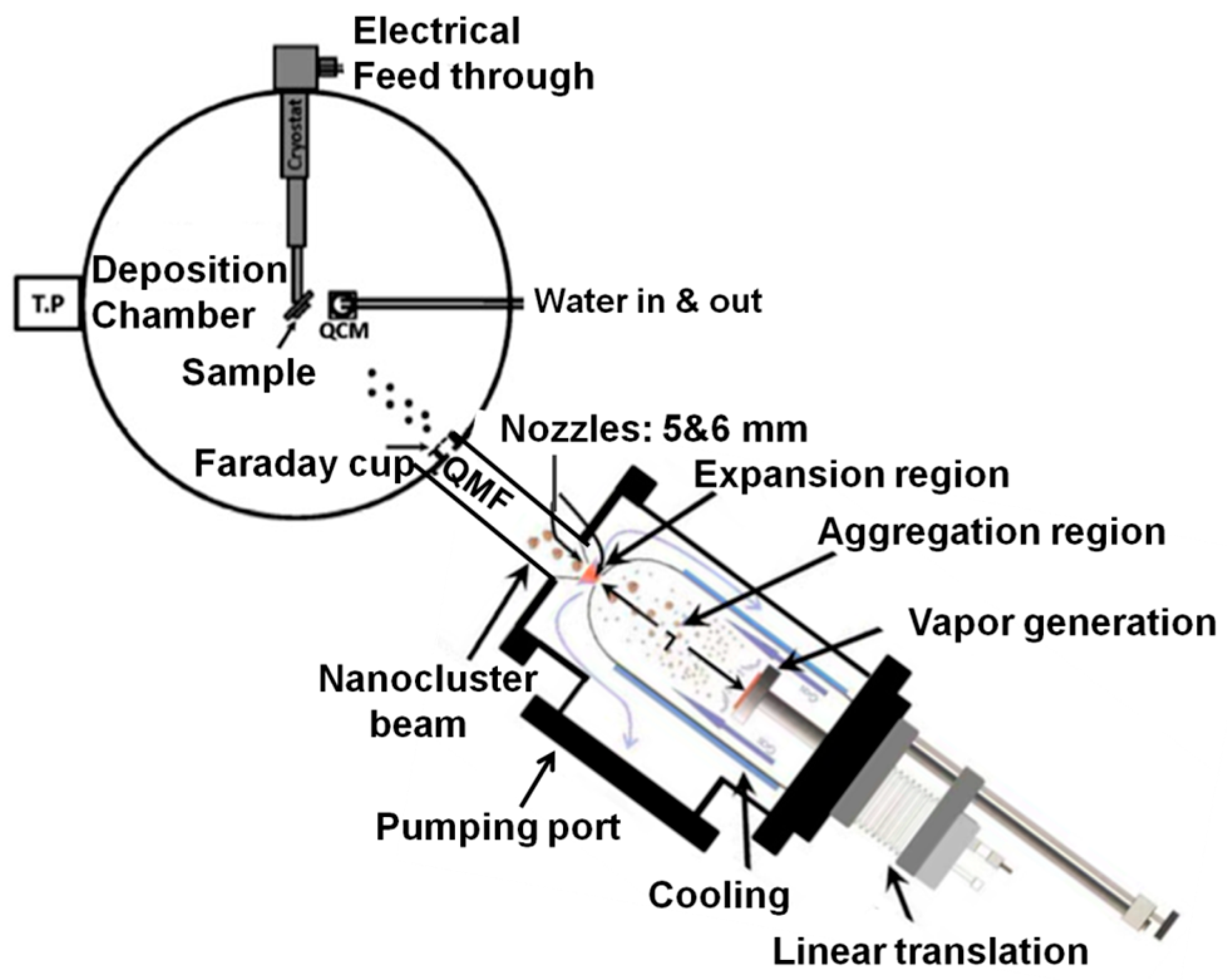
2. Materials and Methods

Aluminum nitride nanoparticles were fabricated by RF magnetron sputtering with inert gas condensation in the suitable system. We purchased the nanoparticles source from Mantis Deposition Ltd. (Oxfordshire, UK). A schematic diagram of the experimental research set-up in our lab for the fabrication of AlN nanoparticles is illustrated in Figure 1. The main parts of the system shown in this figure consist of a nanoparticle source that includes an RF magnetron sputtering unit, a turbo pump (TP), a quadrupolar mass filter (QMF), and the deposition chamber. The two turbo pumps were utilized to evacuate the main and source chambers to a base pressure of 10−8 mbar. The RF magnetron type discharge was used to generate nanoparticles from the AlN target purchased from the Kurt J. Lesker Company (Jefferson Hills, PA, USA) with a purity of 99.8%. Argon gas was used to create the plasma, sputter material from its target, establish nanoparticle condensation, and create pressure gradient between the source and deposition chambers that allowed nanoparticles to pass through the mass filter. In this research, the mass filter was used is a quadrupole mass filter located between the nanoparticle’s source and the deposition chamber.
The principle of QMF is based on applying alternating current AC and direct current DC voltages [±(U + Vcos ωt)] to four straight metal rods. The two rods were connected to a positive voltage while the other two rods to the negative voltage. Here, U is the DC voltage, V is the amplitude of AC voltage, ω is frequency, and t is time. Herein, a grid was placed at the outer part of the mass filter that was used to measure the ion flux of the selected mass/size, and the resulting current was measured by a pico-ampere-meter [18,19,20]. The Ar flow rate was fixed at 60 sccm which was controlled by a mass flow controller instrument MKS (Andover, MA, USA). Another part in the system was the magnetron gun placed in the source chamber which was mounted on a motorized linear translator that enables the aggregation length (L) to be varied up to 100 mm. In this experimental research, the aggregation length (L) was fixed at 30 mm and defined as the distance from the sputtering target surface to the source exit nozzle. The argon gas flow condensates the sputtered atoms to create the nanoparticles and sweeps the nanoparticles outside the source through the two nozzles into the main chamber. At this stage, the growth of nanoparticles stopped and they flowed through a quadrupole mass filter to measure the nanoparticle size distribution. The pressure gradient between the source and main chambers allowed the nanoparticles to flow and reach a substrate fixed where the nanoparticles were deposited on glass, mica, and silicon substrates. The size and shape of AlN nanoparticles were characterized by an atomic force microscope (AFM) provided by Dulcinea from Nanotec S.L. (Madrid, Spain). The X-ray diffraction analysis was obtained by using Shimadzu (Kyoto, Japan) 6100 XRD with CuΚα radiation (λ = 0.15406 nm). The energy dispersive spectroscopy (EDS, Jeol, Peabody, MA, USA) was used to measure the chemical composition. The optical absorption spectra were performed using Jasco UV-visible spectrophotometer (Tokyo, Japan). The Raman spectra were obtained using a Renishaw (Gloucestershire, UK) in Via Raman microscope with a laser excitation source working at wavelengths of 514 nm.

3. Results and Discussion

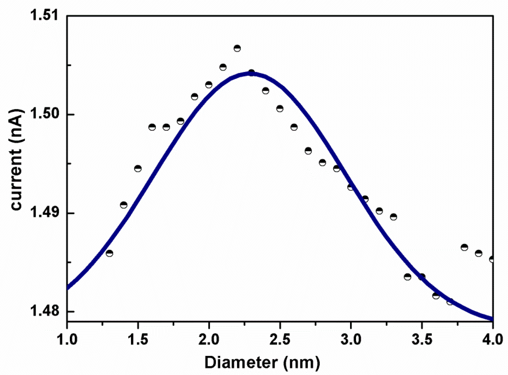
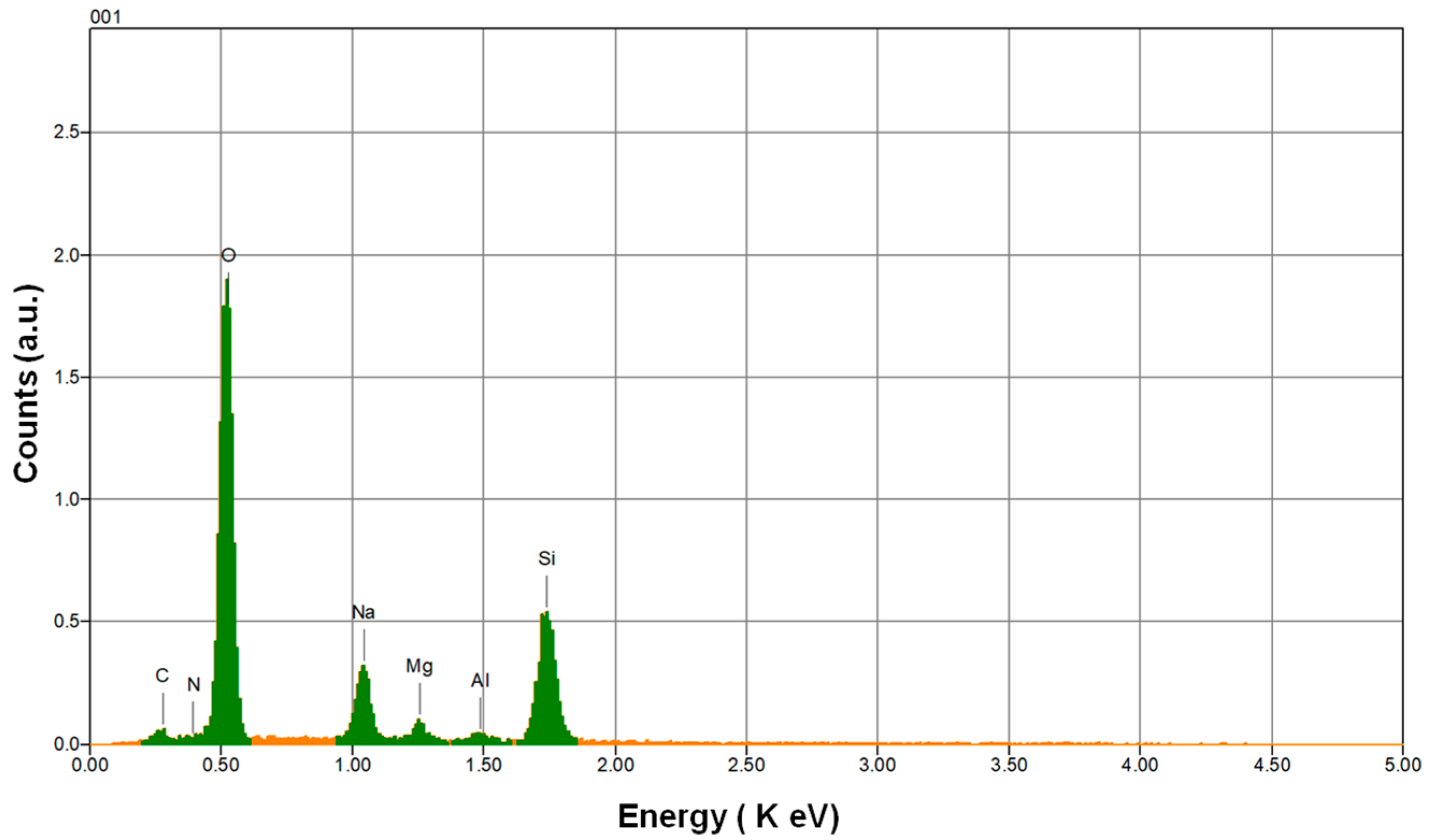
3.1. AFM, EDS, and XRD

The morphology, density, and height of AlN nanoparticles were determined by atomic force microscope topography images in a noncontact dynamic mode. Topography results possess high sensitivity due to the piezoelectric and tip characteristics. The AFM tip used was AR10-NCHR (Nano word) with a force constant of 42 N/m, resonance frequency of 320 kHz, and a tip radius of <15 nm. Figure 2a,b shows the AFM topographic image of AlN nanoparticles on the mica substrate. It is clear from the figure that the nanoparticles are spherical. The nanoparticles are presented as a three-dimensional projection in Figure 2c. The height analysis of these nanoparticles presented in Figure 2d shows that the apparent height ranged between 1.6 and 3 nm.
The Gaussian distribution presented by the solid line in Figure 3 is a fit for the sizes measured using the quadrupole mass filter of the nanoparticle’s production system. The Gaussian fit determines the size distribution of AlN nanoparticles, which were fabricated using a discharge power of 50 W, Argon flow rate (f = 60 sccm), chamber pressure P = 1.17 × 10⁻³ mbar, U/V = 0.09, and aggregation length (L = 30 mm). The figure shows that the peak diameter was about 2.5 nm. This result confirms the size distribution determined by the AFM shown in Figure 2d.
Figure 4 shows the element analysis of AlN nanoparticles determined by the electron dispersive spectroscopy EDS. The elemental atomic percentage in AlN nanoparticles was found to be Al = 0.62 and N = 0.67 which has Al/N ratio close to 1. Other elements indicated in Figure 4, such as oxygen, sodium, silicon, and carbon, arise from the glass substrate used for depositing the nanoparticles. Moreover, Table 1 shows element analysis determined by the EDS for the AlN nanoparticles on a glass substrate.
Figure 5 shows the XRD pattern of AlN nanoparticles deposited on the glass substrate. The diffraction peaks (002), (200), (103), and (311) are corresponding to the hexagonal phase structure reported in the literature [21,22,23,24].

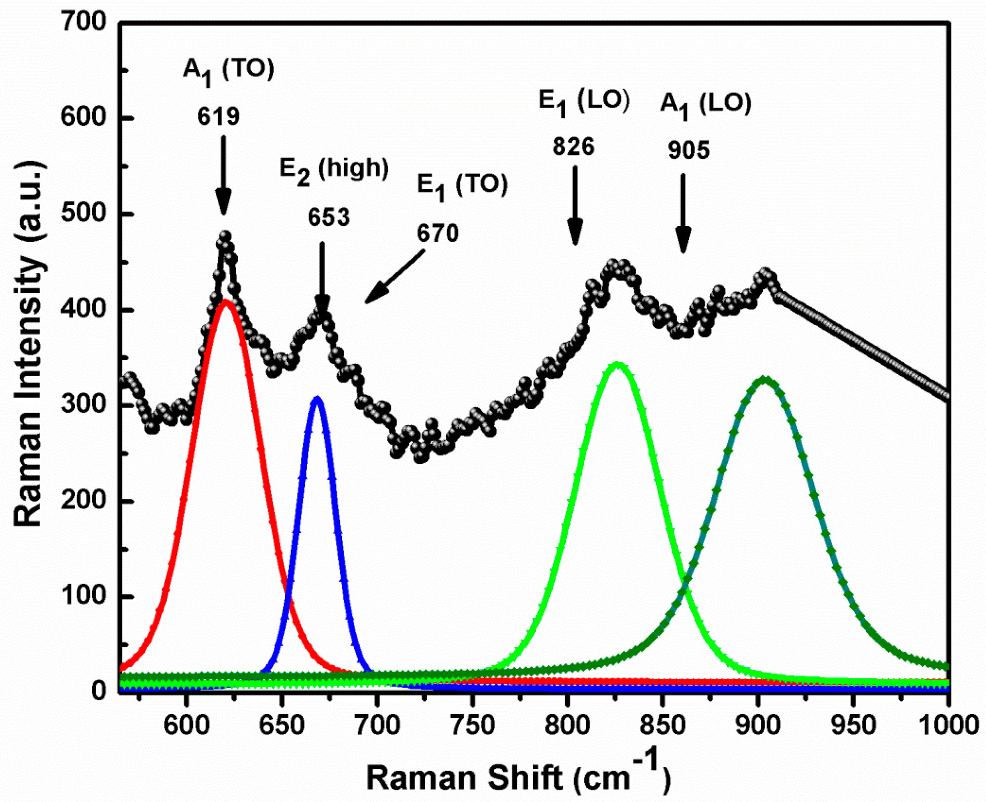
3.2. Raman Spectroscopy

To confirm the formation of the wurtzite structures of AlN nanoparticles, Raman spectroscopy was used. The space group of AlN is C 6 v 4 (P63mc) and the six Raman-active modes in AlN possibly determine as 1 A 1 ( TO ) + 1 A 1 ( LO ) + 1 E 1 ( TO ) + 1 E 1 ( LO ) + 2 E 2 [25]. Figure 6 illustrates the Raman spectra for AlN nanoparticles deposited on a silicon substrate. The Raman spectrum present in sold line was fitted by deconvolution of the Lorentzian line shape signal performed through a standard fitting procedure. Suitable fits are established with Lorentzian curves, whose centers are identified by the vibrational modes in the Raman spectrum. All the Raman modes were labeled with their corresponding values. The observed active Raman modes for AlN were found to be consistent with the wurtzite phase reported in the literature [26,27,28]. In this figure, the observed peak at 619 cm−1 corresponds to the transverse-optical A1(TO) mode, the broad beak centered at 670 cm−1 corresponds to E1(TO), and to the left of the maximum there is a hump with a lower intensity centered at 653 cm−1 corresponding to E2(high). In addition, the peaks at 826 and 905 cm−1 were assigned to longitudinal-optical E1(LO) and A1(LO), respectively. The Raman frequency shift peaks of AlN nanoparticles can slightly differ from their bulk that can be attributed to their crystallite sizes [29].

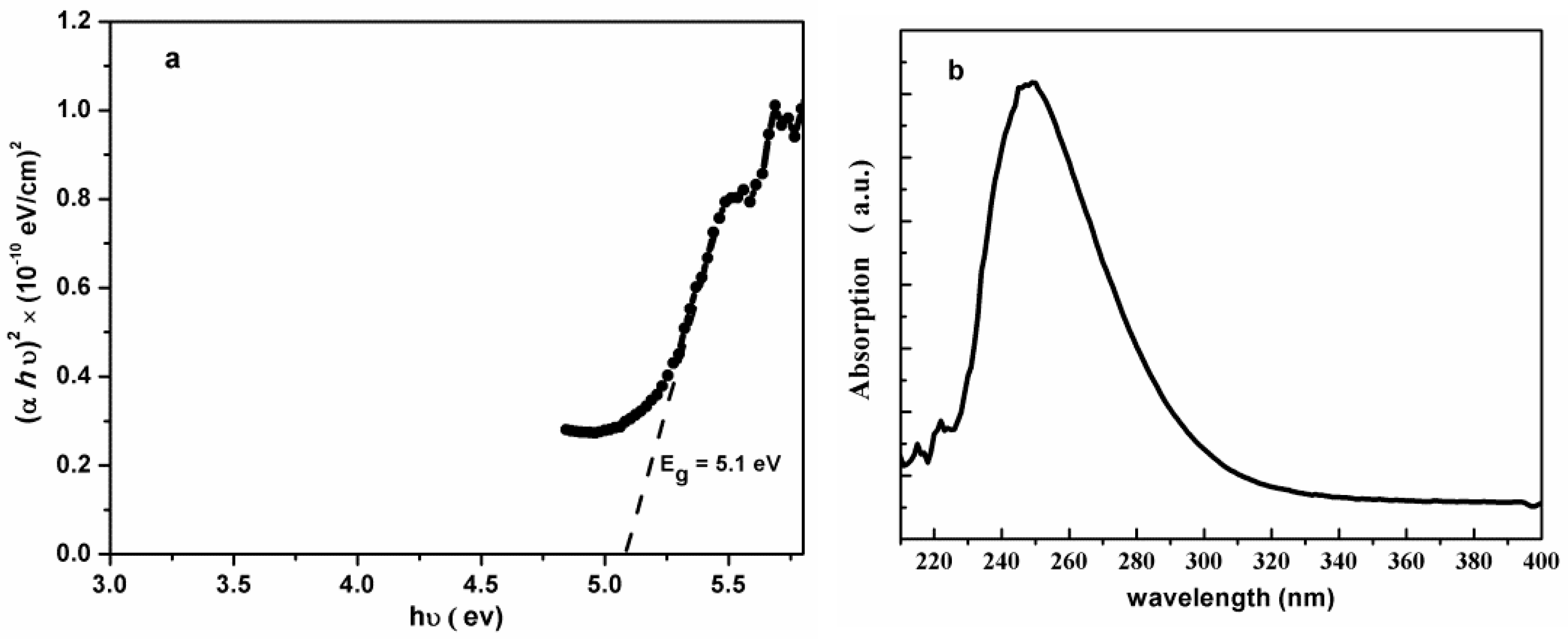
3.3. Optical Absorption

Optical information of AlN nanoparticles deposited on the glass substrate was determined by UV-visible spectroscopy. Figure 7 illustrates the Tauc plot [30], which is a graph for (αhν)2 versus the photon energy hν, where α is the optical absorption coefficient obtained from inset Figure 7. The optical energy gap (Eg) was determined by extrapolating the straight line that fit the linear portion of the Tauc plot the intercept the (hν)-axis at (αhν)2 = 0. The value obtained from this figure for AlN nanoparticles is equal to 5.1 eV. This value is in good agreement with the theoretical and experimental estimation reported in the literature [2,31,32].

4. Conclusions

Aluminum nitride nanoparticles were produced by a RF magnetron sputtering inert gas condensation technique inside an ultra-high vacuum system. The AFM images and quadrupole mass filter (QMF) indicated that the sizes of the nanoparticles were of the order of 3 nm. The X-ray diffraction studies confirmed the wurtzite phase of AlN nanoparticles. Furthermore, Raman spectroscopy measurements showed vibration transverse-optical modes and longitudinal-optical modes. The broadening peaks of the Raman vibrational modes were due to the nano-size effects. Moreover, the optical bandgap energy obtained for AlN nanoparticles was 5.1 eV. It is worth noting that the production of AlN nanostructures has a potential to be used in fabrication nanoscale devices.

Author Contributions

Conceptualization, I.M. and N.Q.; methodology, I.M., N.Q., K.S. and H.A.; validation, I.M., N.Q. and S.T.M.; data curation, I.M., N.Q. and S.T.M.; writing—original draft preparation, I.M.; writing—review and editing, I.M. and N.Q. All authors have read and agreed to the published version of the manuscript.

Funding

This research was funded by United Arab Emirates University under UPAR grants number 31S207 and 31S313.

Conflicts of Interest

The authors declare no conflict of interest.

References

  1. Litimein, F.; Bouhafs, B.; Dridi, Z.; Ruterana, P. The electronic structure of wurtzite and zincblende AlN: An ab initio comparative study. New J. Phys. 2002, 4, 64. [Google Scholar] [CrossRef] [Green Version]
  2. Choudhary, R.K.; Mishra, P.; Biswas, A.; Bidaye, A.C. Structural and optical properties of aluminum nitride thin films deposited by pulsed DC magnetron sputtering. Int. Sch. Res. Not. 2013, 2013, e759462. [Google Scholar] [CrossRef]
  3. Yong, K.-T.; Yu, S.F. AlN nanowires: Synthesis, physical properties, and nanoelectronics applications. J. Mater. Sci. 2012, 47, 5341–5360. [Google Scholar]
  4. Kumari, N.; Singh, A.K.; Barhai, P.K. Study of properties of AlN thin films deposited by reactive magnetron sputtering. Int. J. Thin Film. Sci. Technol. 2014, 3, 43–49. [Google Scholar] [CrossRef]
  5. Dutheil, P.; Orlianges, J.-C.; Crunteanu, A.; Catherinot, A.; Champeaux, C. AlN, ZnO thin films and AlN/ZnO or ZnO/AlN multilayer structures deposited by PLD for surface acoustic wave applications: Deposited AlN, ZnO thin films and AlN/ZnO or ZnO/AlN multilayer structures. Phys. Status Solidi (a) 2015, 212, 817–825. [Google Scholar] [CrossRef]
  6. Zhao, S.; Connie, A.T.; Dastjerdi, M.H.T.; Kong, X.H.; Wang, Q.; Djavid, M.; Sadaf, S.; Liu, X.D.; Shih, I.; Guo, H.; et al. Aluminum nitride nanowire light emitting diodes: Breaking the fundamental bottleneck of deep ultraviolet light sources. Sci. Rep. 2015, 5, 8332. [Google Scholar] [CrossRef] [PubMed]
  7. Tran, B.T.; Hirayama, H. Growth and fabrication of high external quantum efficiency AlGaN-based deep ultraviolet light-emitting diode grown on pattern Si substrate. Sci. Rep. 2017, 7, 1–6. [Google Scholar] [CrossRef]
  8. Aluminum Nitride (AlN) Substrates LED. Available online: http://www.crystal-n.com/Applications/led.html (accessed on 12 May 2015).
  9. Taniyasu, Y.; Kasu, M.; Makimoto, T. Aluminum nitride deep-ultraviolet light-emitting diodes. NTT Tech. Rev. 2006, 4, 5. [Google Scholar]
  10. Tang, Y.B.; Cong, H.T.; Zhao, Z.G.; Cheng, H.M. Field emission from AlN nanorod array. Appl. Phys. Lett. 2005, 86, 153104. [Google Scholar] [CrossRef]
  11. Zheng, J.; Song, X.; Zhang, Y.; Li, Y.; Li, X.; Pu, Y. Nanosized aluminum nitride hollow spheres formed through a self-templating solid–gas interface reaction. J. Solid State Chem. 2007, 180, 276–283. [Google Scholar] [CrossRef]
  12. Zhang, Y.; Liu, J.; He, R.; Zhang, Q.; Zhang, X.; Zhu, J. Synthesis of aluminum nitride nanowires from carbon nanotubes. Chem. Mater. 2001, 13, 3899–3905. [Google Scholar] [CrossRef]
  13. Vispute, R.D.; Wu, H.; Narayan, J. High quality epitaxial aluminum nitride layers on sapphire by pulsed laser deposition. Appl. Phys. Lett. 1995, 67, 1549–1551. [Google Scholar] [CrossRef]
  14. Hong, S.-U.; Paek, M.-C.; Han, G.-P.; Sohn, Y.-J.; Kim, T.-Y.; Cho, K.-I.; Shim, K.-H.; Yoon, S.-G. Characterization of aluminum nitride thin films on silicon substrates grown by plasma assisted molecular beam epitaxy. Jpn. J. Appl. Phys. 2002, 41, 5507. [Google Scholar] [CrossRef]
  15. Iqbal, A.; Mohd-Yasin, F. Reactive sputtering of aluminum nitride (002) thin films for piezoelectric applications: A review. Sensors 2018, 18, 1797. [Google Scholar] [CrossRef] [Green Version]
  16. Rani, A.; Reddy, R.; Sharma, U.; Mukherjee, P.; Mishra, P.; Kuila, A.; Sim, L.C.; Saravanan, P. A review on the progress of nanostructure materials for energy harnessing and environmental remediation. J. Nanostruct. Chem. 2018, 8, 255–291. [Google Scholar] [CrossRef] [Green Version]
  17. Ouldhamadouche, N.; Achour, A.; Musa, I.; Ait Aissa, K.; Massuyeau, F.; Jouan, P.Y.; Kechouane, M.; Le Brizoual, L.; Faulques, E.; Barreau, N.; et al. Structural and photoluminescence characterization of vertically aligned multiwalled carbon nanotubes coated with ZnO by magnetron sputtering. Thin Solid Film. 2012, 520, 4816–4819. [Google Scholar] [CrossRef]
  18. Ayesh, A.I.; Thaker, S.; Qamhieh, N.; Ghamlouche, H. Size-controlled Pd nanocluster grown by plasma gas-condensation method. J. Nanopart. Res. 2011, 13, 1125–1131. [Google Scholar] [CrossRef]
  19. Ayesh, A.I.; Qamhieh, N.; Ghamlouche, H.; Thaker, S.; El-Shaer, M. Fabrication of size-selected Pd nanoclusters using a magnetron plasma sputtering source. J. Appl. Phys. 2010, 107, 034317. [Google Scholar] [CrossRef]
  20. Ayesh, A.I. Size-selected fabrication of alloy nanoclusters by plasma-gas condensation. J. Alloys Compd. 2018, 745, 299–305. [Google Scholar] [CrossRef]
  21. Balasubramanian, C.; Bellucci, S.; Cinque, G.; Marcelli, A.; Guidi, M.C.; Piccinini, M.; Popov, A.; Soldatov, A.; Onorato, P. Characterization of aluminium nitride nanostructures by XANES and FTIR spectroscopies with synchrotron radiation. J. Phys. Condens. Matter 2006, 18, S2095–S2104. [Google Scholar] [CrossRef]
  22. Gao, Z.; Wan, Y.; Xiong, G.; Guo, R.; Luo, H. Synthesis of aluminum nitride nanoparticles by a facile urea glass route and influence of urea/metal molar ratio. Appl. Surf. Sci. 2013, 280, 42–49. [Google Scholar] [CrossRef]
  23. Shi, Z.; Radwan, M.; Kirihara, S.; Miyamoto, Y.; Jin, Z. Combustion synthesis of rod-like AlN nanoparticles. J. Ceram. Soc. Jpn. 2008, 116, 975–979. [Google Scholar] [CrossRef] [Green Version]
  24. Panda, P.; Mishra, G.; Mantry, S.; Singh, S.K.; Sinha, S.P. A study on mechanical, thermal, and electrical properties of glass fiber-reinforced epoxy hybrid composites filled with plasma-synthesized AlN. J. Compos. Mater. 2014, 48, 3073–3082. [Google Scholar] [CrossRef]
  25. Cao, Y.G.; Chen, X.L.; Lan, Y.C.; Li, J.Y.; Xu, Y.P.; Xu, T.; Liu, Q.L.; Liang, J.K. Blue emission and Raman scattering spectrum from AlN nanocrystalline powders. J. Cryst. Growth 2000, 213, 198–202. [Google Scholar] [CrossRef]
  26. Liu, M.S.; Nugent, K.W.; Prawer, S.; Bursill, L.A.; Peng, J.L.; Tong, Y.Z.; Jewsbury, P. Micro-Raman Scattering Properties of Highly Oriented AlN Films. Int. J. Mod. Phys. B 1998, 12, 1963–1974. [Google Scholar] [CrossRef]
  27. Kuball, M.; Hayes, J.M.; Prins, A.D.; van Uden, N.W.A.; Dunstan, D.J.; Shi, Y.; Edgar, J.H. Raman scattering studies on single-crystalline bulk AlN under high pressures. Appl. Phys. Lett. 2001, 78, 724–726. [Google Scholar] [CrossRef]
  28. Shen, L.; Cheng, T.; Wu, L.; Li, X.; Cui, Q. Synthesis and optical properties of aluminum nitride nanowires prepared by arc discharge method. J. Alloys Compd. 2008, 465, 562–566. [Google Scholar] [CrossRef]
  29. Qadri, S.B.; Gorzkowski, E.P.; Rath, B.B.; Feng, C.R.; Amarasinghe, R. Nanoparticles of wurtzite aluminum nitride from the nut shells. AIP Adv. 2016, 6, 115204. [Google Scholar] [CrossRef] [Green Version]
  30. Musa, I.; Qamhieh, N.; Mahmoud, S.T. Synthesis and length dependent photoluminescence property of zinc oxide nanorods. Results Phys. 2017, 7, 3552–3556. [Google Scholar] [CrossRef]
  31. Yim, W.M.; Stofko, E.J.; Zanzucchi, P.J.; Pankove, J.I. Epitaxially grown AlN and its optical band gap. J. Appl. Phys. 1973, 44, 6. [Google Scholar] [CrossRef]
  32. Badylevich, M.; Shamuilia, S.; Afanas’ev, V.V.; Stesmans, A.; Fedorenko, Y.G.; Zhao, C. Electronic structure of the interface of aluminum nitride with Si(100). J. Appl. Phys. 2008, 104, 093713. [Google Scholar] [CrossRef]
Figure 1. Schematic diagram of the deposition system, including the nanoparticle source and deposition chamber [18].
Coatings 10 00411 g001
Figure 2. Atomic force microscopy (AFM) topography images of aluminum nitride (AlN) nanoparticles on a mica substrate. Scan sizes of (a) 2.5 μm × 2.5 μm and (b) 1.5 μm × 1.5 μm. (c) Three-dimensional projection of nanoparticles and (d) line profiles for the 2 separate nanoparticles identified in the image (b). The deposition time while using quadrupol mass filter (QMF) is 4 h.
Coatings 10 00411 g002
Figure 3. The Gaussian fit data solid line is the size distribution of AlN nanoparticles using a quadrupole mass filter.
Coatings 10 00411 g003
Figure 4. EDS spectrum of AlN nanoparticles deposited on the glass substrate.
Coatings 10 00411 g004
Figure 5. XRD spectrum of the AlN nanoparticles deposited on the glass substrate.
Coatings 10 00411 g005
Figure 6. Raman spectra of AlN nanoparticles deposited on the silicon substrate.
Coatings 10 00411 g006
Figure 7. (a) Tauc plot of bandgap energy for AlN nanoparticles deposited on the glass substrate. (b) Absorption of AlN nanoparticles deposited on glass substrate.
Coatings 10 00411 g007
Table 1. Element analysis determined by the EDS for the AlN nanoparticles on the glass substrate.
FormulaMass%Atom%SigmaNetK Ratio Line
N0.510.670.131090.0004177K
Al0.920.620.089130.0013102K

