Theoretical and Experimental Study of Particle Distribution from Magnetron Sputtering with Masks for Accurate Thickness Profile Control


Abstract
1. Introduction
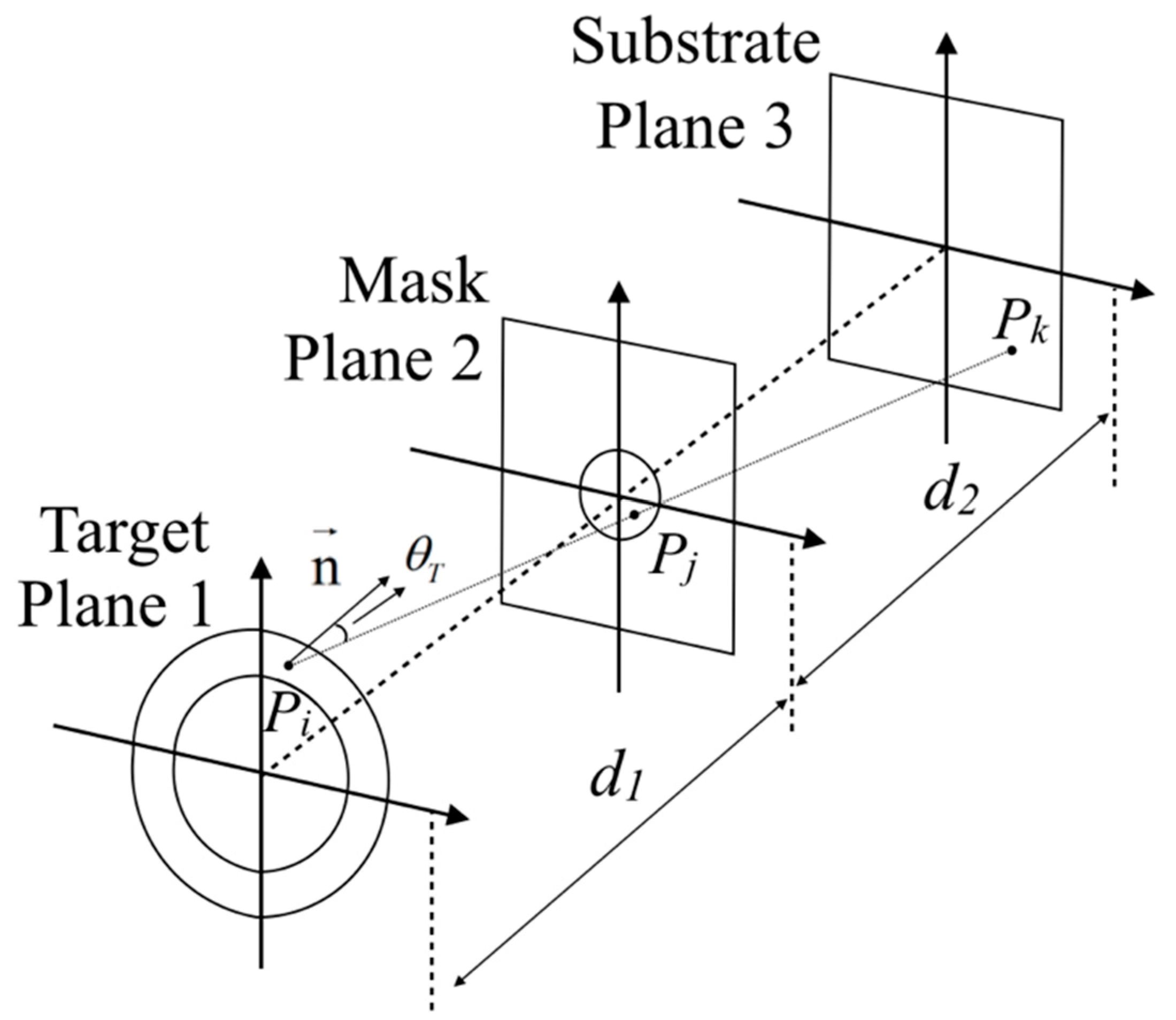
2. Modeling
2.1. Positional Probability of Particles Sputtered out of the Circular Target
2.2. Angular Distribution of the Sputtered Particles
2.3. Straight Line Transport of Sputtered Particles Passing through the Mask
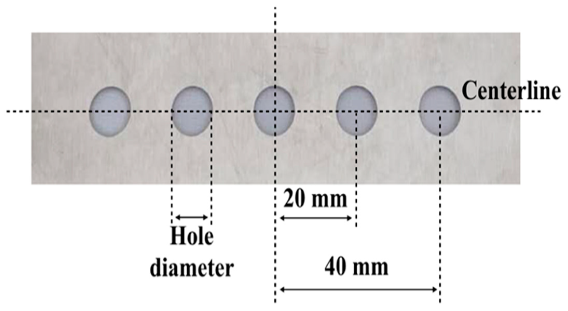
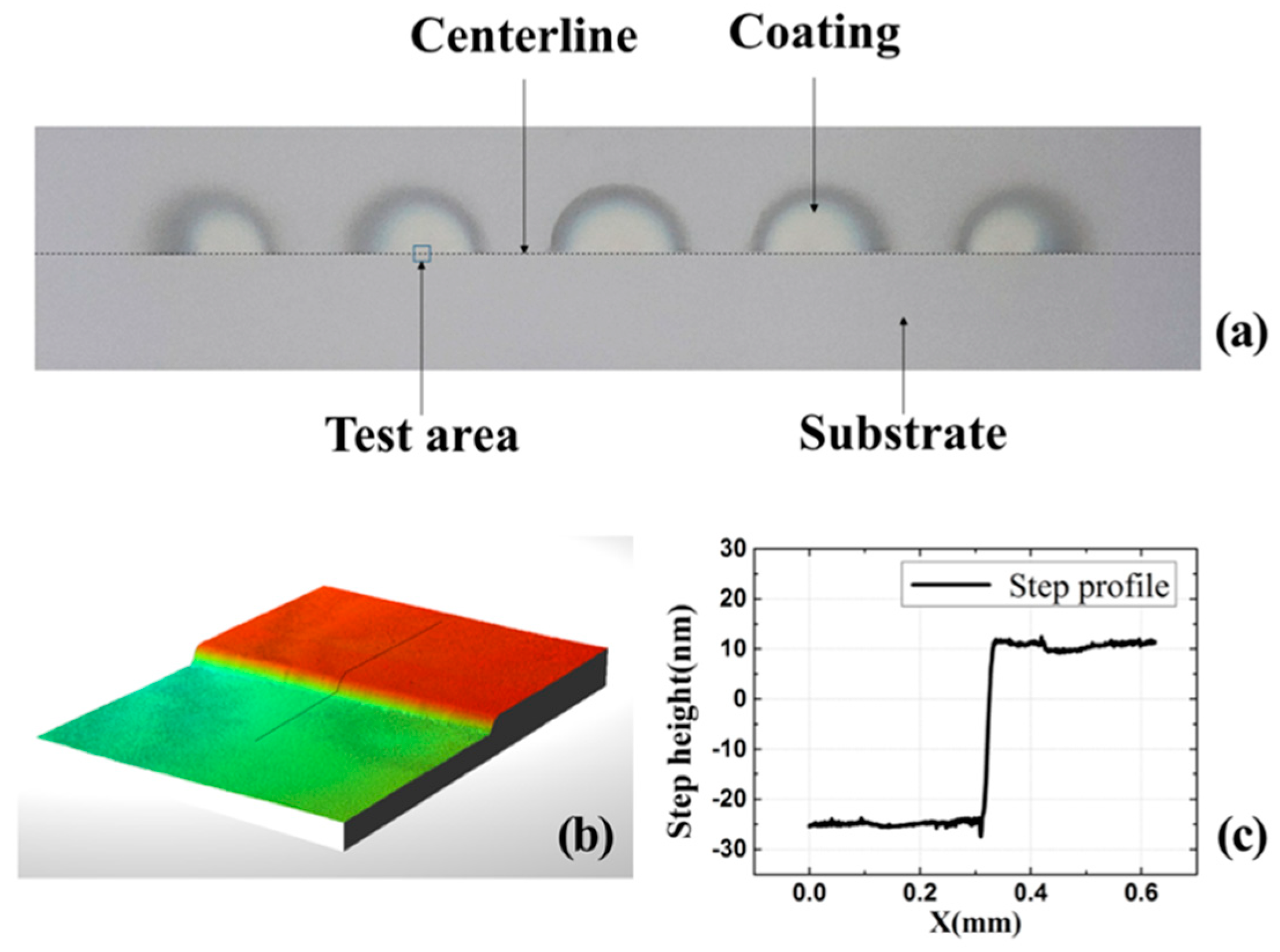
3. Experiments
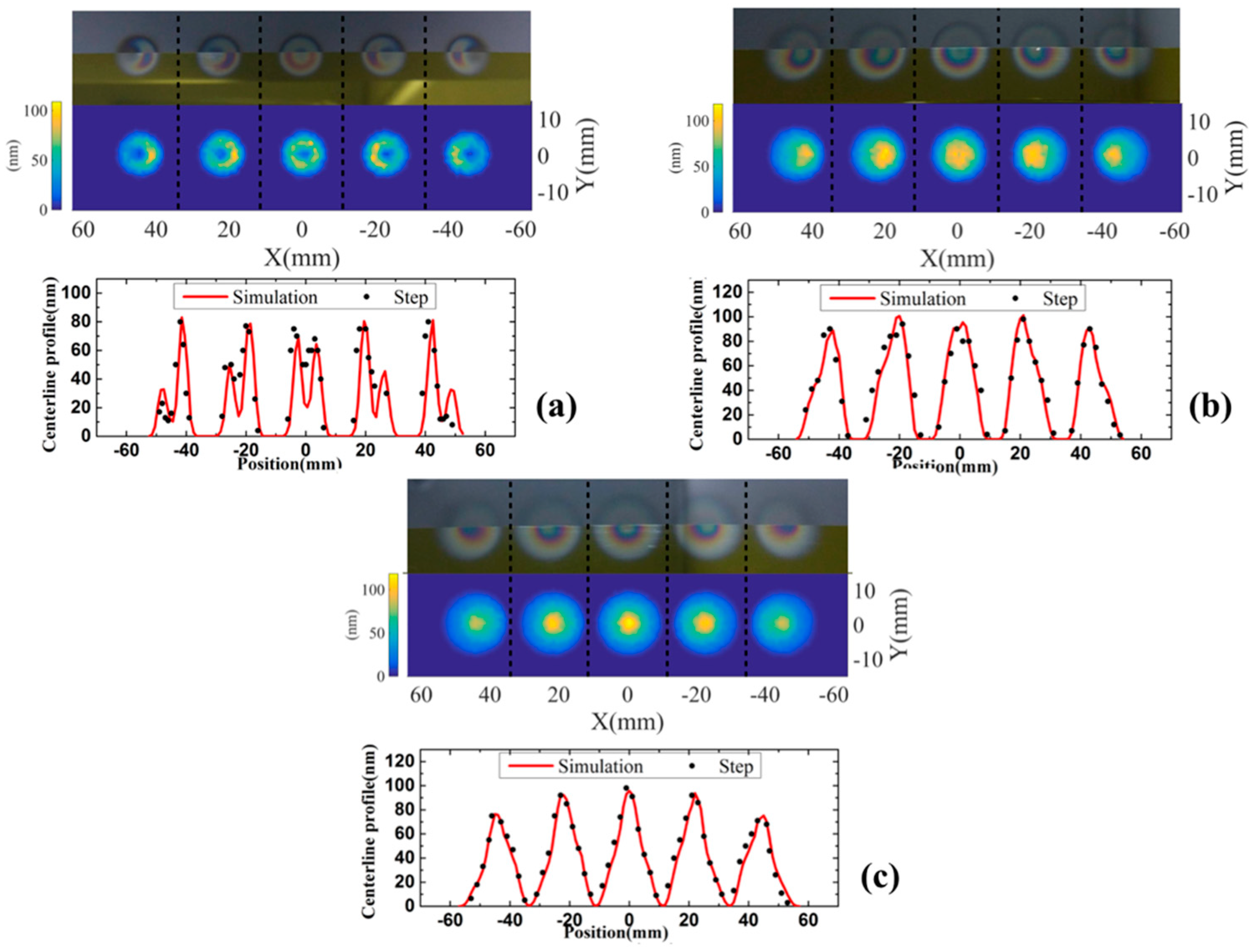
4. Experimental Results and Discussion
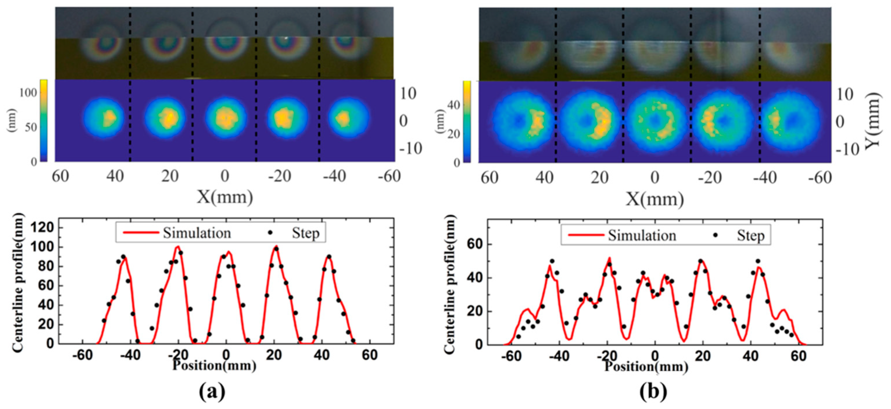
4.1. Comparison of Different Hole Sizes on the Masks
4.2. Comparison of Different Distances of the Mask between the Target and the Substrate
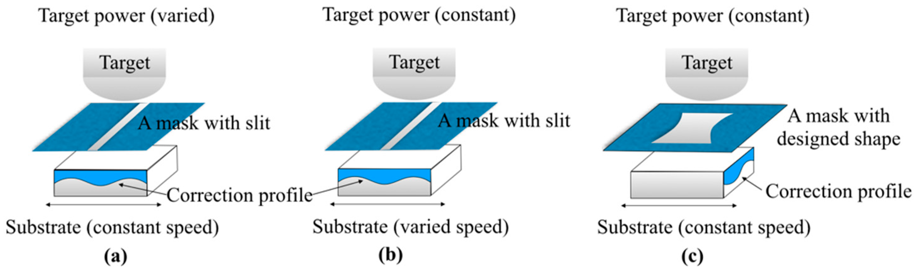
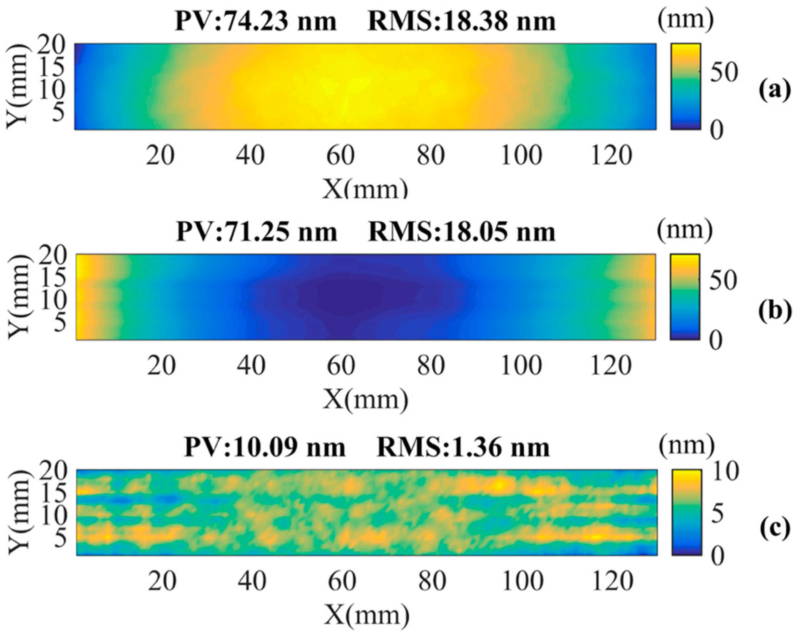
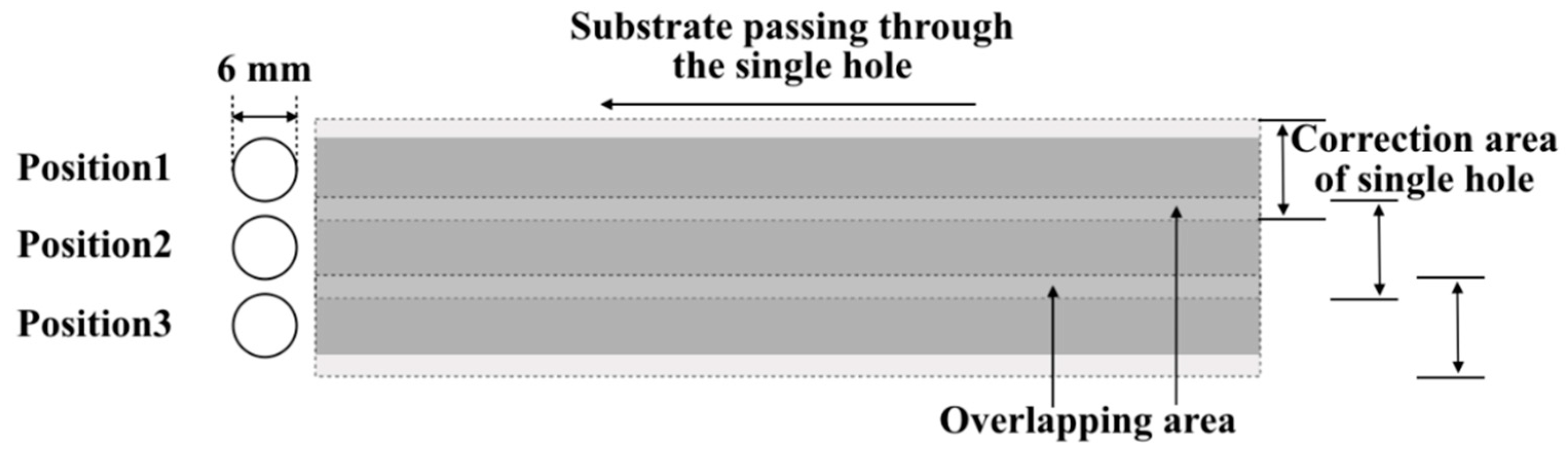
4.3. Applications of the Established Model
5. Conclusions
Author Contributions
Funding
Conflicts of Interest
References
- Mori, Y.; Yamauchi, Y.; Yamamura, K.; Mimura, H.; Saito, A.; Kishimoto, H.; Sekito, Y.; Kanaoka, M.; Souvorov, A.; Yabashi, M.; et al. Development of plasma chemical vaporization machining and elastic emission machining systems for coherent x-ray optics. In Proceedings of the X-Ray Mirrors, Crystals, and Multilayers, San Diego, CA, USA, 30–31 July 2001; pp. 30–42. [Google Scholar]
- Yamauchi, K.; Mimura, H.; Inagaki, K.; Mori, Y. Figuring with subnanometer-level accuracy by numerically controlled elastic emission machining. Rev. Sci. Instrum. 2002, 73, 4028–4033. [Google Scholar] [CrossRef]
- Kubota, A.; Shinbayashi, Y.; Mimura, H.; Sano, Y.; Inagaki, K.; Mori, Y.; Yamauchi, K. Investigation of the surface removal process of silicon carbide in elastic emission machining. J. Electron. Mater. 2007, 36, 92–97. [Google Scholar] [CrossRef]
- Yuan, Z.; Dai, Y.F.; Xie, X.H.; Zhou, L. Ion Beam Figuring System for Ultra-Precise Optics. Key Eng. Mater. 2012, 516, 19–24. [Google Scholar] [CrossRef]
- Peverini, L.; Kozhevnikov, I.V.; Rommeveaux, A.; Vaerenbergh, P.V.; Claustre, L.; Guillet, S.; Massonnat, J.Y.; Ziegler, E.; Susini, J. Ion beam profiling of aspherical X-ray mirrors. Nucl. Instrum. Methods Phys. Res. A 2010, 616, 115–118. [Google Scholar] [CrossRef]
- Idir, M.; Lei, H.; Bouet, N.; Kaznatcheev, K.; Vescovi, M.; Lauer, K.; Conley, R.; Rennie, K.; Kahn, J.; Nethery, R.; et al. A one-dimensional ion beam figuring system for X-ray mirror fabrication. Rev. Sci. Instrum. 2015, 86, 105120. [Google Scholar] [CrossRef]
- Mimura, H.; Yumoto, H.; Matsuyama, S.; Yamamura, K.; Sano, Y.; Ueno, K.; Endo, K.; Mori, Y.; Yabashi, M.; Tamasaku, K.; et al. Relative angle determinable stitching interferometry for hard x-ray reflective optics. Rev. Sci. Instrum. 2005, 76, 045102. [Google Scholar] [CrossRef]
- Thiess, H.; Lasser, H.; Siewert, F. Fabrication of X-ray mirrors for synchrotron applications. Nucl. Instrum. Methods Phys. Res. A 2010, 616, 157–161. [Google Scholar] [CrossRef]
- Handa, S.; Mimura, H.; Yumoto, H.; Kimura, T.; Matsuyama, S.; Sano, Y.; Yamauchi, K. Highly accurate differential deposition for X-ray reflective optics. Surf. Interface Anal. 2008, 40, 1019–1022. [Google Scholar] [CrossRef]
- Alcock, S.G.; Cockerton, S. A preferential coating technique for fabricating large, high quality optics. Nucl. Instrum. Methods Phys. Res. A 2010, 616, 110–114. [Google Scholar] [CrossRef]
- Kilaru, K.; Ramsey, B.D.; Gubarev, M.V. Development of differential deposition technique for figure corrections in grazing incidence X-ray optics. In Proceedings of the Optics for EUV, X-Ray, and Gamma-Ray Astronomy IV, San Diego, CA, USA, 4 August 2009; p. 743719. [Google Scholar]
- Kilaru, K.; Ramsey, B.D.; Kolodziejczak, J.; Atkins, C. Improving x-ray optics via differential deposition. In Proceedings of the Optics for EUV, X-Ray and Gamma-Ray Astronomy VIII, San Diego, CA, USA, 8–10 August 2017; p. 103991F. [Google Scholar]
- Ice, G.E.; Chung, J.-S.; Tischler, J.Z.; Lunt, A.; Assoufid, L. Elliptical x-ray microprobe mirrors by differential deposition. Rev. Sci. Instrum. 2000, 71, 2635–2639. [Google Scholar] [CrossRef]
- Liu, C.; Conley, R.; Assoufid, L.; Cai, Z.; Qian, J.; Macrander, A.T. From Flat Substrate to Elliptical KB Mirror by Profile Coating. In Proceedings of the 8th International Conference on Synchrotron Radiation Instrumentation, San Francisco, CA, USA, 25–29 August 2003; pp. 704–707. [Google Scholar]
- Bing, S.; Chian, L.; Jun, Q.; Wenjun, L.; Assoufid, L.; Khounsary, A.; Conley, R.; Macrander, A.T. Platinum Kirkpatrik-Baez mirrors for a hard x-ray microfocusing system made by profile coating. In Proceedings of the Advances in X-Ray/EUV Optics and Components V, San Diego, CA, USA, 2–3 August 2010; p. 78020G. [Google Scholar]
- Liu, C.; Assoufid, L.; Conley, R.; Macrander, A.T.; Ice, G.E.; Tischler, J.Z. Profile coating and its application for Kirkpatrick-Baez mirrors. Opt. Eng. 2003, 42, 3622–3628. [Google Scholar] [CrossRef]
- Liu, C.; Conley, R.; Macrander, A.T. Functional profile coatings and film stress. J. Vac. Sci. Technol. 2004, 22, 1610–1614. [Google Scholar] [CrossRef]
- Zhang, Z.; Qi, R.Z.; Yao, Y.Y.; Shi, Y.N.; Li, W.B.; Huang, Q.S.; Yi, S.Z.; Zhang, Z.; Wang, Z.S.; Xie, C. Improving Thickness Uniformity of Mo/Si Multilayers on Curved Spherical Substrates by a Masking Technique. Coatings 2019, 9, 851. [Google Scholar] [CrossRef]
- Yingna, S.; Runze, Q.; Yufei, F.; Qiushi, H.; Zhengxiang, S.; Zhanshan, W. Microstructure, roughness, and stress properties of silicon coatings for shape correction of Kirkpatrick-Baez mirrors. Opt. Eng. 2019, 58, 015103. [Google Scholar] [CrossRef]
- Lizhen, Z.; Enze, W.; Zhengquan, Z.; Lige, W.; Yongsheng, Z.; Shaowu, C.; Xiaoan, Y. Study on new technology of removing abandoned tobacco zinc plate coating by using mechanical method. Adv. Mater. Res. 2012, 472–475, 2944–2947. [Google Scholar] [CrossRef]
- Mizuno, K.; Habuka, H.; Ishida, Y.; Ohno, T. In Situ Cleaning Process of Silicon Carbide Epitaxial Reactor for Removing Film-Type Deposition Formed on Susceptor. Mater. Sci. Forum 2016, 858, 237–240. [Google Scholar] [CrossRef]
- Pa, P.S. A removing process for multilayer nano thin-film structures on the hard disk surface. Int. J. Adv. Manuf. Technol. 2014, 70, 459–467. [Google Scholar] [CrossRef]
- Zubar, T.I.; Fedosyuk, V.M.; Trukhanov, A.V.; Kovaleva, N.N.; Astapovich, K.A.; Vinnik, D.A.; Trukhanova, E.L.; Kozlovskiy, A.L.; Zdorovets, M.V.; Solobai, A.A.; et al. Control of growth mechanism of electrodeposited nanocrystalline NiFe films. J. Electrochem. Soc. 2019, 166, D173–D180. [Google Scholar] [CrossRef]
- Warcholinski, B.; Gilewicz, A.; Lupicka, O.; Kuprin, A.S.; Tolmachova, G.N.; Ovcharenko, V.D.; Kolodiy, I.V.; Sawczak, M.; Kochmanska, A.E.; Kochmanski, P.; et al. Structure of CrON coatings formed in vacuum arc plasma fluxes. Surf. Coat. Technol. 2017, 309, 920–930. [Google Scholar] [CrossRef]
- Zavaleyev, V.; Walkowicz, J.; Kuznetsova, T.; Zubar, T. The dependence of the structure and mechanical properties of thin ta-C coatings deposited using electromagnetic venetian blind plasma filter on their thickness. Thin Solid Films 2017, 638, 153–158. [Google Scholar] [CrossRef]
- Broadway, D.M.; Platonov, Y.Y.; Gomez, L.A. Achieving desired thickness gradients on flat and curved substrates. In Proceedings of the 1999 X-Ray Optics, Instruments, and Missions II, Denver, CO, USA, 18–20 July 1999; pp. 262–274. [Google Scholar]
- Mahieu, S.; Buyle, G.; Depla, D.; Heirwegh, S.; Ghekiere, P.; De Gryse, R. Monte Carlo simulation of the transport of atoms in DC magnetron sputtering. Nucl. Instrum. Methods Phys. Res. B 2006, 243, 313–319. [Google Scholar] [CrossRef]
- Yamazaki, T.; Matsuda, K.; Nakatani, H. Effect of angular distribution of ejected atoms from a target on the uniformity of thickness and composition of MoSix sputtering films. Jpn. J. Appl. Phys. 1990, 29, 1304–1309. [Google Scholar] [CrossRef]
- Ekpe, S.D.; Bezuidenhout, L.W.; Dew, S.K. Deposition rate model of magnetron sputtered particles. Thin Solid Films 2005, 474, 330–336. [Google Scholar] [CrossRef]
- Zhang, J.; Wang, Z.; Tao, Z.; Pan, J. The angular distributions of sputtered indium atoms at different temperature. J. Mater. Sci. Lett. 1993, 12, 747–748. [Google Scholar] [CrossRef]
- Andersen, H.H.; Stenum, B.; Sorensen, T.; Whitlow, H.J. Angular distribution of particles sputtered from Cu, Pt, and Ge targets by keV Ar+ ion bombardment. Nucl. Instrum. Methods Phys. Res. B 1985, B6, 459–465. [Google Scholar] [CrossRef]
- Chang-Gyu, K.; Won-Jong, L. An angular distribution function for the sputter-depositing atoms and general equations describing the initial thickness profile of a thin film deposited inside a via and trench by sputtering. Thin Solid Films 2010, 519, 74–80. [Google Scholar] [CrossRef]
- Escrivao, M.L.; Pereira, P.J.S.; Ferreira, J.L.; Teixeira, M.R.; Maneira, M.J.P. Argon temperature and density versus the input power in a high pressure planar magnetron discharge. Vacuum 2002, 64, 367–371. [Google Scholar] [CrossRef]
- Westwood, W.D. Calculation of deposition rates in diode sputtering systems. J. Vac. Sci. Technol. 1978, 15, 1–9. [Google Scholar] [CrossRef]
- Chang, S.A.; Skolnik, M.B.; Altman, C. High rate sputtering deposition of nickel using Dc magnetron mode. J. Vac. Sci. Technol. A 1986, 4, 413–416. [Google Scholar] [CrossRef]
- Ozimek, M.; Wilczynski, W.; Szubzda, B. Magnetic thin film deposition with pulsed magnetron sputtering: Deposition rate and film thickness distribution. In Proceedings of the 8th National Scientific Conference Advances in Electrotechnology, Jamrozowa Polana, Poland, 23–25 September 2015; p. 012009. [Google Scholar]
- Ma, S.; Shen, Z.; Chen, S.; Wang, Z. Fractal surface for calibration of an optical profiler. Optik 2014, 125, 4685–4688. [Google Scholar] [CrossRef]
- Zhang, X.; Zeng, X.; Hu, H.; Luo, X. Manufacturing and testing large SiC mirrors in an efficient way. In Proceedings of the Optical Systems Design 2015: Optical Fabrication, Testing and Metrology V, Jena, Germany, 7 September 2015; p. 96280S. [Google Scholar]


| Variables | Target–Substrate Distance (mm) | d1 (mm) | d2 (mm) | Hole Diameter (mm) | Deposition Time (s) |
|---|---|---|---|---|---|
| Hole size | 70 | 62 | 8 | 3 | 5400 |
| 70 | 62 | 8 | 6 | 2100 | |
| 70 | 62 | 8 | 10 | 900 | |
| Mask distance | 70 | 62 | 8 | 6 | 2100 |
| 70 | 57 | 13 | 6 | 2100 |
© 2020 by the authors. Licensee MDPI, Basel, Switzerland. This article is an open access article distributed under the terms and conditions of the Creative Commons Attribution (CC BY) license (http://creativecommons.org/licenses/by/4.0/).
Share and Cite
Shi, Y.; Huang, Q.; Qi, R.; Shen, Z.; Zhang, Z.; Wang, Z. Theoretical and Experimental Study of Particle Distribution from Magnetron Sputtering with Masks for Accurate Thickness Profile Control. Coatings 2020, 10, 357. https://doi.org/10.3390/coatings10040357
Shi Y, Huang Q, Qi R, Shen Z, Zhang Z, Wang Z. Theoretical and Experimental Study of Particle Distribution from Magnetron Sputtering with Masks for Accurate Thickness Profile Control. Coatings. 2020; 10(4):357. https://doi.org/10.3390/coatings10040357
Chicago/Turabian StyleShi, Yingna, Qiushi Huang, Runze Qi, Zhengxiang Shen, Zhong Zhang, and Zhanshan Wang. 2020. "Theoretical and Experimental Study of Particle Distribution from Magnetron Sputtering with Masks for Accurate Thickness Profile Control" Coatings 10, no. 4: 357. https://doi.org/10.3390/coatings10040357
APA StyleShi, Y., Huang, Q., Qi, R., Shen, Z., Zhang, Z., & Wang, Z. (2020). Theoretical and Experimental Study of Particle Distribution from Magnetron Sputtering with Masks for Accurate Thickness Profile Control. Coatings, 10(4), 357. https://doi.org/10.3390/coatings10040357