Article

TCAD Simulation of the Doping-Less TFET with Ge/SiGe/Si Hetero-Junction and Hetero-Gate Dielectric for the Enhancement of Device Performance

Key Laboratory for Wide-Bandgap Semiconductor Materials and Devices of Education, The School of Microelectronics, Xidian University, Xi’an 710071, China
*
Authors to whom correspondence should be addressed.
Coatings 2020, 10(3), 278; https://doi.org/10.3390/coatings10030278
Submission received: 20 February 2020 / Revised: 13 March 2020 / Accepted: 16 March 2020 / Published: 17 March 2020
(This article belongs to the Section Plasma Coatings, Surfaces & Interfaces)

Abstract

:
The device structure of DLTFET is optimized by the Silvaco TCAD software to solve the problems of lower on-state current and larger miller capacitance of traditional doping-less tunneling field effect transistors (DLTFETs), and the performance can be greatly improved. Different from the traditional DLTFETs, the source region and pocket region of the doping-less TFET with the Ge/SiGe/Si hetero-junction and hetero-gate dielectric (H-DLTFET), respectively, use the narrow band-gap semiconductor Ge and SiGe materials, and the channel and drain region both use the silicon material. The H-DLTFET device use the Ge/SiGe hetero-junction engineering to decrease the tunneling barrier width, increase the band-to-band tunneling current, and obtain the higher current switching ratio and ultra-low sub-threshold swing (SS). Besides, the gate dielectric under auxiliary gate uses the low-k dielectric SiO2 material, which can effectively reduce the miller capacitance and improve the capacitance and frequency characteristics. The on-state current, switching ratio, trans-conductance, output current, and output conductance values of H-DLTFET can be increased by two, two, one, one, and one order of magnitude when compared with the DLTFET, respectively. Meanwhile, the point SS and average SS, respectively, decrease from 13 mV/Dec and 31.6 mV/Dec to 5 mV/Dec and 14.3 mV/Dec, and the gate-drain capacitance decrease from 0.99 fF/μm to 0.1 fF/μm. Besides, the cutoff frequency and gain bandwidth product of H-DLTFET are much larger than that of DLTFET, which can be explained by the excellent DC characteristics. The above simulation results show that the H-DLTFET has the better frequency characteristics, so it is more suitable for applications of ultra-low-power integrated circuits.

1. Introduction

The process size of Metal-Oxide-Semiconductor Field Effect Transistors (MOSFETs) has continued to decrease with the development of microelectronic technology, but the working voltage has not continued to decrease [1,2,3]. The static power consumption and dynamic power consumption both increase exponentially, so it becomes the major challenge for MOSFETs. The MOSFETs use the thermionic emission as the working mechanism, which cannot effectively make the sub-threshold swing below 60 mV/Dec [4]. The sub-threshold current is the main source of static power consumption. The traditional MOSFETs cannot meet the requirements of higher performance and lower power consumption. Reducing the sub-threshold swing can decrease the power consumption, so the tunneling field effect transistors (TFETs) with band tunneling has been proposed [5,6]. A large number of higher-energy electronic states under the valence band of source region can easily tunnel into the channel region and be absorbed by the holes of channel region when the conduction band of channel region is lower than the valence band of source region, so the electrons from source region can tunnel into the channel region to form the tunneling current [7,8,9]. The band tunneling efficiency, which is related to various factors, such as device structure and materials, determines the tunneling current of TFET. The advantages of TFETs are that the off-state current is extremely low, and the sub-threshold swing can break the theoretical limit of 60mV/Dec, which can greatly decrease the power consumption [10,11]. Therefore, the TFETs have attracted the attention from researchers.
Based on the gate-controlled tunnel diodes, the common planar TFETs have the smaller on-state current and complex heavy doping processes, and the silicon material have the indirect band gap and larger forbidden band width, which can limit the large-scale application of planar silicon-based TFETs [12]. Researchers have designed some new structure TFET devices for solving this problem, such as the hetero-junction TFET (HTFET) [13], U-channel TFET (UTFET) [14], and doping-less TFET (DLTFET) [15]. The HTFET can effectively decrease the tunneling barrier width, thereby increasing the band tunneling efficiency. UTFET mainly use the embedded channel to obtain the larger line tunneling area to increase the on-state current [16]. The DLTFET can solve the heavily doped technology problem. All of the regions of DLTFET use the intrinsic materials, and the source and drain regions are realized by selecting the suitable metal work function. Although the new structures can solve the problem to a certain extent, the device performance still has room for improvement. The size scale application of TFETs is limited by the lower on-current, larger miller capacitance, and the heavily doped steep junctions [17,18]. Therefore, it is necessary to further study the new structure and technology of TFET.
Researchers have proposed the DLTFETs and the Junction-less tunneling field effect transistors (JLTFETs) to overcome the problems of lower on-state current, larger miller capacitance, and the heavily doped steep junction [19]. The JLTFETs and DLTFETs can improve the device performance by rationally designing the electrode work function to decrease the tunneling barrier width, so the that both devices can obtain the advantages of ultra-low sub-threshold swing (SS) and off-state leakage current. This paper compares and analyzes the devices performance of DLTFET and the doping-less TFET with the Ge/SiGe/Si Hetero-junction and hetero-gate dielectric (H-DLTFET) in analog circuits and frequencies. First, the structure parameters, model selection, and band structure of the two devices are briefly introduced. Subsequently, the input and output characteristics are compared and analyzed. Next, the working principle of HDLTFET is introduced. Afterwards, the effects of device parameters, electrode work function, and doping concentration on the device electrical performance are analyzed from the energy band perspective. Subsequently, the capacitance and frequency characteristics of the two devices are also compared and analyzed. Finally, the conclusion of this paper can be obtained. The cut-off frequency and gain-bandwidth product of H-DLTFET are much larger than that of DLTFET, which is due to the excellent DC characteristics of H-DLTFET. Meanwhile, the gate-drain capacitance of H-DLTFET is also lower than that of DLTFET. Therefore, the H-DLTFET is very effective in a low gate voltage and high frequency operating environment.

2. The Device Structure of DLTFET and H-DLTFET

Figure 1a,b, respectively, show the device structure of DLTFET and H-DLTFET, and the following describes the specific parameters. The lengths of source region, pocket region, channel region, and drain region are 20 nm, 5 nm, 20 nm, and 20 nm, respectively. The thickness of the corresponding electrodes, gate oxide layer, and channel region are, respectively, 3 nm, 2 nm, and 5 nm. The doping concentration of channel region is 7 × 18 cm−3, and the work functions of source region, gate region, drain region, and the auxiliary gate region are, respectively, 5.2 eV, 4.5 eV, 3.7 eV, and 3.7 eV. Different from the traditional DLTFET, the source region and pocket region of H-DLTFET use Ge and SiGe materials, respectively. Forming the source/channel tunneling hetero-junction can decrease the tunneling barrier width. This is because more electrons from source region can easily tunnel to the channel region. The SiGe material is selected in the pocket region to decrease the high-k oxide interface defects. On the one hand, it can improve the electrical performance; on the other hand, it can also effectively decrease the defects effect, which is caused by the lattice mismatch between germanium and silicon [20]. In addition, the low-k dielectric SiO2 material is used as the gate oxide layer material under the auxiliary gate, which can effectively decrease the gate-drain capacitance.
The silvaco atlas software is used as the simulation tool for the device simulation analysis in this paper. The non-local band tunneling (bbt.nonlocal) model is used in the device simulation. This is because the device tunneling process has strong dependence on the band structure [21]. While considering the effects of the acoustic phonon scattering and the surface roughness scattering, the device simulation uses the Lombardi mobility model, which can obtain more accurate surface mobility. The Shockley-Read-Hall (SRH) composite model is employed in the deep band level review process. In addition, the Fermi level and band narrowing models are also used in the device simulation to consider the effects of heavy doping on the band width and the carriers statistical distribution.
The source, channel, and drain regions of H-DLTFET use the intrinsic materials, and the source and drain regions of DLTFET are not ohmic contacts, but the Schottky contacts. The work functions of source and drain regions are adjusted to the appropriate values through the charge plasma concept [22]. The holes that would accumulate in source region and channel region would collect the electrons, which can make the original source and drain regions, respectively, become P-type and N-type, thereby forming the "pseudo-PN junction".

3. Discussion of Simulation Results

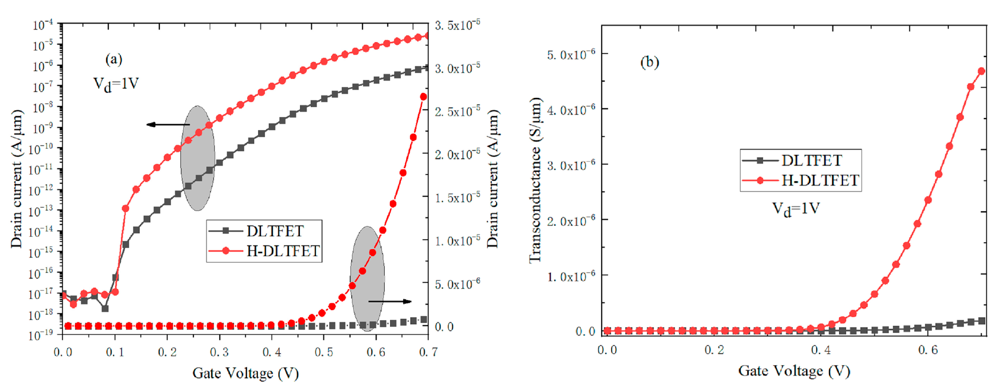
3.1. The Transfer and Output Characteristics Analysis

Figure 2a shows the transfer characteristics of DLTFET and H-DLTFET at Vg = 0.7 V, Vd = 1 V. The off-state currents of the two devices are basically the same, and the on-state currents of DLTFET and H-DLTFET are, respectively, 7.98 × 10⁻⁷ A/μm and 2.65 × 10⁻⁵ A/μm, so the on-state current and switching ratio are improved by almost two magnitude orders. The tunneling barrier width can be decreased by the introduction of Ge/SiGe heterojunction. The subthreshold swing (SS) is an important index for evaluating the performance of TFETs. When compared to the DLTFET, the point SS and average SS of H-DLTFET, respectively, decrease from 13 mV/Dec and 31.6 mV/Dec to 5 mV/Dec and 14.3 mV/Dec. Therefore, the H-DLTFET has better advantages in the low-voltage and low-power applications.
As an important parameter for evaluating the semiconductor devices simulation performance, the trans-conductance value is related to the transfer characteristics. The trans-conductance can be calculated by the first derivative of transfer characteristic [23], and the specific expression is shown in formula (1).
G m = d I d s / d V g s
In Figure 2b, the maximum trans-conductance of DLTFET and H-DLTFET are 1.79 × 10⁻⁷ S/μm and 4.68 × 10⁻⁶ S/μm, respectively. The trans-conductance value of DLTFET can be increased by an order of magnitude. The reason is that H-DLTFET has better transfer characteristics. Additionally, the larger the on-state current is, the better the trans-conductance performance is. The introduction of Ge/SiGe hetero-junction greatly optimizes the trans-conductance characteristics of H-DLTFET, so it better advantages in terms of frequency.
It can be clearly found by inspecting Figure 3a that the maximum output currents of DLTFET and H-DLTFET are 8.4 × 10⁻⁶A/μm and 1.1 × 10⁻⁴ A/μm, respectively. Additionally, the output current is increased by an order of magnitude, so the H-DLTFET has very obvious advantages in the output characteristics.
The output conductance can be obtained by the derivation of output conductance to drain voltage [24], which can be expressed by formula (2).
g d s = d I d s d V d s
In Figure 3b, the DLTFET and H-DLTFET devices achieve the maximum output conductance of 2.9 × 10⁻⁴ S/μm and 2.7 × 10⁻⁵ S/μm, respectively, at drain voltages of 0.38 V and 0.4 V, so the maximum output conductance value can be improved by an order of magnitude.

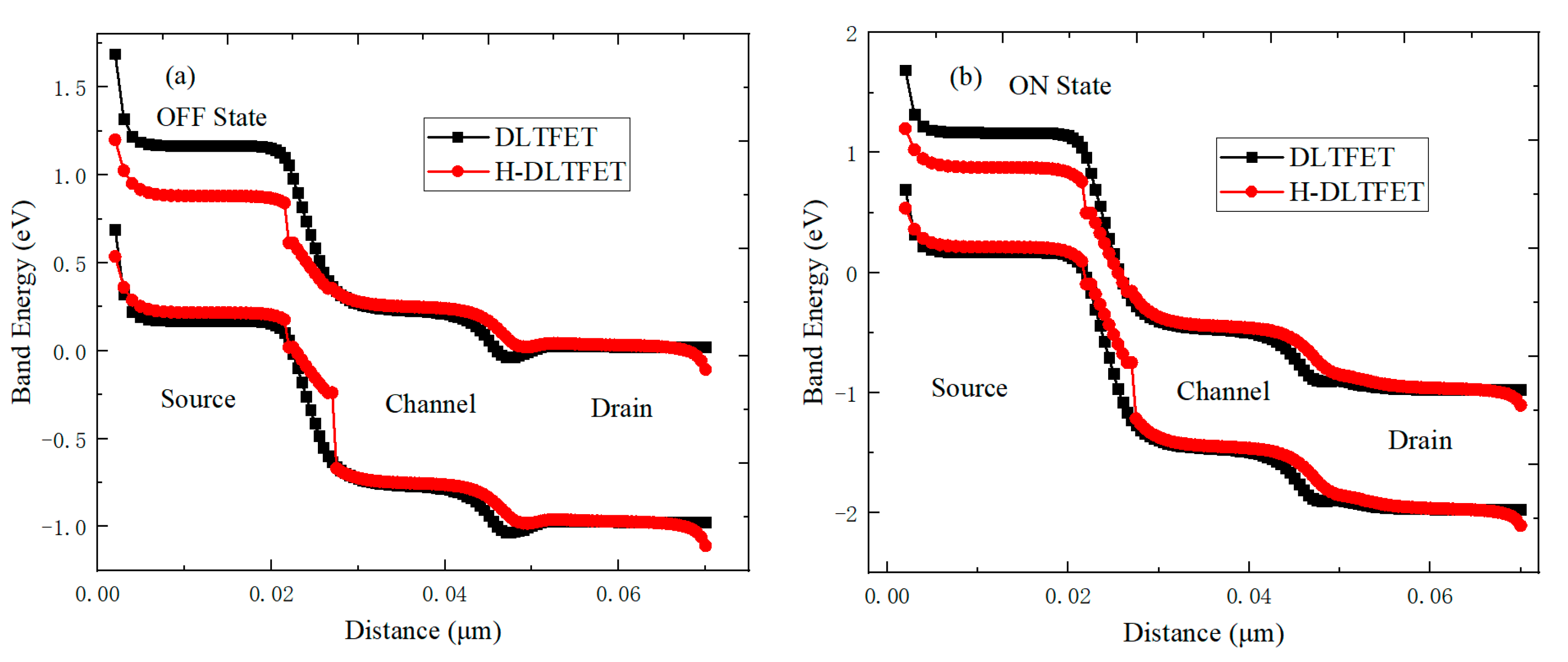
3.2. The Operating Mechanism of H-DLTFET

The electronic band tunneling rate distribution, total current density, electric field distribution, and potential distribution of H-DLTFET under the on-state (Vg = Vd = 1 V) are extracted to further analyze and master the working principle of H-DLTFET, as shown in Figure 4. It can be clearly seen from the electron band tunneling rate distribution that the tunneling area of H-DLTFET is mainly distributed on the surface between the source region and channel region, which conforms to the point tunneling rate distribution. The brightly colored area at the interface in Figure 4a is the point tunneling area. In Figure 4b, it can be seen from the total current density distribution that the tunneling electrons from the source region to the pocket region can pass through the channel region and be collected by drain region on the right to form the leakage current. Figure 4c shows the electric field distribution of the source/channel tunneling junction. The high electric field can effectively decrease the tunneling barrier width and the energy band becomes more curved, which can also promote the band tunneling phenomenon of electrons. It can be clearly seen by observing Figure 4d that there is the large potential gradient at the source/channel tunneling junction. Additonally, the energy band at the tunneling junction is bent, which is an indispensable condition for the band tunneling.
The corresponding energy bands of DLTFET and H-DLTFET are also extracted since the electron band tunneling mainly depends on the energy band barrier, as shown in Figure 5. In Figure 5a, the conduction band of channel region is not aligned with the valence band of source region under the off-state condition (Vd = 1 V, Vg = 0 V). At this time, there is no the same energy quantum state on both sides of tunneling junction, the electrons from source region can not pass through the barrier to channel region, so there is almost no tunneling current under the off state. By inspecting Figure 5b, it can be found that the energy band of channel region can be pulled down when the voltage is applied to the gate electrode. Meanwhile, the valence band of source region are aligned with the conduction band of channel region, there are the same energy quantum states on both sides of the tunneling junction. The tunneling current can be formed when the electrons from source region can pass through the barrier to channel region [25]. The barrier width at the tunneling junction decreases with the gate voltage increases, the same energy quantum states number on both sides of the tunneling junction increases, and the tunneling barrier width of DLTFET are smaller than that of H-DLTFET.

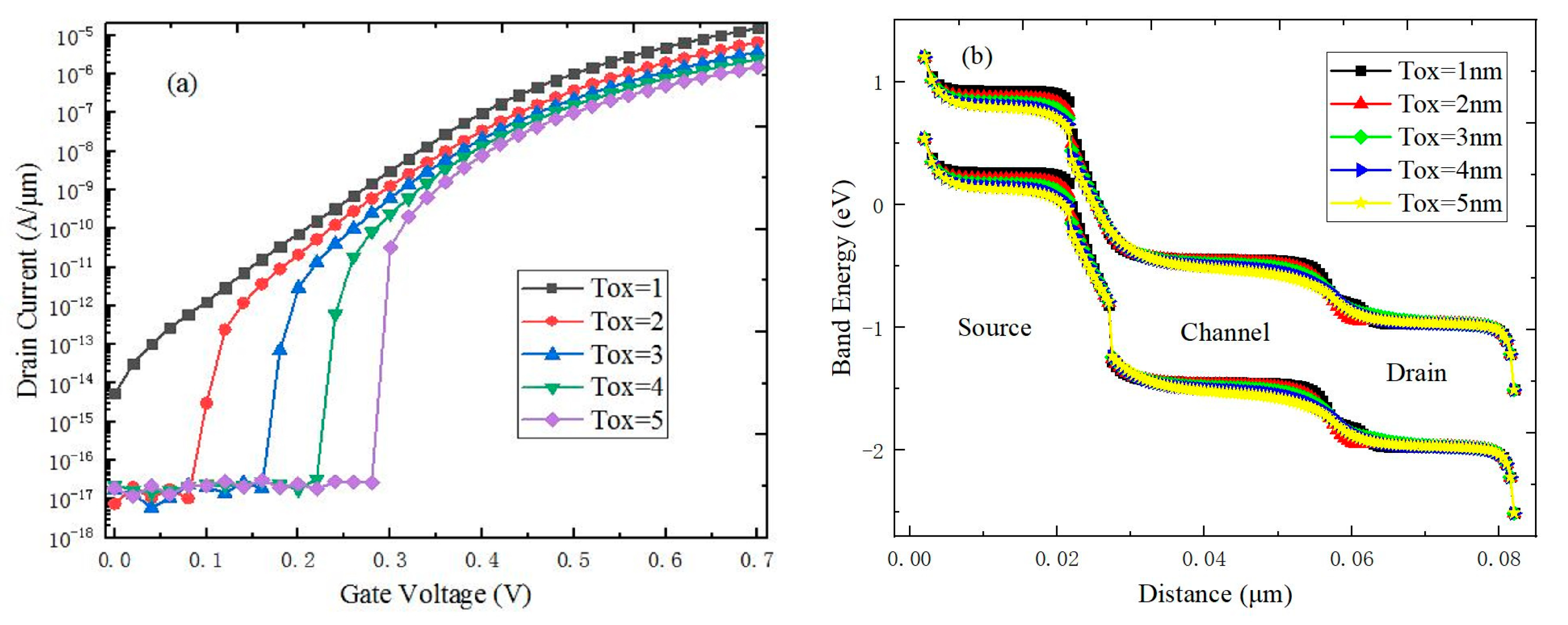
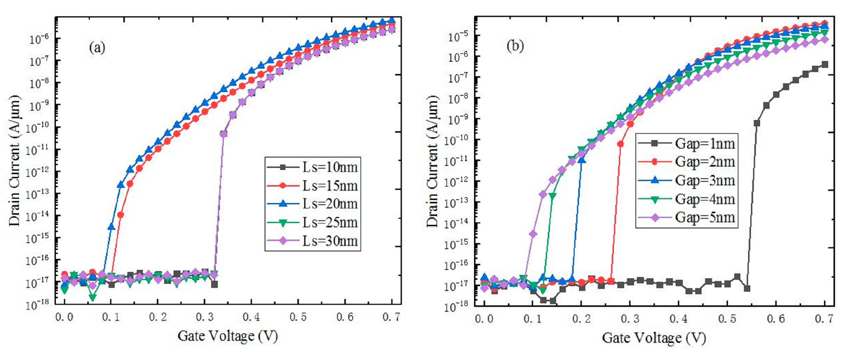
3.3. Effect of Device Parameters on The Electrical Performance

The band-tunneling phenomenon of H-DLTFET mainly depends on the doping concentration, device structure parameters, and electrode work function. It is necessary to optimize the device structure, doping concentration, and the electrode work function to obtain the better performance, such as the higher on-state current and lower gate-drain capacitance.
In Figure 6a, the doping concentration has little effect on the off-state current when doping concentration increase from 1 × 1018 cm−3 to 1 × 1019 cm−3, but on-state current is increased to a certain extent. The tunneling barrier width can be decreased when the doping concentration becomes higher. However, a slight fluctuation of doping concentration would cause the sharp increase of off-state current when the doping concentration is higher than 1 × 1019cm−3. The optimized doping concentration is 7 × 1018 cm−3 to avoid the influence of doping concentration fluctuation on the device performance. The tunneling barrier width between source region and channel regions decreases when the doping concentration increases from 1 × 1017 cm−3 to 2 × 1019 cm−3, as shown in Figure 6b. The energy band bending at the off-state tunneling junction mainly depends on the built-in electric field when the doping concentration is 2 × 1019 cm−3. The higher doping concentration increases the built-in electric field, thereby turning on the band tunneling under the off-state, which would increase the off-state current.
By observing Figure 7a, the turn-on voltage decreases with the source work function increases. Additionally, the continuous decrease of turn-on voltage would cause an increase of off-state current. The turn-on voltage of H-DLTFET is the negative gate voltage when the source work function is increased to 5.5 eV, and the off-state leakage current becomes larger. This is because the effective gate control capability increases when the source work function is increased, and the source/channel tunneling junction is turned on in advance, so the turn-on voltage decreases. Figure 7b shows the channel surface energy band under the on-state, the higher source work function can enhance the gate control capability and reduce the tunneling barrier width, and the channel energy bands are pulled down when the source work function increases, which means that the increase of source work function can allow for the tunneling junction to reach the band tunneling efficiency conditions at a lower gate voltage.
Figure 8a shows the transfer characteristics of H-DLTFET under the different gate work functions; gate work function has the relatively large effect on off-state current, on-state current, and turn-on voltage. As the gate work function decreases, the turn-on voltage decreases. The continuous decrease of turn-on voltage would lead to the increase of off-state current and on-state current. It can be seen from Figure 8b that the smaller gate work function can enhance the gate control ability, the channel energy band is pulled down, and the tunneling barrier width decreases, so the electron generation band tunneling efficiency of the channel is significantly improved.
Figure 9a shows the leakage drain current of H-DLTFET under the different gate oxide layer thicknesses. It can be seen that there is almost no change of the off-state leakage drain current when the gate oxide layer thickness exceeds 2 nm, and the on-state current decreases with the gate oxide thickness increases. The off-state leakage current of H-DLTFET significantly increases when the gate oxide layer thickness is 1nm. The electrons from source region tunneled flow to the drain region along the channel and oxide interface, so the energy band along the channel interface is extracted, as shown in Figure 9b. The barrier width of the tunneling junction decreases when the gate oxide thickness becomes thinner, and the energy band becomes more steeply curved. The electrons from source region more easily penetrate into the channel region, and the energy band tunneling phenomenon easily occurs.
Figure 10a shows the leakage drain current of H-DLTFET under the different channel thicknesses. The on-state current increases as the channel thickness decreases. In order to avoid the fluctuation influence of channel height on the device performance in the actual process, the optimal channel thickness is selected to be 5 nm. In Figure 10b, the thinner channel thickness can help to promote the energy band bending, which would decrease the tunneling barrier width. Besides, the electrons from source region can tunnel to drain region along the channel and oxide interface.
The on-state current increases when Ls increase from 10 nm to 20 nm, the threshold voltage decreases, and the off-state current does not change significantly, as shown in Figure 11a. However, the on-state current decreases when Ls increase from 20 nm to 30 nm, and the threshold voltage increases, so the optimal source region length is 20 nm. In Figure 11b, the threshold voltage of device decreases as the pocket length increases, and the device is more easily turned on at the lower voltage. Therefore, the optimal pocket length of SiGe material is 5 nm in order to avoid the fluctuation influence of gap length on device performance in the actual process.

3.4. The C-V Characteristics

The capacitance characteristics are helpful in calculating the frequency characteristics and switching characteristics of the integrated circuits. The miller capacitance mainly affects the frequency characteristics of analog circuits and the delay characteristics of digital circuits [26]. The delay of digital circuit is directly proportional to the miller capacitance, and the frequency of analog circuit is inversely proportional to the miller capacitance, so it is necessary to decrease the miller capacitance value [27]. When the gate voltage increase, the inversion layer of TFET expands from the channel surface to source region, and the inversion layer can be formed on the entire channel region surface. The miller capacitance of TFETs with energy band tunneling is mainly composed of gate-drain capacitance, while the gate-source capacitance has a little effect on miller capacitance. Using the heterogeneous gate dielectric mainly reduces the gate-drain capacitance. The gate oxide layer near source region uses the high-k HfO2 material to maintain the high gate control ability, and the gate oxide layer near the drain region uses the low-k SiO2 material to decrease the gate-drain overlap capacitance. It is concluded that the heterogeneous gate dielectric can significantly decrease the gate-drain capacitance.
It can be seen from Figure 12 that the gate-source capacitance of two devices remains basically unchanged when the gate voltage increases, and the gate capacitance increases with the gate-drain capacitance increases, which indicates that the gate capacitance is mainly dependent on the gate-drain capacitance. The gate capacitance of DLTFET is higher than that of H-DLTFET. This is because the gate dielectric near drain region under the auxiliary gate uses the low-k SiO2 dielectric material. When compared to the DLTFET, the gate-drain capacitance of H-DLTFET decrease from 0.99 fF/μm to 0.1 fF/μm under the on-state condition (Vg = 0.7 V, Vd = 1 V), which indicates that this method is effective in decreasing the capacitive.

3.5. The Frequency Characteristics

The frequency characteristics take the trans-conductance and the capacitance characteristics into account, which can better reflect the application potential of device in the analog integrated circuits [28]. The cut-off frequency reflects the highest amplification frequency of device, which is one of the key parameters of analog circuits. The cut-off frequency is related to the gate capacitance and trans-conductance [29,30], which can be expressed by the equation (3). As shown in equation (3), fT, gm, Cgs, Cgd, and Cgg, respectively, represent the cut-off frequency, trans-conductance, gate-source capacitance, gate-drain capacitance, and gate-gate capacitance.
f t = g m 2 π C g s 1 + 2 C g d / C g s g m 2 π ( C g s + C g d ) = g m 2 π C g g
It can be observed from the frequency characteristics that the cut-off frequencies of DLTFET and H-DLTFET are, respectively, 0.03 GHz and 3.25 GHz. The H-DLTFET has the better advantages in the analog integrated circuits, because it has the better trans-conductance, DC characteristics, and smaller capacitance values.
The gain bandwidth product with the DC gain of 10 can be calculated by the ratio of trans-conductance and gate-drain capacitance [31,32]. Formula (4) shows the specific calculation formula, wherein the gain bandwidth product, trans-conductance, and gate-drain capacitance can be represented by GWB, gm, Cgd.
G W B = g m 2 π 10 C g d
In Figure 13b, the gain bandwidth products of two devices can respectively reach 0.003GHz and 0.703GHz. The H-DLTFET has the better gain bandwidth product; the change trend of gain bandwidth product with gate voltage is the same as the cut-off frequency, which is caused by the change of trans-conductance and gate-drain capacitance with the gate voltage. The cut-off frequency and gain bandwidth product of H-DLTFET are much larger than that of DLTFET. This is because the H-DLTFET has the excellent DC characteristics. Besides, the H-DLTFET has better frequency characteristics, so it is more suitable for the analog integrated circuits.

4. Conclusions

This paper compares the analog circuit and frequency performance of DLTFET and H-DLTFET with Silvaco TCAD software in detail. First, the structural parameters, models, and band structures of two devices are briefly introduced. Subsequently, the input and output characteristics are compared and analyzed. Next, the working principle of H-DLTFET can be described. Subsequently, the effects of device parameters, doping concentration, and electrode work function on the device electrical performance are systematically analyzed from the band angle. Subsequently, the capacitance and frequency characteristics of two devices are compared. When compared to the traditional DLTFET, the on-state current, switching ratio, trans-conductance, output current, and output conductance value of the newly constructed H-DLTFET are, respectively, improved by two, two, one, one, and one order of magnitude. The point SS and average SS of H-DLTFET, respectively, decrease from 13 mV/Dec and 31.6 mV/Dec to 5 mV/Dec and 14.3 mV/Dec, and the gate-drain capacitance decreases from 0.99 fF/μm to 0.1 fF/μm. Moreover, the cut-off frequency and gain bandwidth product of H-DLTFET are much larger than that of DLTFET, which is due to the excellent DC characteristics. The H-DLTFET has better frequency characteristics, which is suitable for applications of the ultra-low power integrated circuits.

Author Contributions

Conceptualization and writing—original draft preparation, T.H.; methodology, S.W.; validation, S.C. and H.X.; writing—review and editing, H.L.; funding acquisition, H.L. All authors have read and agreed to the published version of the manuscript.

Funding

This research was funded by the National Natural Science Foundation of China (Grant Nos. U1866212 and 61904136), the Foundation for Fundamental Research of China (Grant No. JSZL2016110B003), the Major Fundamental Research Program of Shaanxi (Grant No. 2017ZDJC-26), the Innovation Foundation of Radiation Application (Grant No.KFZC2018040206). It was also supported by the Fundamental Research Funds for the Central Universities, and the Innovation Fund of Xidian University.

Conflicts of Interest

The authors declare no conflicts of interest.

References

  1. Kim, S.W.; Kim, J.H.; Liu, T.J.K.; Choi, W.Y.; Park, B.G. Demonstration of L-shaped tunnel field-effect transistors. IEEE Trans. Electron Devices 2016, 63, 1774–1778. [Google Scholar] [CrossRef]
  2. Wang, W.; Wang, P.; Zhang, C.; Lin, X.; Liu, X.; Sun, Q.; Zhou, P.; Zhang, D.W. Design of U-Shape Channel Tunnel FETs with SiGe Source Regions. IEEE Trans. Electron Devices 2014, 61, 193–197. [Google Scholar] [CrossRef]
  3. Rahi, S.B.; Asthana, P.; Gupta, S. Heterogate junctionless tunnel field-effect transistor: Future of low-power devices. J. Comput. Electron. 2016, 16, 33–38. [Google Scholar] [CrossRef]
  4. Lee, H.; Park, S.; Lee, Y.; Nam, H.; Shin, C. Random variation analysis and variation-aware design of symmetric tunnel field-effect transistor. IEEE Trans. Electron Devices 2015, 62, 1778–1783. [Google Scholar]
  5. Li, W.; Liu, H.; Wang, S.; Chen, S. Reduced Miller capacitance in U-shaped channel tunneling FET by introducing heterogeneous gate dielectric. IEEE Trans. Electron Devices 2017, 38, 403–406. [Google Scholar] [CrossRef]
  6. Raushan, M.A.; Alam, N.; Akram, M.W.; Siddiqui, M.J. Impact of asymmetric dual-k spacers on tunnel field effect transistors. J. Comput. Electron. 2018, 17, 756–765. [Google Scholar] [CrossRef]
  7. Cao, J.; Logoteta, D.; Özkaya, S.; Biel, B.; Cresti, A.; Pala, M.G.; Esseni, D. Operation and Design of van der Waals Tunnel Transistors: A 3-D Quantum Transport Study. IEEE Trans. Electron Devices 2016, 63, 4388–4394. [Google Scholar] [CrossRef]
  8. Wadhwa, G.; Raj, B. Label Free Detection of Biomolecules Using Charge-Plasma-Based Gate Underlap Dielectric Modulated Junctionless TFET. J. Electron. Mater. 2018, 47, 4683–4693. [Google Scholar] [CrossRef]
  9. Rahi, S.B.; Ghosh, B.; Bishnoi, B. Temperature effect on hetero structure junctionless tunnel FET. J. Semicond. 2015, 36, 034002. [Google Scholar] [CrossRef]
  10. Singh, G.; Amin, S.I.; Anand, S.; Sarin, R.K. Design of Si0.5Ge0.5 based tunnel field effect transistor and its performance evaluation. Superlattices Microstruct. 2016, 92, 143–156. [Google Scholar] [CrossRef]
  11. Dash, S.; Mishra, G.P. A new analytical threshold voltage model of cylindrical gate tunnel FET (CG-TFET). Superlattices Microstruct. 2015, 86, 211–220. [Google Scholar] [CrossRef]
  12. Chauhan, S.S.; Sharma, N. Impact of Spacer-Gate Engineered Workfunction on the Performance of Dopingless TFET. J. Nanoelectron. Optoelectron. 2018, 13, 1200–1203. [Google Scholar] [CrossRef]
  13. Damrongplasit, N.; Kim, S.H.; Liu, T.J.K. Study of random dopant fluctuation induced variability in the raised-Ge-source TFET. IEEE Electron Device Lett. 2013, 34, 184–186. [Google Scholar] [CrossRef]
  14. Raad, B.R.; Nigam, K.; Sharma, D.; Kondekar, P.N. Performance investigation of bandgap, gate material work function and gate dielectric engineered TFET with device reliability improvement. Superlattices Microstruct. 2016, 94, 138–146. [Google Scholar] [CrossRef]
  15. Anand, S.; Sarin, R.K. Gate misalignment effects on analog/RF performance of charge plasma-based doping-less tunnel FET. Appl. Phys. A 2017, 123, 413. [Google Scholar] [CrossRef]
  16. Cecil, K.; Singh, J. Influence of Germanium source on dopingless tunnel-FET for improved analog/RF performance. Superlattices Microstruct. 2017, 101, 244–252. [Google Scholar] [CrossRef]
  17. Revelant, A.; Villalon, A.; Wu, Y.; Zaslavsky, A.; Le Royer, C.; Iwai, H.; Cristoloveanu, S. Electron-hole bilayer TFET: Experiments and comments. IEEE Trans. Electron Devices 2014, 61, 2674–2681. [Google Scholar]
  18. Aslam, M.; Sharma, D.; Yadav, S.; Soni, D.; Sharma, N.; Gedam, A. A comparative investigation of low work-function metal implantation in the oxide region for improving electrostatic characteristics of charge plasma TFET. Micro. Nano. Lett. 2019, 14, 123–128. [Google Scholar] [CrossRef]
  19. Lahgere, A.; Panchore, M.; Singh, J. Dopingless ferroelectric tunnel FET architecture for the improvement of performance of dopingless n-channel tunnel FETs. Superlattices Microstruct. 2016, 96, 16–25. [Google Scholar]
  20. Anand, S.; Sarin, R.K. An analysis on ambipolar reduction techniques for charge plasma based tunnel field effect transistors. J. Nanoelectron. Optoelectron. 2016, 11, 543–550. [Google Scholar] [CrossRef]
  21. Tirkey, S.; Nigam, K.; Pandey, S.; Sharma, D.; Kondekar, P. Investigation of gate material engineering in junctionless TFET to overcome the trade-off between ambipolarity and RF/linearity metrics. Superlattices Microstruct. 2017, 109, 307–315. [Google Scholar]
  22. Han, T.; Liu, H.; Chen, S.; Wang, S.; Li, W. A Doping-Less Tunnel Field-Effect Transistor with Si0.6Ge0.4 Heterojunction for the Improvement of the On–Off Current Ratio and Analog/RF Performance. Electronics 2019, 8, 574. [Google Scholar] [CrossRef] [Green Version]
  23. Bagga, N.; Sarkar, S.K. An analytical model for tunnel barrier modulation in triple metal double gate TFET. IEEE Trans. Electron Devices 2015, 62, 2136–2142. [Google Scholar] [CrossRef]
  24. Singh, D.; Pandey, S.; Nigam, K.; Sharma, D.; Yadav, D.S.; Kondekar, P. A charge-plasma-based dielectric-modulated junctionless TFET for biosensor label-free detection. IEEE Trans. Electron Devices 2017, 64, 271–278. [Google Scholar] [CrossRef]
  25. Leung, G.; Chui, C.O. Variability Impact of Random Dopant Fluctuation on Nanoscale Junctionless FinFETs. IEEE Electron Device Lett. 2012, 33, 767–769. [Google Scholar] [CrossRef]
  26. Lattanzio, L.; De Michielis, L.; lonescu, A.M. The electron–hole bilayer tunnel FET. Solid-State Electron. 2012, 74, 85–90. [Google Scholar] [CrossRef]
  27. Padilla, J.L.; Alper, C.; Medina-Bailón, C.; Gámiz, F.; lonescu, A.M. Assessment of pseudo-bilayer structures in the heterogate germanium electron-hole bilayer tunnel field-effect transistor. Appl. Phys. Lett. 2015, 106, 262102. [Google Scholar] [CrossRef] [Green Version]
  28. Ghosh, B.; Akram, M.W. Junctionless tunnel field effect transistor. IEEE Electron Device Lett. 2013, 34, 584–586. [Google Scholar] [CrossRef]
  29. Kao, K.H.; Verhulst, A.S.; Vandenberghe, W.G.; Sorée, B.; Magnus, W.; Leonelli, D.; Groeseneken, G.; De Meyer, K. Optimization of gate-on-source-only tunnel fets with counter-doped pockets. IEEE Trans. Electron Devices 2012, 59, 2070–2077. [Google Scholar] [CrossRef]
  30. Asthana, P.K.; Goswami, Y.; Basak, S.; Rahi, S.B.; Ghosh, B. Improved performance of a junctionless tunnel field effect transistor with a Si and SiGe heterostructure for ultra low power applications. RSC Adv. 2015, 5, 48779–48785. [Google Scholar] [CrossRef]
  31. Biswas, A.; Luong, G.V.; Chowdhury, M.F.; Alper, C.; Zhao, Q.; Udrea, F. Benchmarking of Homojunction Strained-Si NW Tunnel FETs for Basic Analog Functions. IEEE Trans. Electron Devices 2017, 64, 1441–1448. [Google Scholar] [CrossRef]
  32. Sze, S.M.; Kwok, K.N.G. Physics of Semiconductor Devices, 3rd ed.; XI’AN JIAOTONG UNIVERSITY PRESS: Xi’an, China, 2008; pp. 130–246. [Google Scholar]
Figure 1. The device structure of (a) traditional doping-less tunneling field effect transistor (DLTFET), (b) new constructed hetero-gate dielectric (H-DLTFET).
Coatings 10 00278 g001
Figure 2. (a) The transfer characteristics comparison, (b) The trans-conductance values comparison of DLTFET and H-DLTFET.
Coatings 10 00278 g002
Figure 3. (a) The output characteristics, (b) The output conductance of DLTFET and H-DLTFET.
Coatings 10 00278 g003
Figure 4. The working principle introduction of H-DLTFET (a) e-BTBT tunneling efficiency; (b) total current density; (c) electric field distribution; and, (d) potential.
Coatings 10 00278 g004
Figure 5. The energy band change schematic diagram from source region to drain region of DLTFET and H-DLTFET. (a) Off-state energy band distribution; (b) on-state energy band distribution.
Coatings 10 00278 g005
Figure 6. (a) The transfer characteristics variation with doping concentration; (b) The on-state energy band diagrams under the different doping concentration.
Coatings 10 00278 g006
Figure 7. (a) Effect of source work function on the transfer characteristics; (b) The on-state energy band distribution of H-DLTFET under the different source work functions.
Coatings 10 00278 g007
Figure 8. (a) Effect of gate work function on transfer characteristics; (b) The on-state energy band distribution of H-DLTFET under the different gate work functions.
Coatings 10 00278 g008
Figure 9. (a) Effect of gate oxide thickness on the transfer characteristics of H-DLTFET; (b) The on-state energy band under the different gate oxide thickness.
Coatings 10 00278 g009
Figure 10. (a) Effect of channel height on the transfer characteristics of H-DLTFET, (b) The on-state energy band under the different channel thickness.
Coatings 10 00278 g010
Figure 11. (a) Effect of channel height on transfer characteristics, (b) Effect of pocket length on transfer characteristics.
Coatings 10 00278 g011
Figure 12. Capacitance characteristic analysis of (a) DLTFET; (b) H-DLTFET.
Coatings 10 00278 g012
Figure 13. (a) Cut-off frequency; (b) Gain bandwidth product.
Coatings 10 00278 g013

