Article

Effects of the Nitrogen Flow Ratio and Substrate Bias on the Mechanical Properties of W–N and W–Si–N Films

1
Department of Materials Engineering, Ming Chi University of Technology, New Taipei City 24301, Taiwan
2
Center for Plasma and Thin Film Technologies, Ming Chi University of Technology, New Taipei City 24301, Taiwan
3
Department of Optoelectronics and Materials Technology, National Taiwan Ocean University, Keelung 20224, Taiwan
4
Undergraduate Program in Optoelectronics and Materials Technology, National Taiwan Ocean University, Keelung 20224, Taiwan
5
Center of Excellence for Ocean Engineering, National Taiwan Ocean University, Keelung 20224, Taiwan
*
Author to whom correspondence should be addressed.
Coatings 2020, 10(12), 1252; https://doi.org/10.3390/coatings10121252
Submission received: 25 November 2020 / Revised: 14 December 2020 / Accepted: 16 December 2020 / Published: 18 December 2020
(This article belongs to the Special Issue New Hard and Superhard Coatings)

Abstract

:
The reactive gas flow ratio and substrate bias voltage are crucial sputtering parameters for fabricating transition metal nitride films. In this study, W–N films were prepared using sputtering with nitrogen flow ratios (f) of 0.1–0.5. W–N and W–Si–N films were then prepared using an f level of 0.4 and substrate bias varying from 0 to −150 V by using sputtering and co-sputtering, respectively. The variations in phase structures, bonding characteristics, mechanical properties, and wear resistance of the W–N and W–Si–N films were investigated. The W–N films prepared with nitrogen flow ratios of 0.1–0.2, 0.3, and 0.4–0.5 displayed crystalline W, amorphous W–N, and crystalline W2N, respectively. The W–N films prepared using a nitrogen flow ratio of 0.4 and substrate bias voltages of −50 and −100 V exhibited favorable mechanical properties and high wear resistance. The mechanical properties of the amorphous W–Si–N films were not related to the magnitude of the substrate bias.

1. Introduction

W–N films were developed as hard coatings and display remarkable mechanical properties [1,2,3,4,5,6,7]. The phase of W–N films varies from α-W to β-W, β-W2N, and δ-WN as the N concentration increases [8,9]. The β-W2N phase is a B1 structure, in which N atoms occupy half of the octahedral interstitial sites of cubic close-packed W atoms [9,10,11]. The cubic W2N phase formed in W–N films has been extensively discussed in the literature, whereas the hexagonal WN phase, fabricated using sputtering processes, has been only recently observed by applying high reactive gas flow ratios, accompanied with a high N concentration in the films [2,9]. Polcar et al. [3] reported that δ-WN forms in sputtered W–N films containing >55 at.%. Baker and Shah [10] reported that a saturated N concentration of 35 at.% in W–N films for a W2N phase could be obtained by sputtering. Similar phase variations from W2N to WN were reported for W–N films prepared using the cathodic arc method, with N2 flow ratios exceeding 0.35 [12]. However, Lou et al. [7] did not report hexagonal or cubic WN phases, even in W–N films fabricated by the superimposed high-power impulse magnetron sputtering and mid-frequency pulses system by using a high N2 flow ratio of up to 74%, which formed an N/W ratio of 0.60. The hardness (H) levels of α-W, β-W2N, and δ-WN were 13, 24, and 28 GPa, respectively [12]. Therefore, W–N films with β-W2N and δ-WN phases ensured a high level of hardness. A study [13] reported that sputtered W78N22 films exhibited an H of 33.3 GPa and Young’s modulus (E) of 338 GPa; the H value was comparable with the reported at 31.6–34.5 GPa for films with a W2N phase [2,5,7,14]. One of the main aims of this study was to explore the effects of the nitrogen flow ratio and substrate bias on the structural development and mechanical properties of W–N films. The application of negative substrate bias during sputtering is favored to form compressive residual stress or a preferred orientation on deposited films, which tend to increase the film hardness [15,16]. Studies [9,17] have reported that substrate bias affects the characteristics of W–N films. Substrate bias induces the re-sputtering of N atoms. However, the crystal structure, bonding state, and composition variations related to the magnitude of the applied bias were insignificant [9]. The characteristics of W–N films, such as mechanical properties, thermal stability, and oxidation resistance, could be further enhanced by adding Si, which forms nanocomposite or near-amorphous structures [18,19,20,21,22,23,24]. The mechanical properties of M–Si–N thin films are affected by strengthening mechanisms involving the formation of a solid-solution and nanocomposite structure and the residual stress effect [25]. In our previous study [13], the H of co-sputtered W–Si–N films reduced from 33.3 to 14.7 GPa as the Si concentration increased from 0 to 24 at.%, accompanied by a phase change from a crystalline to an amorphous and crystalline mix and finally to an amorphous structure. Bias sputtering increased the kinetic energy of charged ions, which enhanced the mobility of sputtered species and resulted in re-sputtering and atomic peening [26,27,28]. The re-sputtering of light adatoms could affect the atomic compositions of M–Si–N films [29,30]. Therefore, this study investigated variations in the mechanical properties and wear resistance of sputtered W–N and W–Si–N films by adjusting the nitrogen flow ratio and substrate bias.

2. Materials and Methods

The sputtering processes for fabricating the W–N and W–Si–N films and Ti interlayers have been previously illustrated [13]. Si wafers and stainless steel (SUS 420) were the substrates used in this study. The aforementioned films, fabricated on stainless steel substrates, were utilized for the pin-on-disk test. The substrates were fixed on a substrate holder, which was rotated at 5 rpm and electrically grounded during depositing of the Ti interlayers. Four batches of samples, namely W, A, B, and C, were prepared. Batch W samples were prepared using a W target power (PW) of 150 W and various nitrogen flow ratios [f = N2/(N2 + Ar)] of 0.1, 0.2, 0.3, 0.4, and 0.5. Batch A samples were fabricated using Pw of 150 W, f of 0.4, and negative bias voltages of 0, 25, 50, 100, and 150 V. Batch B samples were co-sputtered using PW of 150 W and Si target power (PSi) of 150 W and an f of 0.4 under compressive bias levels of 0, 25, 50, and 100 V, whereas Batch C samples were fabricated using PW of 60 W and PSi of 150 W and an f of 0.4 under compressive bias levels of 0, 25, 50, and 100 V.
The atomic compositions of the films were analyzed by a field-emission electron probe microanalyzer (FE-EPMA, JXA-8500F, JEOL, Akishima, Japan). The phases and lattice constants of the films were analyzed using the grazing incident X-ray diffraction technique (GIXRD, X’Pert PRO MPD, PANalytical, Almelo, The Netherlands), with an incidence angle of 1°. The lattice constant, α0, of each crystalline film was determined with the following equation [31]:
α = α 0 + K × cos 2 θ sin θ
where α is the lattice constant for the individual reflection, K is constant, and θ is the diffraction angle. The X-ray diffraction (XRD) patterns for determining the texture coefficients and grain sizes of films followed a Bragg–Brentano (θ–2θ) scan. The texture coefficient, Tc, was defined as [32]:
T c ( h k l ) = I m ( h k l ) I 0 ( h k l ) [ 1 n n = 1 n I m ( h k l ) I 0 ( h k l ) ] 1
where Im(hkl) is the measured relative reflection intensity of the (hkl) plane, I0(hkl) is the relative intensity from the standard reference, and n, the number of reflections, is two in this study. The grain sizes were calculated using the Scherrer formula [31]. The H and E of the films were measured using a nanoindentation tester (TI-900 Triboindenter, Hysitron, Minneapolis, MN, USA) equipped with a Berkovich diamond probe tip. The indentation depth was 50 nm following the 1/10 rule used for determining the mechanical properties of thin films [33]. The H and reduced elastic modulus values were calculated based on the Oliver and Pharr method [34]. The average surface roughness (Ra) values of the films were evaluated by using an atomic force microscope (Dimension 3100 SPM, Nanoscope IIIa, Veeco, Santa Barbara, CA, USA) with a scanned area of 5 × 5 μm2. The residual stress of the films on Si substrates was determined using Stoney’s equation [35], which was previously illustrated [36]. The thickness of the Si substrate is 525 μm. The bonding characteristics of the elements were examined by using an X-ray photoelectron spectroscope (XPS, PHI 1600, PHI, Kanagawa, Japan) with an Mg Kα X-ray. The wear resistance of films was examined through the pin-on-disk test. A cemented tungsten carbide (WC–6 wt.% Co) ball, 6 mm in diameter, was used as the stationary pin. The normal load was 2 N, the sliding speed was 104.5 mm/s, the wear track diameter was 16 mm, and the wear length was 200 m.

3. Results and Discussion

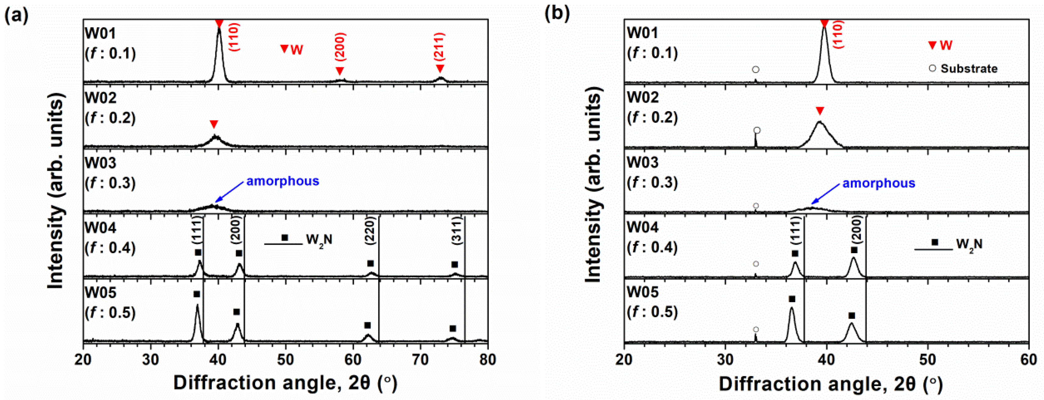
3.1. W–N Films Prepared with Various Nitrogen Flow Ratios

The atomic compositions of the Batch W films fabricated with f levels of 0.1–0.5 are displayed in Table 1. These samples were labeled W01, W02, W03, W04, and W05 for the f level sets of 0.1, 0.2, 0.3, 0.4, and 0.5, respectively. These samples had Si concentrations of 0.5–1.9 at.%, which originated from Si substrates because these films had smaller thicknesses (511–675 nm). The N concentration increased from 4.7 to 8.3, 12.4, 22.5, and 25.3 at.% as the f level increased from 0.1 to 0.2, 0.3, 0.4, and 0.5, respectively, whereas the W concentration decreased from 93.6 to 85.9, 80.5, 75.4, and 72.8 at.%, respectively. Studies [1,7,37] have reported that an increase in the f level causes an elevation in the N/W ratio of W–N films. The N/W ratios were 0.05, 0.10, 0.15, 0.30, and 0.35 for the W01, W02, W03, W04, and W05 films, respectively. This variation was accompanied by the film phase changing from α-W to amorphous and β-W2N, as illustrated in Figure 1a. Similar phase variations with increasing f were reported without applying substrate bias [17]. Moreover, the increase in compressive residual stress from 0 to 2.4 GPa was related to an increase in the N/W ratio. The GIXRD pattern of W01 films displayed a body-centered cubic phase with (110), (200), and (211) reflections, whereas the GIXRD pattern of the W02 films only exhibited a W(110) reflection, with an intensity decrease relative to that of the W01 films. The GIXRD patterns of the W04 and W05 films exhibited a face-centered cubic (FCC) phase with (111), (200), (220), and (311) reflections. Figure 1b presents the Bragg–Brentano scan XRD patterns of the Batch W samples. The grain sizes of the W01 and W02 films were determined to be 10.2 and 4.4 nm, respectively, by using the full width at half maximum (FWHM) of (110) reflections. The reduction in the deposition rate from 8.4 to 7.7 and 7.1 nm/min with an increase in the f level from 0.1 to 0.2 and 0.3 could be attributed to the reduction in sputtering yield. The standard intensity ratio of (111):(200) for the W2N phase was 100:47, whereas the W04 and W05 films exhibited the (200) texture, as determined using Equation (2) and reflection intensities from Figure 1b. The texture coefficients (Tcs) were 0.46 and 1.54 for Tc(111) and Tc(200) of the W04 films, respectively, whereas the texture values were 0.76 and 1.24 for Tc(111) and Tc(200) of W05 films, respectively. The deposition rates were 7.3 and 6.4 nm/min for the W04 and W05 films, respectively. These values were affected by the target poisoning effect.
Figure 2 presents the XPS profiles of the N 1s and W 4f core levels of Batch W samples at a depth of 54 nm. The intensity ratio of N signals was 1.0:2.1:3.1:4.7:6.0 for W01:W02:W03:W04:W05. The W profile was deconvoluted into two 4f doublets, representing W–W and W–N bonding, accompanied by a minor W 5p3/2 component. Table 2 summarizes the XPS analysis results of the W–N films at depths of 27, 36, 45, and 54 nm. The intensity ratios of W–W:W–N for the Batch W samples varied from 84:16, to 75:25, 74:26, 72:28, and 70:30 as the f level increased from 0.1, to 0.2, 0.3, 0.4, and 0.5, respectively. The increase in the f level increased the N concentration and the amount of W–N bonds in the Batch W films. Table 3 lists the mechanical properties of the W–N films. The W01 films with zero residual stress exhibited an H of 22.4 GPa and an E of 335 GPa. The H and E of the W02 films increased to 26.2 and 388 GPa, respectively, which can be attributed to the lower grain size and residual stress of −0.7 GPa. The W03 films exhibited a lower H and E of 22.1 and 308 GPa, respectively, caused by the formation of an amorphous phase. The W04 and W05 films with a W2N phase exhibited H levels of 25.9 and 29.6 GPa and residual stresses of −1.6 and −2.4 GPa, respectively, as well as E values of approximately 350 GPa. H/E [38] and H/E* (E*: effective Young’s modulus) [39] represent the elastic strain to failure. Films with H/E* > 0.1 and We ≥ 60% displayed high toughness [39]. H3/E2 [40] and H3/E*2 [41] reflect the resistance to plastic deformation, and are used to evaluate wear resistance [42]. The H/E and H3/E2 ratios and elastic recovery (We) of the Batch W samples increased with increasing f levels. The wear tests of the W01 and W04 films were examined in Section 3.4. Studies [43,44,45] have reported that the films with high surface roughness values exhibit larger deviations and lower averages of mechanical properties evaluated using a nanoindentation technique. Except for the W02 sample with a high Ra of 13.23 nm, all the films in this study exhibited a low Ra level (<5 nm). The effects of Ra on the mechanical properties were insignificant. A nitrogen flow ratio f of 0.4 was sufficient to fabricate films with a W2N phase which exhibited satisfactory mechanical properties. Therefore, an f of 0.4 was utilized in the next section to evaluate the substrate bias effects on the characteristics of W–N films.

3.2. W–N Films Prepared with Various Bias Voltages

Table 1 displays the atomic compositions and thicknesses of the W–N films (Batch A) prepared using a power of 150 W, an f level of 0.4, and substrate bias voltages varying from 0 to −150 V. The samples A0 and W04 were the same. The Batch A samples were prepared using only a W target and displayed a low Si concentration of 0.7–3.9 at.%, which was attributed to low thickness values (521–610 nm). Furthermore, the Si concentrations originated from the Si substrates. Except for the A25 samples, the thicknesses and deposition rates of the films prepared through bias sputtering were lower compared with those of the films prepared at grounded state (A0), indicating the occurrence of re-sputtering. Figure 3a depicts the GIXRD patterns of the Batch A films, which exhibit an FCC W2N phase. Most W–N films fabricated using sputtering processes were reported to crystallize into a β-W2N phase. Polcar et al. [3,8] have reported mixed δ-WN and β-W2N phases in W42N58 coatings, with an N/W ratio of 1.38. In the present study, the N/W ratios of Batch A films were 0.30–0.44 (Table 1), with a β-W2N phase. Moreover, an expanded lattice formed because all W2N reflections shifted toward lower 2θ angle levels. Figure 4 displays the lattice parameters of these crystalline W–N coatings, determined using Equation (1). The lattice constants of the A0, A25, A50, A100, and A150 samples were 0.4199, 0.4198, 0.4202, 0.4201, and 0.4208 nm, respectively. The standard lattice constant of the β-W2N phase was 0.4126 nm [ICDD 00-025-1257] (ICDD: International Centre for Diffraction Data). The lattice constants of the Batch A films exhibited expanded lattices accompanied with compressive residual stresses. Figure 3b illustrates the Bragg–Brentano scan XRD patterns of the Batch A films. Figure 5 displays the Tcs of the Batch A samples, determined using Equation (2), and the Tcs of the W05 samples are also illustrated. All the crystalline W–N films displayed a (200) orientation accompanied by high compressive stresses ranging from −1.6 to −3.2 GPa.
The XPS analysis results of the Batch A films are displayed in Table 2. The intensity ratios of W–W:W–N varied from 72:28 to 80:20, 89:11, 88:12, and 76:24 as the bias voltage increased from 0 to −25, −50, −100, and −150 V, respectively. The N/W ratio exhibited an increasing trend. The W–W:W–N ratio exhibited an increasing trend for the W–N bonds related to the increased substrate bias, which indicated that N atoms were incorporated into the interstitial sites of the W2N structure, causing an increase in the lattice constant. Table 3 presents the mechanical properties of the Batch A films. The H value increased from 25.9 GPa for the A0 samples to 31.5 GPa for the A25 samples and then decreased to 30.9, 29.9, and 27.1 GPa for the A50, A100, and A150 samples, respectively, despite the compressive residual stress successively increasing. This finding can be attributed to the inverse Hall–Petch effect [46,47] because the grain sizes of the Batch A films were approximately 10 nm. The grain sizes of A0, A25, A50, A100, and A150 films were 10.9, 11.5, 10.8, 10.3, and 9.6 nm, respectively, determined using the FWHM of (200) reflections. The E level decreased from 347 GPa in the A0 samples to 327 and 303 GPa in the A25 and A50 samples and then increased to 341 and 340 GPa in the A100 and A150 samples. The variations between E values were narrow. The H/E and H3/E2 ratios exhibited the maximum values of 0.102 and 0.321 GPa, respectively, for the A50 samples. The We value exhibited a high level of 66%–67% in the A25, A50, and A100 samples. The Ra values of the Batch A samples were 3.10–4.93 nm, which is comparable with the range of 3.09–4.54 nm for the Batch W samples, except for the W02 films.

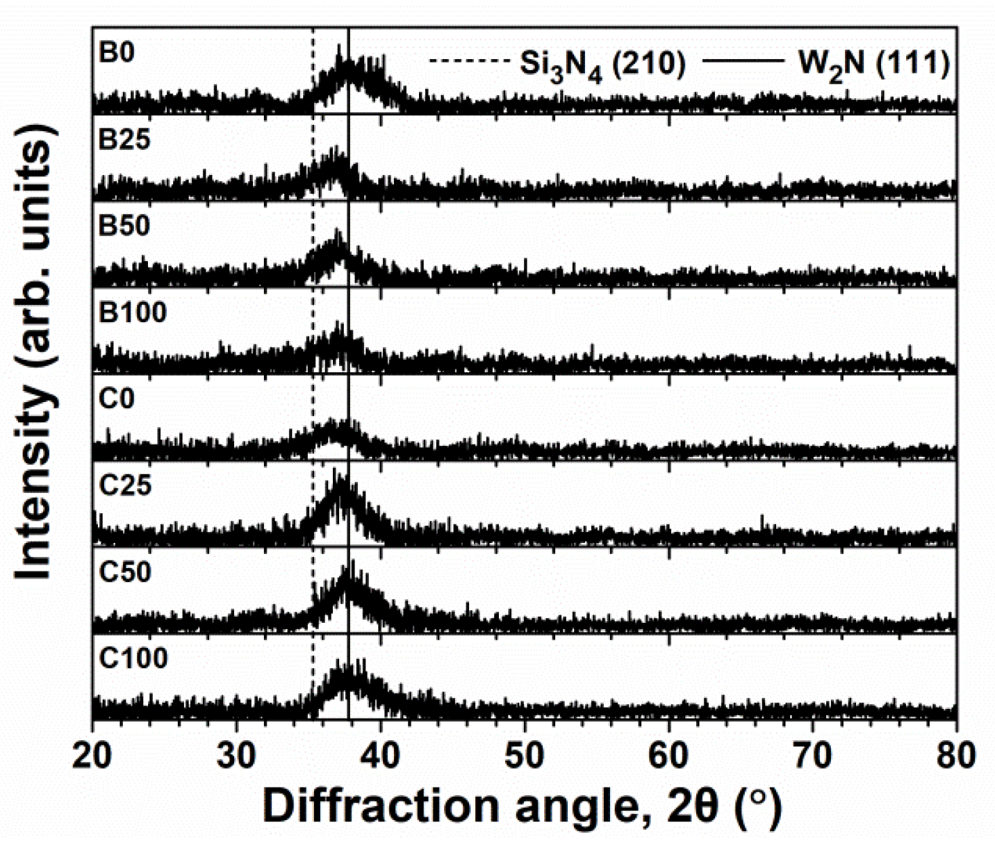
3.3. W–Si–N Films Prepared with Various Bias Voltages

Table 4 lists the atomic compositions and thicknesses of the W–Si–N films. The Batch B and C samples, with high Si concentrations of 13.5–16.5 and 27.0–30.9 at.%, respectively, exhibited near-amorphous XRD patterns (Figure 6) and low residual stresses of −0.6 to −0.9 and −0.5 to −0.7 GPa, respectively (Table 4). Studies [19,20,21,22] have reported that Si3N4 is more stable than W2N, WN, and W-silicide based on thermodynamic considerations. Therefore, excess N or Si atoms reacted with W after Si3N4 formation [20]. The high Si and low W concentrations indicate that Batch C samples were amorphous Si3N4-dominated films.
Table 5 displays the mechanical properties of W–Si–N films prepared using various substrate bias voltages. The X-ray amorphous films, Batches B and C, exhibited low H values of 17.1–22.3 GPa, low E values of 218–253 GPa, and low residual stresses, ranging from −0.5 to −0.9 GPa. Moreover, the H values of the Batch C samples were similar to the reported value of 19 GPa for SiNx films [48,49]. Crystalline films, W04, W05, and Batch A films with a W2N phase exhibited high H values of 25.9–31.5 GPa, high E values of 303–351 GPa, and high residual stresses, ranging from −1.6 to −3.2 GPa. Figure 7 summarizes the mechanical properties of the W–N and W–Si–N films relative to their residual stress. The mechanical properties of the W–Si–N and W–N films prepared with various powers, assessed in our previous work [13], are also presented for comparison. Figure 8 illustrates the relationship between H and E for the samples displayed in Figure 7. The amorphous films (Batches B and C) exhibited H/E levels of approximately 0.080 ± 0.004, whereas the crystalline W2N films exhibited high H/E values. The Ra values of these amorphous W–Si–N films were 2.10–4.00 nm, which was lower than those of the crystalline W–N films.

3.4. Wear Test

The wear resistance of W–N and W–Si–N films of various categorizations was examined. W01 was the crystalline W–N films with a W phase; W04, A50, and A100 were the crystalline W–N films with a W2N phase; B100 and C100 were the amorphous W–Si–N films. Figure 9 presents the coefficients of friction (COFs) of the samples against the cemented tungsten carbide ball after a sliding distance of 200 m. The relationship between COF and Ra was unclear, which can be attributed to the distinct categorizations of the tested films. Therefore, further research is warranted to investigate this relationship. The abrupt drops of COF in the W01 and C100 samples can be attributed to the exhaustion of films and exposure of the substrates. Table 6 summarizes the wear test results. The wear depths of the W01 and C100 samples were 1334 and 1404 nm, respectively, which were larger than their film thicknesses of 675 and 574 nm, respectively. The other samples exhibited wear depths that were smaller than their film thickness. Figure 10 illustrates the wear scars of the tested samples. Chipping debris was observed along the wear scar of the W01 samples (Figure 10a). The H/E and H3/E2 values of the W01 samples were 0.067 and 0.100, respectively, which were the lowest levels of the tested samples and indicated that W01 was brittle. The wear scars on the C100 samples displayed extrusions of fractured films on part of the wear track (Figure 10f). The wear track widths of the A50, A100, and W04(A0) samples were 89, 96, and 99 μm, respectively, which was narrow compared with the other tested samples and can be attributed to their high H values [50]. The wear rates of the A50 and A100 films were 1.0 × 10⁶ and 7.5 × 107 mm3/Nm, with respective low COFs of 0.49 and 0.46 and high H3/E2 values of 0.321 and 0.230. The amorphous B100 sample exhibited a smooth wear scar and a broad track width of 138 μm because of a low H (22.3 GPa) and a high wear rate (4.9 × 106 mm3/Nm).

4. Conclusions

The effects of the f and substrate bias on the mechanical properties of W–N and W–Si–N films were investigated. The main findings were as follows:
(1)
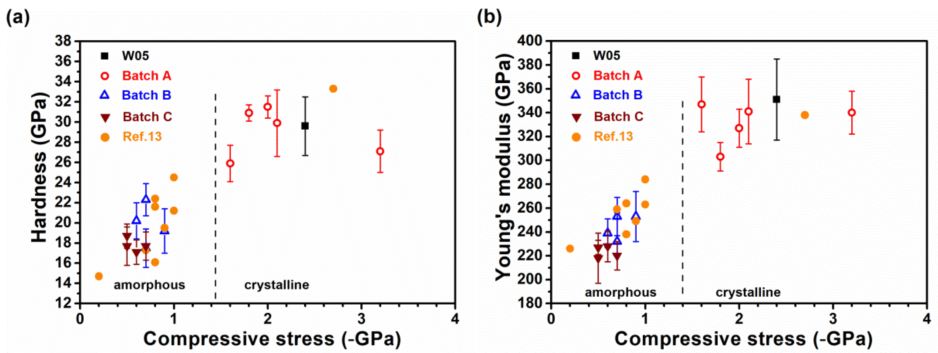
W–N films varied in phase from α-W to amorphous and β-W2N as f increased from 0.1 to 0.5, accompanied by increases in the compressive residual stress, H/E ratio, H3/E2 ratio, and elastic recovery (We).
(2)
W–N films fabricated with an f level of 0.4 and a negative substrate bias voltage of 0–150 V exhibited a β-W2N phase with a texture of (200). Films prepared with bias voltages in the range of −25 to −100 V exhibited high H levels of 29.9–31.5 GPa, low E levels of 303–341 GPa, high H/E ratios of 0.088–0.102, high H3/E2 ratios of 0.230–0.321 GPa, and high We values of 66%–67%.
(3)
The W–Si–N films with an Si concentration of 13.5–16.5 at.% displayed an amorphous structure. These films, prepared with negative substrate bias voltages of 0–100 V, exhibited limited deviation in residual stress (−0.6 to −0.9 GPa), with low H (17.5–22.3 GPa) and low E (232–253 GPa). Similar results were observed for the amorphous W–Si–N films with a Si concentration of 27.0–30.9 at.%, which behaved similarly to amorphous SiNx films in terms of residual stress (−0.5 to −0.7 GPa), H (17.1–18.7 GPa), and E (218–228 GPa). All of these mechanical properties were the lowest levels in this study.
(4)
The wear resistance of the W–N and W–Si–N films was examined using the pin-on-disk test method. The results indicated that the W–N films fabricated with an f level of 0.4 and negative substrate bias voltages of 50–100 V exhibited low wear rates of 7.5–10 × 107 mm3/Nm and low COFs of 0.46–0.49, with high H3/E2 ratios of 0.230–0.321 GPa.

Author Contributions

Conceptualization, L.-C.C. and Y.-I.C.; Formal analysis, M.-C.S. and Y.-I.C.; Investigation, M.-C.S. and L.-H.C.; Project administration, Y.-I.C.; Resources, L.-C.C. and Y.-I.C.; Validation, M.-C.S. and Y.-I.C.; Writing—original draft, Y.-I.C. All authors have read and agreed to the published version of the manuscript.

Funding

This research was funded by the Ministry of Science and Technology, Taiwan, grant number 106-2221-E-019-022-MY3.

Acknowledgments

The AES and FE-EPMA analyses in the Precision Instrument Center of National Tsing-Hua University are gratefully appreciated.

Conflicts of Interest

The authors declare no conflict of interest.

References

  1. Castanho, J.; Cavaleiro, A.; Vieira, M.T. Study of tungsten sputtered films with low nitrogen content. Vacuum 1994, 45, 1051–1053. [Google Scholar] [CrossRef]
  2. Hones, P.; Martin, N.; Regula, M.; Lévy, F. Structural and mechanical properties of chromium nitride, molybdenum nitride, and tungsten nitride thin films. J. Phys. D Appl. Phys. 2003, 36, 1023–1029. [Google Scholar] [CrossRef]
  3. Polcar, T.; Parreira, N.M.G.; Cavaleiro, A. Structural and tribological characterization of tungsten nitride coatings at elevated temperature. Wear 2008, 265, 319–326. [Google Scholar] [CrossRef]
  4. Samano, E.C.; Clemente, A.; Díaz, J.A.; Soto, G. Mechanical properties optimization of tungsten nitride thin films grown by reactive sputtering and laser ablation. Vacuum 2010, 85, 69–77. [Google Scholar] [CrossRef]
  5. Wen, M.; Meng, Q.N.; Yu, W.X.; Zheng, W.T.; Mao, S.X.; Hua, M.J. Growth, stress and hardness of reactively sputtered tungsten nitride thin films. Surf. Coat. Technol. 2010, 205, 1953–1961. [Google Scholar] [CrossRef]
  6. Chang, C.L.; Chiou, T.H.; Chen, P.H.; Chen, W.C.; Ho, C.T.; Wu, W.Y. Characteristics of TiN/W2N multilayers prepared using magnetron sputter deposition with dc and pulsed dc powers. Surf. Coat. Technol. 2016, 303, 25–31. [Google Scholar] [CrossRef]
  7. Lou, B.S.; Moirangthem, I.; Lee, J.W. Fabrication of tungsten nitride thin films by superimposed HiPIMS and MF system: Effects of nitrogen flow rate. Surf. Coat. Technol. 2020, 393, 125743. [Google Scholar] [CrossRef]
  8. Polcar, T.; Cavaleiro, A. Structure, mechanical properties and tribology of W–N and W–O coatings. Int. J. Refract. Met. Hard Mat. 2010, 28, 15–22. [Google Scholar] [CrossRef]
  9. Jiang, P.C.; Chen, J.S.; Lin, Y.K. Structural and electrical characteristics of W–N thin films prepared by reactive rf sputtering. J. Vac. Sci. Technol. A 2003, 21, 616–622. [Google Scholar] [CrossRef]
  10. Baker, C.C.; Shah, S.I. Reactive sputter deposition of tungsten nitride thin films. J. Vac. Sci. Technol. A 2002, 20, 1699–1703. [Google Scholar] [CrossRef]
  11. Wicher, B.; Chodun, R.; Nowakowska-Langier, K.; Trzcinski, M.; Skowroński, L.; Okrasa, S.; Minikayev, R.; Naparty, M.K.; Zdunek, K. Chemical and structural characterization of tungsten nitride (WNx) thin films synthesized via gas injection magnetron sputtering technique. Vacuum 2019, 165, 266–273. [Google Scholar] [CrossRef]
  12. Yamamoto, T.; Kawate, M.; Hasegawa, H.; Suzuki, T. Effects of nitrogen concentration on microstructures of WNX films synthesized by cathodic arc method. Surf. Coat. Technol. 2005, 193, 372–374. [Google Scholar] [CrossRef]
  13. Liu, Y.H.; Chang, L.C.; Liu, B.W.; Chen, Y.I. Mechanical properties and oxidation behavior of W–Si–N coatings. Surf. Coat. Technol. 2019, 375, 727–738. [Google Scholar] [CrossRef]
  14. Javdošňák, D.; Musil, J.; Soukup, Z.; Haviar, S.; Čerstvý, R.; Houska, J. Tribological properties and oxidation resistance of tungsten and tungsten nitride films at temperatures up to 500 °C. Tribol. Int. 2019, 132, 211–220. [Google Scholar] [CrossRef]
  15. Bielawski, M. Residual stress control in TiN/Si coatings deposited by unbalanced magnetron sputtering. Surf. Coat. Technol. 2006, 200, 3987–3995. [Google Scholar] [CrossRef]
  16. Tan, S.; Zhang, X.; Wu, X.; Fang, F.; Jiang, J. Effect of substrate bias and temperature on magnetron sputtered CrSiN films. Appl. Surf. Sci. 2011, 257, 1850–1853. [Google Scholar] [CrossRef]
  17. Guruvenket, S.; Rao, G.M. Bias induced structural changes in tungsten nitride films deposited by unbalanced magnetron sputtering. Mater. Sci. Eng. B 2004, 106, 172–176. [Google Scholar] [CrossRef]
  18. Louro, C.; Cavaleiro, A. Mechanical behaviour of amorphous W–Si–N sputtered films after thermal annealing at increasing temperatures. Surf. Coat. Technol. 2000, 123, 192–198. [Google Scholar] [CrossRef]
  19. Fu, T.; Zhou, Z.F.; Li, K.Y.; Shen, Y.G. Characterization of sputter deposited W–Si–N coatings based on α-W structure. Mater. Lett. 2005, 59, 618–623. [Google Scholar] [CrossRef]
  20. Musil, J.; Daniel, R.; Soldan, J.; Zeman, P. Properties of reactively sputtered W–Si–N films. Surf. Coat. Technol. 2006, 200, 3886–3895. [Google Scholar] [CrossRef]
  21. Ju, H.; He, S.; Yu, L.; Asempah, I.; Xu, J. The improvement of oxidation resistance, mechanical and tribological properties of W2N films by doping silicon. Surf. Coat. Technol. 2017, 317, 158–165. [Google Scholar] [CrossRef]
  22. Anwar, S.; Islam, A.; Anwar, S. Mechanical studies of thermally annealed nc-W2N embedded a-Si3N4 nanocomposite films. Thin Solid Film. 2017, 636, 93–98. [Google Scholar] [CrossRef]
  23. Zhao, H.; Ye, F. Effect of Si-incorporation on the structure, mechanical, tribological and corrosion properties of WSiN coatings. Appl. Surf. Sci. 2015, 256, 958–966. [Google Scholar] [CrossRef]
  24. Hong, T.E.; Jung, J.H.; Yeo, S.; Cheon, T.; Bae, S.I.; Kim, S.H.; Yeo, S.J.; Kim, H.S.; Chung, T.M.; Park, B.K.; et al. Highly conformal amorphous W−Si−N thin films by plasma-enhanced atomic layer deposition as a diffusion barrier for Cu metallization. J. Phys. Chem. C 2015, 119, 1548–1556. [Google Scholar] [CrossRef]
  25. Sandu, C.S.; Sanjinés, R.; Benkahoul, M.; Medjani, F.; Lévy, F. Formation of composite ternary nitride thin films by magnetron sputtering co-deposition. Surf. Coat. Technol. 2006, 201, 4083–4089. [Google Scholar] [CrossRef]
  26. Sundgren, J.-E.; Johansson, B.-O.; Hentzell, H.T.G.; Karlsson, S.-E. Mechanisms of reactive sputtering of titanium nitride and titanium carbide III: Influence of substrate bias on composition and structure. Thin Solid Film. 1983, 105, 385–393. [Google Scholar] [CrossRef]
  27. Petrov, I.; Hultman, L.; Helmersson, U.; Sundgren, J.-E.; Greene, J.E. Microstructure modification of TiN by ion bombardment during reactive sputter deposition. Thin Solid Film. 1989, 169, 299–314. [Google Scholar] [CrossRef]
  28. Lee, H.C.; Lee, J.Y.; Ahn, H.J. Effect of the substrate bias voltage on the crystallographic orientation of reactively sputtered AlN thin films. Thin Solid Film. 1994, 251, 136–140. [Google Scholar] [CrossRef]
  29. Yang, Z.T.; Yang, B.; Guo, L.P.; Fu, D.J. Effect of bias voltage on the structure and hardness of Ti–Si–N composite coatings synthesized by cathodic arc assisted middle-frequency magnetron sputtering. J. Alloy. Compd. 2009, 473, 437–441. [Google Scholar] [CrossRef]
  30. Chen, Y.I.; Zheng, Y.Z.; Chang, L.C.; Liu, Y.H. Effect of bias voltage on mechanical properties of HiPIMS/RFMS cosputtered Zr–Si–N films. Materials 2019, 12, 2658. [Google Scholar] [CrossRef] [Green Version]
  31. Cullity, B.D.; Stock, S.R. Elements of X-ray Diffraction, 3rd ed.; Prentice Hall: Upper Saddle River, NJ, USA, 2001. [Google Scholar]
  32. Jones, M.I.; McColl, I.R.; Grant, D.M. Effect of substrate preparation and deposition conditions on the preferred orientation of TiN coatings deposited by RF reactive sputtering. Surf. Coat. Technol. 2000, 132, 143–151. [Google Scholar] [CrossRef]
  33. Saha, R.; Nix, W.D. Effects of the substrate on the determination of thin film mechanical properties by nanoindentation. Acta Mater. 2002, 50, 23–38. [Google Scholar] [CrossRef]
  34. Oliver, W.C.; Pharr, G.M. An improved technique for determining hardness and elastic modulus using load and displacement sensing indentation experiments. J. Mater. Res. 1992, 7, 1564–1583. [Google Scholar] [CrossRef]
  35. Janssen, G.C.A.M.; Abdalla, M.M.; van Keulen, F.; Pujada, B.R.; van Venrooy, B. Celebrating the 100th anniversary of the Stoney equation for film stress: Developments from polycrystalline steel strips to single crystal silicon wafers. Thin Solid Film. 2009, 517, 1858–1867. [Google Scholar] [CrossRef]
  36. Chen, Y.I.; Ke, Y.E.; Sung, M.C.; Chang, L.C. Rapid thermal annealing of Cr–Si–N, Ta–Si–N, and Zr–Si–N coatings in glass molding atmospheres. Surf. Coat. Technol. 2020, 389, 125662. [Google Scholar] [CrossRef]
  37. Shen, Y.G.; Mai, Y.W.; McBride, W.E.; Zhang, Q.C.; McKenzie, D.R. Structural properties and nitrogen-loss characteristics in sputtered tungsten nitride films. Thin Solid Film. 2000, 372, 257–264. [Google Scholar] [CrossRef]
  38. Pogrebnjak, A.D.; Beresnev, V.M.; Bondar, O.V.; Postolnyi, B.O.; Zaleski, K.; Coy, E.; Jurga, S.; Lisovenko, M.O.; Konarski, P.; Rebouta, L.; et al. Superhard CrN/MoN coatings with multilayer architecture. Mater. Des. 2018, 153, 47–59. [Google Scholar] [CrossRef]
  39. Musil, J. Hard nanocomposite coatings: Thermal stability, oxidation resistance and toughness. Surf. Coat. Technol. 2012, 207, 50–65. [Google Scholar] [CrossRef]
  40. Tsui, T.Y.; Pharr, G.M.; Oliver, W.C.; Bhatia, C.S.; White, R.L.; Anders, S.; Anders, A.; Brown, I.G. Nanoindentation and nanoscratching of hard carbon coatings for magnetic disks. Mater. Res. Soc. Symp. Proc. 1995, 383, 447–452. [Google Scholar] [CrossRef] [Green Version]
  41. Musil, J.; Kunc, F.; Zeman, H.; Poláková, H. Relationships between hardness, Young′s modulus and elastic recovery in hard nanocomposite coatings. Surf. Coat. Technol. 2002, 154, 304–313. [Google Scholar] [CrossRef]
  42. Leyland, A.; Matthews, A. On the significance of the H/E ratio in wear control: A nanocomposite coating approach to optimised tribological behavior. Wear 2000, 246, 1–11. [Google Scholar] [CrossRef]
  43. Qasmi, M.; Delobelle, P. Influence of the average roughness Rms on the precision of the Young’s modulus and hardness determination using nanoindentation technique with a Berkovich indenter. Surf. Coat. Technol. 2007, 201, 1191–1199. [Google Scholar] [CrossRef]
  44. Walter, C.; Antretter, T.; Daniel, R.; Mitterer, C. Finite element simulation of the effect of surface roughness on nanoindentation of thin films with spherical indenters. Surf. Coat. Technol. 2007, 202, 1103–1107. [Google Scholar] [CrossRef]
  45. Walter, C.; Mitterer, C. 3D versus 2D finite element simulation of the effect of surface roughness on nanoindentation of hard coatings. Surf. Coat. Technol. 2009, 203, 3286–3290. [Google Scholar] [CrossRef]
  46. Qi, Z.B.; Sun, P.; Zhu, F.P.; Wang, Z.C.; Peng, D.L.; Wu, C.H. The inverse hall–petch effect in nanocrystalline ZrN coatings. Surf. Coat. Technol. 2011, 205, 3692–3697. [Google Scholar] [CrossRef]
  47. Mayrhofer, P.H.; Tischler, G.; Mitterer, C. Microstructure and mechanical/thermal properties of Cr–N coatings deposited by reactive unbalanced magnetron sputtering. Surf. Coat. Technol. 2001, 142–144, 78–84. [Google Scholar] [CrossRef]
  48. Chen, Y.H.; Guruz, M.; Chung, Y.W.; Keer, L.M. Thermal stability of hard TiN/SiNx multilayer coatings with an equiaxed microstructure. Surf. Coat. Technol. 2002, 154, 162–166. [Google Scholar] [CrossRef]
  49. Abadias, G.; Uglov, V.V.; Saladukhin, I.A.; Zlotski, S.V.; Tolmachova, G.; Dub, S.N.; Janse van Vuuren, A. Growth, structural and mechanical properties of magnetron-sputtered ZrN/SiNx nanolaminated coatings. Surf. Coat. Technol. 2016, 308, 158–167. [Google Scholar] [CrossRef]
  50. Liu, K.Y.; Lee, J.W.; Wu, F.B. Fabrication and tribological behavior of sputtering TaN coatings. Surf. Coat. Technol. 2014, 259, 123–128. [Google Scholar] [CrossRef]
Figure 1. (a) Grazing incident and (b) Bragg–Brentano scan X-ray diffraction (XRD) patterns of the W–N films prepared using various N2 flow ratios (f).
Coatings 10 01252 g001
Figure 2. X-ray photoelectron spectroscopy (XPS) signals of (a) N 1s and (b) W 4f of Batch W films.
Coatings 10 01252 g002
Figure 3. (a) Grazing incident and (b) Bragg–Brentano scan XRD patterns of the Batch A films.
Coatings 10 01252 g003
Figure 4. Lattice parameter determinations of the Batch A films.
Coatings 10 01252 g004
Figure 5. Texture coefficients of the W05 and Batch A samples.
Coatings 10 01252 g005
Figure 6. Grazing incident X-ray diffraction (GIXRD) patterns of W–Si–N films.
Coatings 10 01252 g006
Figure 7. Relationships between (a) H and (b) E and residual stress of W–N and W–Si–N films.
Coatings 10 01252 g007
Figure 8. Relationship between H and E of the W–N and W–Si–N films.
Coatings 10 01252 g008
Figure 9. The coefficient of friction of the W–N and W–Si–N films.
Coatings 10 01252 g009
Figure 10. Wear scars of the (a) W01, (b) W04, (c) A50, (d) A100, (e) B100, and (f) C100 films.
Coatings 10 01252 g010
Table 1. Atomic compositions, thicknesses, and residual stresses of W–N films prepared using various N2 flow ratios and bias voltages.
SamplefaBiasAtomic Composition (at.%)RatioTbDcStress
(−V)WSiNON/W(nm)(nm/min)(GPa)
W010.1093.6 ± 0.80.7 ± 0.14.7 ± 0.21.0 ± 0.80.056758.40.0 ± 0.2
W020.2085.9 ± 1.41.9 ± 2.38.3 ± 2.23.9 ± 1.50.106187.7−0.7 ± 0.2
W030.3080.5 ± 3.11.7 ± 2.112.4 ± 2.85.4 ± 0.90.155687.1−1.4 ± 0.2
W04(A0)0.4075.4 ± 0.70.5 ± 0.022.5 ± 0.61.6 ± 0.40.305827.3−1.6 ± 0.2
W050.5072.8 ± 3.81.7 ± 2.025.3 ± 4.30.2 ± 0.40.355116.4−2.4 ± 0.2
A250.42572.8 ± 0.50.9 ± 0.125.5 ± 0.80.8 ± 0.30.356107.6−2.0 ± 0.2
A500.45074.1 ± 0.00.7 ± 0.023.6 ± 0.41.6 ± 0.30.325627.0−1.8 ± 0.3
A1000.410070.5 ± 2.42.0 ± 2.126.9 ± 0.90.6 ± 0.10.385446.8−2.1 ± 0.1
A1500.415066.3 ± 0.33.9 ± 0.229.1 ± 0.60.7 ± 0.60.445216.5−3.2 ± 0.8
af: N2 flow ratio; b T: thickness; c D: deposition rate.
Table 2. XPS analysis results of W–N films at depths of 27, 36, 45, and 54 nm.
SampleW 4f7/2
(eV)
W 4f7/2
(eV)
W 5p3/2 (eV)N 1s
(eV)
Intensity Ratio
W–WW–NN–WW–W:W–N
W0131.13 ± 0.0132.25 ± 0.0436.52 ± 0.04397.58 ± 0.1684:16
W0231.37 ± 0.0132.03 ± 0.0736.62 ± 0.03397.70 ± 0.0575:25
W0331.34 ± 0.0432.05 ± 0.0936.64 ± 0.06397.63 ± 0.0374:26
W04(A0)31.13 ± 0.0131.91 ± 0.0836.51 ± 0.04397.52 ± 0.0272:28
W0531.20 ± 0.0132.04 ± 0.0136.60 ± 0.02397.56 ± 0.0370:30
A2531.45 ± 0.0032.44 ± 0.0136.90 ± 0.03397.72 ± 0.0480:20
A5031.33 ± 0.0132.62 ± 0.0236.85 ± 0.01397.57 ± 0.0289:11
A10031.12 ± 0.0132.52 ± 0.0336.66 ± 0.01397.39 ± 0.0588:12
A15031.08 ± 0.0132.02 ± 0.0336.54 ± 0.02397.40 ± 0.0476:24
Table 3. Mechanical properties of W–N films.
SampleStressHaEbH/EH3/E2We cRad
(GPa)(GPa)(GPa)(GPa)(%)(nm)
W010.0 ± 0.222.4 ± 3.6335 ± 410.0670.100534.25 ± 0.06
W02−0.7 ± 0.226.2 ± 1.8388 ± 320.0680.1195613.23 ± 0.24
W03−1.4 ± 0.222.1 ± 0.9308 ± 140.0720.114603.09 ± 0.04
W04(A0)−1.6 ± 0.225.9 ± 1.8347 ± 230.0750.144603.42 ± 0.07
W05−2.4 ± 0.229.6 ± 2.9351 ± 340.0840.211634.54 ± 0.13
A25−2.0 ± 0.231.5 ± 1.1327 ± 160.0960.292673.10 ± 0.11
A50−1.8 ± 0.330.9 ± 0.8303 ± 120.1020.321664.93 ± 0.09
A100−2.1 ± 0.129.9 ± 3.3341 ± 270.0880.230674.12 ± 0.05
A150−3.2 ± 0.827.1 ± 2.1340 ± 180.0800.172613.95 ± 0.07
aH: Hardness; bE: Young’s modulus; cWe: Elastic recovery; dRa: Average surface roughness.
Table 4. Atomic compositions, thicknesses, and residual stresses of W–Si–N films prepared using various bias voltages.
SampleBiasAtomic Composition (at.%)TaDbStress
(−V)WSiNO(nm)(nm/min)(GPa)
PWc = 150 W, PSi d = 150 W
B0046.9 ± 0.716.5 ± 0.134.0 ± 0.72.6 ± 0.164610.8−0.9 ± 0.2
B252546.7 ± 0.914.9 ± 0.237.4 ± 1.01.0 ± 0.260810.1−0.7 ± 0.2
B505039.9 ± 0.513.5 ± 0.146.0 ± 0.50.6 ± 0.271211.9−0.6 ± 0.2
B10010047.1 ± 0.115.3 ± 0.235.8 ± 0.21.8 ± 0.263410.6−0.7 ± 0.2
PW = 60 W, PSi = 150 W
C0025.9 ± 0.427.0 ± 0.045.5 ± 0.51.6 ± 0.65497.3−0.6 ± 0.1
C252522.0 ± 0.330.0 ± 0.147.7 ± 0.20.3 ± 0.25427.2−0.5 ± 0.2
C505024.8 ± 0.328.5 ± 0.246.3 ± 0.40.4 ± 0.45457.3−0.7 ± 0.1
C10010020.4 ± 0.530.9 ± 0.248.3 ± 0.60.4 ± 0.15747.7−0.5 ± 0.1
aT: thickness; bD: deposition rate; cPW: power on W target; dPSi: power on Si target.
Table 5. Mechanical properties of W–Si–N films.
SampleStressHaEbH/EH3/E2We cRad
(GPa)(GPa)(GPa)(GPa)(%)(nm)
B0−0.9 ± 0.219.2 ± 2.2253 ± 210.0760.111663.65 ± 0.01
B25−0.7 ± 0.217.5 ± 1.9232 ± 240.0760.100604.00 ± 0.04
B50−0.6 ± 0.220.2 ± 1.8239 ± 120.0840.144602.10 ± 0.05
B100−0.7 ± 0.222.3 ± 1.6253 ± 160.0880.173602.35 ± 0.07
C0−0.6 ± 0.117.1 ± 1.2228 ± 130.0750.096642.37 ± 0.06
C25−0.5 ± 0.218.7 ± 1.2227 ± 60.0830.127572.85 ± 0.05
C50−0.7 ± 0.117.7 ± 1.4220 ± 120.0800.115582.65 ± 0.02
C100−0.5 ± 0.117.7 ± 1.9218 ± 210.0810.117593.06 ± 0.09
aH: Hardness. bE: Young’s modulus. cWe: Elastic recovery; dRa: Average surface roughness.
Table 6. Wear test results of the W–N and W–Si–N films.
SampleThicknessWear Depth aWidth aμ bWear RateH3/E2Rac
(nm)(nm)(μm)(mm3/Nm)(GPa)(nm)
W0167513341560.522.4 × 10−50.1004.25
W04(A0)582341990.601.8 × 10−60.1443.42
A50636218890.491.0 × 10−60.3214.93
A100574208960.467.5 × 10−70.2304.12
B1006343191380.554.9 × 10−60.1732.35
C10057414041150.655.6 × 10−60.1173.06
a Width: Wear track width. b μ: Coefficient of friction; c Ra: Average surface roughness.
Publisher’s Note: MDPI stays neutral with regard to jurisdictional claims in published maps and institutional affiliations.

