Review

Preparation and Characterization of NbxOy Thin Films: A Review

by
Nwanna Charles Emeka
,
Patrick Ehi Imoisili
and
Tien-Chien Jen
*
Department of Mechanical Engineering Science, Faculty of Engineering and the Built Environment, University of Johannesburg, Auckland, Johannesburg 2006, South Africa
*
Author to whom correspondence should be addressed.
Coatings 2020, 10(12), 1246; https://doi.org/10.3390/coatings10121246
Submission received: 5 November 2020 / Revised: 9 December 2020 / Accepted: 13 December 2020 / Published: 17 December 2020
(This article belongs to the Special Issue Metal Oxide Films and Their Applications)

Abstract

:
Niobium oxides (NbO, NbO2, Nb2O5), being a versatile material has achieved tremendous popularity to be used in a number of applications because of its outstanding electrical, mechanical, chemical, and magnetic properties. NbxOy films possess a direct band gap within the ranges of 3.2–4.0 eV, with these films having utility in different applications which include; optical systems, stainless steel, ceramics, solar cells, electrochromic devices, capacitor dielectrics, catalysts, sensors, and architectural requirements. With the purpose of fulfilling the requirements of a vast variety of the named applications, thin films having comprehensive properties span described by film composition, morphology, structural properties, and thickness are needed. The theory, alongside the research status of the different fabrication techniques of NbxOy thin films are reported in this work. The impact of fabrication procedures on the thin film characteristics which include; film thickness, surface quality, optical properties, interface properties, film growth, and crystal phase is explored with emphases on the distinct deposition process applied, are also described and discussed.

1. Introduction

Niobium, a chemical substance having a symbol of Nb, is a ductile transition metal which is light grey in colour with a crystalline structure [1]. Nobium, also is known as columbium and titanium in their pure states, possess similar hardness [2], as well as a ductility comparable to that of iron. Niobium can often be discovered in pyrochlore and columbite minerals, resulting in its previous name of “columbium”. The oxidation of niobium in the earth’s atmosphere is extremely slow, thus its utilization in jewellery as a hypoallergenic substitute to nickel [3]. Niobium alongside its oxides are crucial and strategically high materials of technology. Niobium oxides bring about several diverse and remarkable properties, ranging from its solid appearance in nature, to its, melting point of 1512 °C, its insolubility in water but solubility in hydrogen fluorides (HF), its density and molecular weight of 4.47 g/cm3 and 265.81. All these to a large extent, make it a flexible group of material. Precisely, niobium oxides have shown enormous potentials in numerous applications of technology which include, transparent conductive oxides, solid electrolytic capacitors, photochromic devices, dye-sensitized solar cells and memristors.
Niobium oxides which are n-type semiconductors are inclusive of, but not limited to; niobium dioxide (niobium (IV) oxide) NbO2, niobium monoxide (niobium (II) oxide) NbO, niobium pentoxide (niobium (V) oxide) Nb2O5, as there are other different oxides of the metal. Each of these oxides of niobium have distinct electrical characteristics which ranges from metallic conducting NbO to semiconducting NbO2 with κ (kappa) value of 3.9 [4], and then insulating Nb2O5 [5], which thermodynamically, is the most stable oxide, with the smallest available energy formation [6,7]. However, the existence of NbO and NbO2 in a film, would influence the general properties of the Nb2O5 films [8]. Niobium pentoxide (Nb2O5) is consistently formed when sufficient oxygen is supplied during the reaction process. Nevertheless, when other oxides of niobium are required, there should be a limitation to the quantity of oxygen supplied to avoid the production of Nb2O5. The difficulty here is in discovering the appropriate amount of oxygen flow rate needed to attain the needed stoichiometry [9]. A study, which was performed by Venkataraj et al. [10], stated that an oxygen flow rate beyond 7 sccm was adequate for the formation of the pentoxide film, though no report was made on the fabrication of the other oxide films. However, the system of niobium−oxygen is remarkably a complicated one, because very little deviations in the precise stoichiometry of Nb2O5 greatly influences the material’s physical properties. For example, with little deficiency in oxygen, the Nb2O5 transits from insulating to n-type semiconducting properties [11].
The finding of electrochromism by Reichman and Bard from Nb2O5 in the year 1980 [12], resulted in the oxide being comprehensively researched after being discovered as an encouraging electrochromic material for its application in devices due to its exceptional chemical stability as well as corrosive resistivity in both acid and base forms. This electrochromism is an occurrence in relation to a continuous and reversible optical change generated electrochemically, of which its macroscopic effect is a colour change [13]. Thin films of niobium oxide exhibit transparent to brownish, grey or blue electrochromism with the introduction of ions like Li+ or H+, and this alters the optical transmittance to 24% from an initial 78% (l ¼ 600 nm) with a colouring or bleaching kinetic of about 10 s. However, the standard of an electrochromic material is measured based on its coloration efficiency, which is its contrast in transmittance between the coloured or bleached states as a result of the injected charge, the time of response, and the chemical stability. Consequently, these features are contingent on the Nb2O5 film’s material characteristics. [14]. One of the advantages of Nb2O5 films over tungsten oxide is this ability of it being able to obtain various colours, ranging between brown amorphous layers to blue crystalline layers [15]. Therefore, based on its crystalline nature, the transparent Nb2O5 thin film in its reduced state shows distinct colours of blue, brown or grey [16].
The similarities between the properties of microscopic and macroscopic materials, as well as their deposition variables, provides very essential guidance and direction towards the optimization of materials for different applications. This particularly, is typical of oxides of niobium, as films of niobium oxides display varying electrical and optical features as a result of their deposition techniques and production parameters [17]. Niobium oxide films have been suggested to be used in a vast array of technical applications, which include, sensing materials [18,19,20], assisting with the process of catalysis [21,22,23], and for use as biocompatible coatings [24,25,26]. Niobium (V) oxide (Nb2O5) which possesses a high dielectric constant and a high refractive index of 200 and 2.4 respectively, with also a broad band gap of 3.2–4.0 eV, can be employed in many different applications like; electrochromic devices, capacitor dielectrics, oxygen sensors, solar cells and catalysts [27,28,29]. Niobium pentoxide which is a transparent dielectric material is a perfect material for use in the development of capacitors, and in the application of optical systems [30]. As a result of its higher permittivity in contrast to that of Ta2O5, it has been proposed as a logical alternative for Ta2O5 in the application of capacitors of solid electrolyte tantalum/tantalum pentoxide (Ta2O5) [31], in which the dielectric layer of the oxide is produced via a porous metal powder compressed by anodic oxidation. This is because, not only does it have comparable anodization characteristics to Ta2O5 but also offers the benefit of more abundance in the nature, thus the reduction in price of raw materials [32,33,34]. Also, a comprehensive study has been performed on the pentoxide labelling it as gate dielectrics in complementary metal oxide semiconductors (CMOS) components [35] which as well displays exceptional catalytic qualities. High-κ (kappa) Nb2O5 can be used as a substitute to the traditional gate dielectric of SiO2 [3,9], so as to satisfy the requirements for miniaturization of the dynamic random-access memory along with the complementary metal oxide semiconductor components [36,37]. The composition of the Nb2O5 films is literally affected by the partial pressure of oxygen and the deposition temperature which may probably lead to an alternation in the dielectric constant [38]. Latest reports have included the incorporation of Nb2O5 in electrode materials of electrochemical applications, and this has brought about outstanding performance which is largely attributed to the intercalation pseudo-capacitance effect of the doped Li+ [7,39,40]. Niobium monoxide which is a metallic material has a superconductivity at 1.38 K [41], thus, is being utilized in superconducting circuits as a resistor [42].
Niobium dioxide itself is a semiconductor which has exceptional field-switching qualities [43], and has proved itself as an encouraging assistance for platinum in the oxidation of methanol as well as a reducing agent in fuel cell technologies [44]. Niobium dioxide experiences a transition from metal to insulator with drastic transformations in resistivity and magnetic sensitivity, as well as a concurrent structural transformation to a rutile structure from a rutile twisted structure [45]. NbO2′s transition characteristics have so much similarity with those of Vanadium dioxide (VO2) [46]. However, NbO2′s transition temperature is far greater than VO2′s, (approximately 340 K), making it less vulnerable to Joule heating and thus more attractive in circuit applications. It is stated that the metal insulator transition (MIT) in NbO2 could also be activated by an applied electrical field [47,48], thus making it appealing for use as a switching material which can possibly be utilized as nanoelectronic devices [47]. Regardless of the NbO2′s desirable features, experimental works on NbO2 thin films have been minimal as a result of the challenges faced in the production of NbO2 films of high quality. Its production is difficult since Nb4+ does not exist as a stable niobium oxidation state and thus is easily over-oxidized [49]. Previous works indicated that amorphous and polycrystalline films of NbO2 were formed by sputtering an NbO2 material from the reduction of Nb2O5 through the chemical vapour transport method [50].
Due to its high electrical properties, niobium oxide has been employed as a dopant for a number of materials such as tin, vanadium, lead, tungsten, titanium, bismuth and zinc. However, one problem with niobium oxide is its complex crystal system which consists of a wide variation of polymorphic forms [51], even though these polymorphic forms brings about interesting successions with regards to structural phases. These phases are usually determined by the NbO6 octahedral groups, which form different arrangements from the rectangular block of columns. The most frequently identified phases were termed H, M, T, B and TT, with their occurrences resting on the techniques and conditions used in preparation. For example, the most thermodynamically stable is the H-phase [52], and it is the one produced at temperatures beyond 1000 °C. The other phases of T [53] and TT [54,55] acquire stability at temperatures ranging between 650–800 °C and 300–550 °C respectively. Nb2O5 has a wide range of features, based on their crystalline modifications. The H-phase has a high dielectric constant of approximately 100 [56], the T-phase is highly electrochemically stable with an outstanding cycling performance [57], while the electrochromic devices are especially interested in the TT-phase.
Many different effective deposition procedures have been implemented for the production of the thin films of Nb2O5, which consists of, sol gel process [58], chemical spray pyrolysis [16], sputtering [14], pulsed laser deposition [18], biased target ion beam deposition [49] electron beam evaporation [59], electrochemical deposition process [60], chemical vapour deposition (CVD) [17] and atomic layer deposition (ALD) [61].

2. Properties of Niobium Oxide Thin Films

2.1. Surface Morphology

The translucent niobium oxide solid material which is insoluble in water is stable in air, possessing a fairly complex structure that exhibits substantial polymorphism [62,63]. Nb2O5 has about 15 polymorphic forms which have been recorded hitherto. As shown in Table 1 and Figure 1, Monoclinic (H-Nb2O5), pseudohexagonal (TT-Nb2O5) and orthorhombic (T-Nb2O5) are typically the predominant crystal structures [64,65,66]. Amorphous NbO is usually attained after a low temperature deposition process, which afterwards crystallizes to TT or T phases at a temperature of 500 °C. Then at a medium temperature of 800 °C, it changes to the tetragonal M phase, which subsequently develops into the H phase at a temperature higher than 1000 [63,67]. Irrespective of the overall temperature influence, the preparation technique, the type of starting material, and the existence of contaminants alongside other interactions play a crucial part in the production of the resultant Nb2O5 crystal [66,67]. The best thermodynamically stabilized crystal phase is H-Nb2O5 and it is often formed once subjected to heat at temperatures beyond 1000 °C, whereas the forms of TT and M-Nb2O5 are often metastable [68].

2.2. Electrical Qualities

Niobium oxide (Nb2O5) is an n-type semiconductor of wide band gap. It possesses a conduction band which comprises of vacant Nb5+ 4d orbitals and possess a 0.2–0.4 eV conduction band value which is greater than that of titanium dioxide [76]. The band gap energy of niobium oxide has been described to be within the ranges of 3.1 to 5.3 eV (semiconductor to insulator with conductivity) [77]. However, it is feasible to adjust the of niobium oxide (Nb2O5) band gap and variables like stoichiometry, heat treatment, crystallinity, and integrated external ions may be able to unusually impact the band gap energy. Prior literatures have additionally disclosed that reducing the niobium oxide (Nb2O5) dimensions to nanoscale causes a blue shift in the energy gap, and this could be ascribed to the quantum size effect [63,78]. Importantly, nanostructure niobium oxide (Nb2O5) possesses particle sizes which could have a huge effect on the material’s electronic structure [79]. The difference of 0.25 eV between them is as a result of the blue shift of the porous nanotubes’ absorption edge. This is relative to the solid nanorods in respect to the quantum-size effect in the hollow nanotubes of Nb2O5 [80]. In some semiconductors, the amount of charge carriers in Nb2O5 is tied directly to the faulty metal oxide structure, which is temperature and oxygen pressure dependent.
In one of Le Viet et al. [64] studies, he experimentally investigated the crystalline Nb2O5 nanofibers band gap (hexagonal, orthorhombic and monoclinic) which were sintered at three distinct temperatures of 1100, 500 and 800. With reference to the Tauc plots which was obtained from the absorption spectra in Figure 2, they made a discovery that the orthorhombic (O-Nb2O5), monoclinic (M-Nb2O5), and hexagonal (H-Nb2O5) Nb2O5 structures all showed band gaps of 3.77, 3.79, and 3.85 eV respectively. Greener et al., studied the electrical conductivity of α-Nb2O5 monocrystalline and sintered specimens, under a constant ambient oxygen pressure and over the temperature range of 300 to 900 °C, and reported that they exhibit an exponential temperature dependence with an activation energy of 1.65 ev (Figure 3) [81].

2.3. Optical Features

The optical features of Nb2O5 have been experimentally examined by several techniques which are inclusive of spectrophotometry and spectroscopic ellipsometry [82,83]. Within the presence of H+ and Li+ ions intercalating ions, Nb2O5 has been proclaimed to be worthy of reversible and quick coloration. This trend is stated to be capable of modulating the transmission of optical Nb2O5 from a quasi-transparent phase (T ~ 85%) to below T ~ 10% in the visible or near infrared (IR) spectrum, and the ultraviolet (UV), and based on the nature of the film’s crystallinity, may display either of a blue or brown complexion [63,84,85]. As shown in Figure 4, Figure 5 and Figure 6, Nb2O5 can effectively absorb light within the near UV regions and the UV regions of the spectrum based on its crystallinity and film structure or can as well be utilized as a UV-light transparent material. It has been recorded that the refractive index of Nb2O5 films is in the range of 2 to 2.3 [86], with the film’s crystallinity making an important difference towards the material’s refractive index while decreasing from 2.30 to 2.20, after heat treating to 700 °C from room temperature [87].

2.4. Mechanical Properties

The mechanical features of Nb2O5 are of great significance in the manufacture of electronic appliances, particularly in the production of actuators and flexible mechanical components, for example micro-electro-mechanical devices. A bending analysis is vital for flexible device applications so as to control the stretching effects on the performance of the device and ensure that all element layers are secure after numerous thousands of flexes [63]. Stress as well as strain usually exists in thin films as a result of the deposition method or the limitations the substrate has been subjected to. Young’s modulus (Er) and average hardness (H) values for Nb2O5 deposited films are identified to be within the ranges of 117 to 268 Gpa and 5.6 to 6.8 Gpa, which again is affected by the crystal phase [87,91]. One of the most popular bending test methods which is a collapsing radius test was utilized in MIM capacitors for sputtered Nb2O5 thin films, and the data collected indicated tolerance of about 2500 flexes [63].

3. Methods of Deposition

The deposition of NbxOy thin films can be carried out via different techniques. This section analyzes and addresses the various fabrication methods and reaction systems towards the production of niobium oxide thin films. The different deposition processes are faced with different challenges which hinder the production of high-performance niobium oxide thin films. These challenges range from; the operating conditions of the process, the presence of impurities, nanoparticles resulting from homogeneous reactions, nature of precursor, type of solvent, slow deposition rates, to mention but a few. Nevertheless, additional information on each of the deposition procedures as well as the Biocompatibility of niobium oxide coatings can be found in the Supplementary Materials of this study.

3.1. Sol Gel

The sol-gel technique, as displayed in Figure 7A, is a low temperature process which has been broadly studied in different fields of technical and engineering applications to produce metal oxide nanostructures. It is a process in which small molecules are used to produce solid materials. This approach is utilized for manufacturing metal oxides of various kinds. Several studies have been conducted with regards to the production of thin films of niobium oxide. Inclusive, is the characterization of the sol-gel manufactured niobium pentoxide thin films to be used in electrochromic devices by Nilgun et al. [92]. They reported that the films after being cycled in a solution of propylene carbonate (PC) of 1 M LiCIO4, showed electrochromic properties after the electrochemical insertion (reduction), along with the extraction (oxidation) of lithium. The films of niobium pentoxide which indicated reversible optical switching between 320 and 870 nm, however, were discovered to be electrochromically passive at the infrared region. The authors stated that the surface analysis test with the use of the X-ray photoelectron spectroscopy (XPS) revealed minimal variation in the chemistry of the as-deposited Nb2O5 films. However, the reason for this minimal variation was not stated. These films were amorphous when characterized through the X-ray diffraction (XRD) process. Nilgun and Co. explained that the measurements of the optical transmittance in combination with the cyclic voltammograms, alongside the XPS spectra, disclosed the electrochromic behaviour of the films to have occurred as a result of inserting the Li + cations inside the niobium pentoxide films.
In a different study by Macek and Orel [58], they investigated the electromorphic sol-gel derived niobium oxide film. The structure of the xerogels, oxide powders and the equivalent films were analysed with the use of X-ray diffraction (XRD) together with the Fourier transform infrared (FT-IR) spectroscopic measurements. The authors explained that the electrochromic characteristics for the heat-treated crystalline films were conspicuous at 500 °C and showed a 60 percent transmittance adjustment (TA) in the ultraviolet (UV) and an 80% TA in the visible (VIS), in addition to a near-infrared (NIR) region between the coloured and bleached states respectively. Enhanced bleaching as well as increased reversible electrochromism of the thick films of niobium oxide of thickness greater than 250 nm, were acquired through lithiation. Macek and Orel also reported that electrochromic (EC) devices were further prepared through the assembly of an NbxOy film as well as a lithiated niobium oxide film with varying thickness, amidst a hybrid inorganic/organic Li+ ionic conductor (organically modified electrolyte-ormolyte) and a molybdenum and antimony doped tin oxide (SnO2: Sb (7%): Mo (10%)) counter electrode films. It was revealed that the EC devices displayed appropriate colouring/bleaching kinetics of less than 2 min, with colouring/bleaching transformations of around 40–50%.
The sol-gel technique acquires the following benefits over other deposition methods for Nb as stated in Table 2; ability to deposit on distinct surfaces, has a straightforward deposition process, requires no expensive equipment. The sol gel process is relatively less expensive compared to other deposition methods and it needs only minimal energy consumption. However, the sol gel technique acquires the disadvantages of being moisture sensitive, high cost of precursors, coupled with the tendency of its wet gel shrinking when dried [93,94,95,96].

3.2. Chemical Spray Pyrolysis
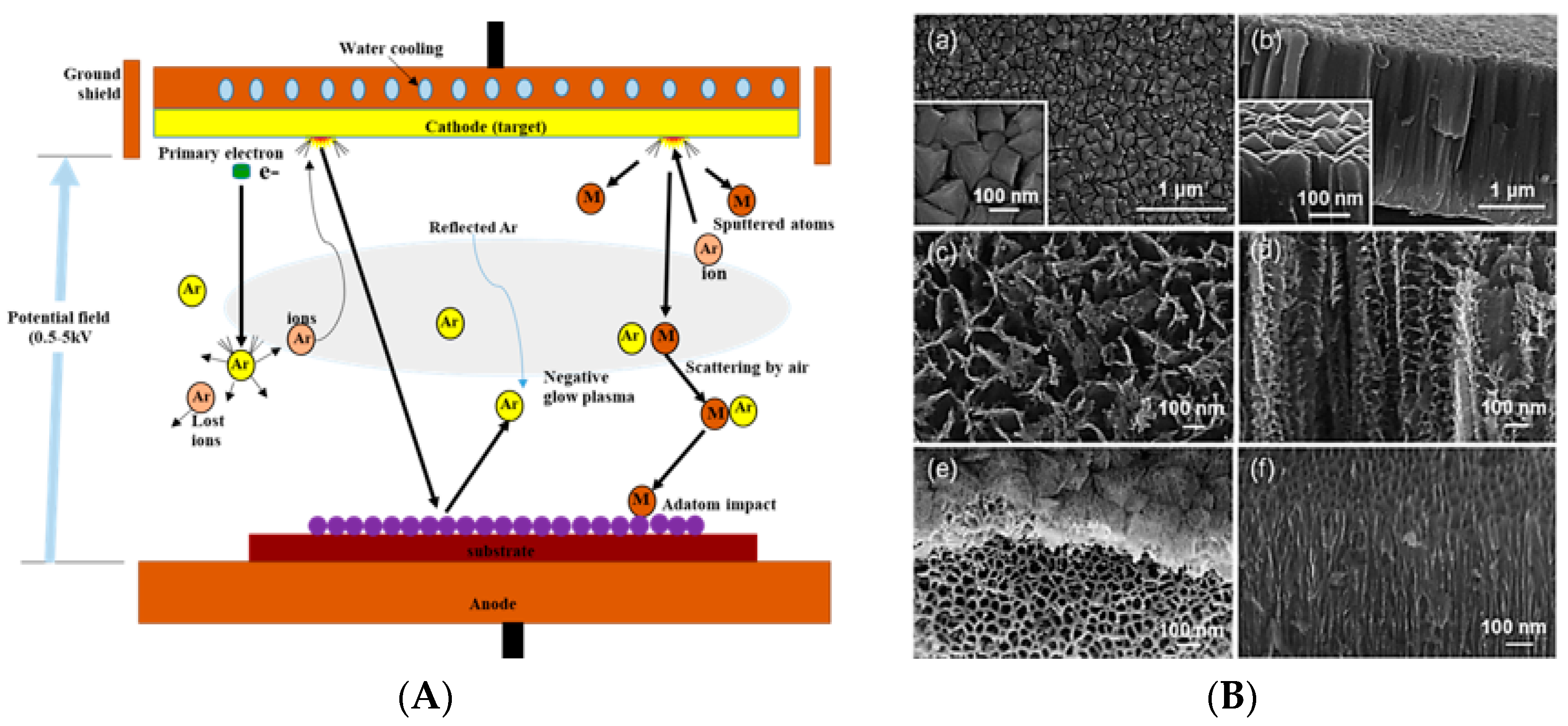
This is a process whereby a nanostructure is derived when the precursor already dissolved in a solution of the solvent is either sprayed or injected at ambient atmosphere, into extremely fine droplets of 1–2 μm by making use of high air pressure stream with the aid of a nanoporous nebulizer on the heated substrate in the furnace. This thus, brings about pyrolysis/decomposing of the precursor for the formation of the desired end product on the substrate as demonstrated in Figure 8A. [98]. There exist numerous studies for manufacturing niobium oxide films using the spray pyrolysis approach. One of these studies is the deposition of thin films of Nb2O5 through chemical spray pyrolysis performed by Romero et al. [99]. SEM and XPS analysis were carried out on the films to determine the surface structure and chemical composition of the film. The authors reported that the Nb2O5 thin films which were prepared from a precursor solution of 10−2 M NbCl5 on fused silica and glass substrates, possessed compact material with excessive surface roughness. However, the surface texture of the film decreased with increasing substrate temperature between 350 °C to 500 °C as the deposition velocity decreased. It was observed that all the as-deposited films possessed an amorphous structure, but there was no detailed explanation for this observation. Romero and Co. also revealed that post-annealing the films in air to temperatures above 500 °C lead to a twisted hexagonal crystal phase.
In another study, Romero et al. [100], investigated the electrochromic behaviour of thin films of Nb2O5 with distinct morphologies. Two varying procedures (single precursor solution injection and dual precursors solution injection) were used for the stabilization of the NbCl5 precursor to attain thin films of Nb2O5 by the spray pyrolysis process. With respect to the SEM analysis (Figure 8B), Romero and Co. explained that thin films of niobium oxide with distinct surface morphologies can be attained based on the procedure applied during the process. This can be determined by the manner of injection of the precursor solution into the airstream of the spray nozzle. From the XRD analysis, they reported the structural qualities of the Nb2O5 thin films to be dependent on the temperature of post-annealing, since the as-deposited films were amorphous irrespective of the type of synthesis process utilized. The authors stated that the electrochromic properties which were estimated for all the films, revealed that a 25.5 cm2/C monochromatic colouration efficiency, together with a cathodic charge density of about 24 mC/cm2, were discovered to produce optimum results for the thin films of niobium oxide achieved by the spray pyrolysis process. Chemical spray pyrolysis method possesses the merits of materials being easily doped, increase in film growth, and the final product possessing chemical homogeneity. The drawbacks of this method include, challenges in scaling up, excessive low yield, and the possibility of the sulphides oxidizing when being processed in air [98,99,101,102].

3.3. Sputtering

As demonstrated in Figure 9A, the sputtering method includes the ejection of a material from a target source onto a “substrate” for example, a silicon wafer. There are numerous sputtering processes, which include magnetron, diode, and ion beam sputtering. However, the most popular approach for the growth of thin films through the sputtering deposition process is via a magnetron source, whereby positive ions present in the plasma of a developed magnetic glow discharge, bombards the target [103]. Several works have been implemented with the use of the sputtering deposition process which include Venkataraj et al.’s [7] study of the temperature annealing effect on the structural and optical qualities of sputtered films of niobium oxide. Here, the authors stated that the Rutherford backscattering measurements showed no stoichiometry variation between the films after the annealing process of the Nb2O5 amorphous films, with the amorphous NbO undergoing the process of oxidation to become Nb2O5. Even though the rationale behind the lack of stoichiometry variation between the films was not indicated, the XRD analysis revealed the as-deposited films to be of amorphous structure, and were merely crystallized at about 500 °C, with the SEM morphology of Nb2O5-GLPP in Figure 9B revealing the different structural views of the film after calcination at temperatures of 430 °C and 500 °C respectively. The X-ray reflectivity (XRR) studies disclosed a constant increment in the film density with a rising annealing temperature. They reported that the optical spectroscopy alongside the spectroscopic ellipsometry affirmed the refractive index (n) and also the band gap (eV) to have increased with an increasing annealing temperature. It was indicated by the authors that the variation in the refractive index with the niobium oxide films density was noticed to support the principle of Clausius–Mossotti.
While another study by Foroughi-Abari and Kenneth [9], on the growth properties and structure of sputtered thin films of niobium oxide, explained the deposition regarding the niobium oxide films through the implementation of the pulsed dc magnetron sputtering with varying oxygen flow rates and gas pressures. The authors performed XPS and AFM analysis on the film. This was to determine the gas pressure effect on the composition of the film and the film thickness as well. They reported to have discovered that the required flow rates for oxygen for the manufacture of Nb2O5, NbO2 and NbO at a fixed absolute pressure of 0.93 Pa, were proximately 6, 4 and 2 sccm accordingly. The obtained results revealed that the films qualities, especially that of composition, could be changed significantly through the absolute gas pressure, together with the flow rate of oxygen.
Sputtering method has the advantage of processing materials with high melting point. It is also capable of depositing a vast range of metals, alloys, composites and insulators with zero x-ray defects. However, this process has some limitations which include, low deposition rates of some materials, expensive sputtering targets, and the dielectrics requiring radio frequency (RF) sources [103,104,105,106].

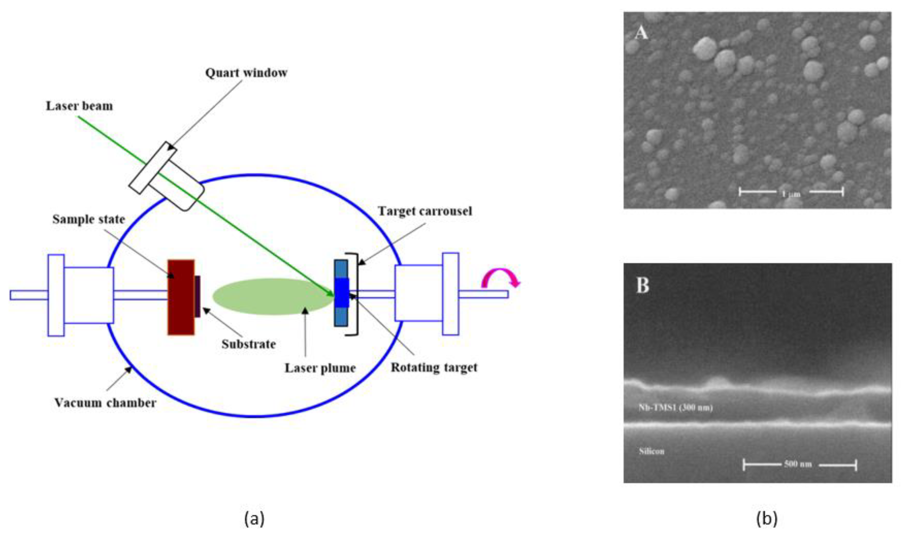
3.4. Pulsed Laser Deposition (PLD)

In the PLD process, in order to prevent disturbance from the ambient atmosphere, the target material together with the substrate are kept in a vacuum chamber, with the directed pulsed laser beam entering the chamber through a fitting opening as illustrated in Figure 10a [108]. Amongst the numerous works conducted with the use of the PLD process, Gimon-Kinsel and Balkus [18], carried out a study on the PLD of mesoporous thin films of NbxOy together with its application on the development of chemical sensors. The as-prepared films underwent SEM as shown in Figure 10b, XRD, and FTIR characterizations, as such the authors stated that the PLD of the mesoporous niobium oxide, Nb-TMS1, and the post-hydrothermal treatment result of the mesoporous thin film had what appeared as a three-dimensional disorganized hexagonal shape, with the cause of the disoriented shape not certain. The thin films of the mesoporous Nb-TMS1 were used as a dielectric phase in the chemical sensors of capacitive-type. They discovered the mesoporous niobium oxide-based sensors to be the sensors with excellent humidity, displaying capacitance transformations of at least 10 times above that of methanol, nitrogen, acetone, and ammonia. Also, it was stated that the Nb-TMS1 reliant sensors exhibited H2O responses that were a thousand times beyond that of the dense Nb2O5 based sensors formed by the PLD process.
In a different study by Kyooho et al. [109] they examined the leakage conduction movement within an amorphous resistive-switching thin film of NbxOy squeezed in-between electrodes of platinum. The films which were grown with the use of the pulsed laser deposition approach, demonstrated unipolar kind of resistance switching properties. The different structural properties of the film were performed using the XRD, RBS, and XPS analysis. The authors explained that the current-voltage features during the initial insulating resistance state (IS) as well as in the bistable high-resistance state (HRS), were formed through the utilization of different leakage conduction mechanisms. They revealed that the electroforming process brought about a variation of the dominant conduction mechanisms within the IS and the HRS. Thermionic emissions were also noticed in both the IS and HRS. However, there was a smaller thermal activation energy noticed in the HRS, and the cause of this was not reported.
High versatility for the deposition of materials with distinct film thicknesses, fast, flexible and inexpensive deposition processes are some of the advantages of the PLD process. So also, irregular material coverages, occurrence of splattering liquid droplets, and loss of evaporative materials are significant disadvantages of the process [110,111,112,113].

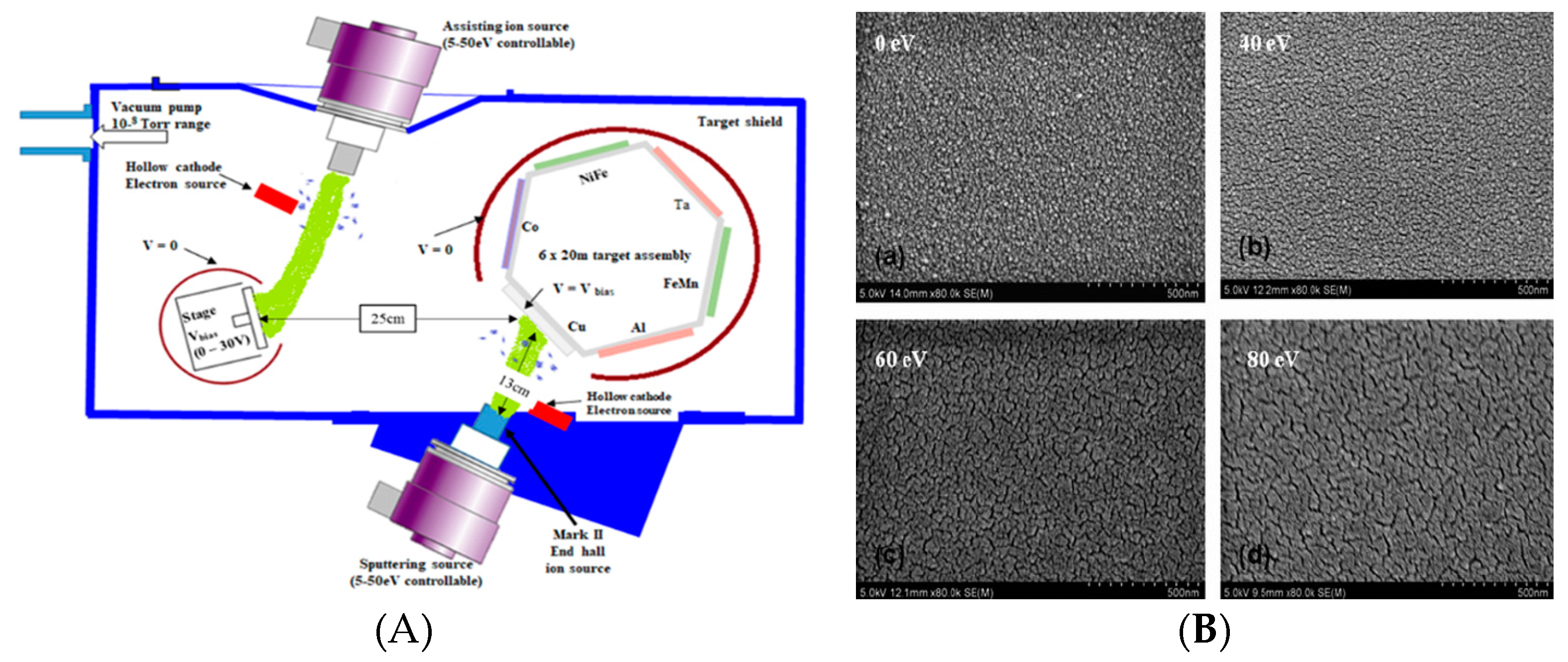
3.5. Biased Target Ion Beam Deposition (BTIBD)

The reactive BTIBD method was established as an improvement for the traditional IBD, with the main advantage of being able to use a low energy ion source which generates inert gas ions of excessively high-density that possess extremely low energy [114] (Figure 11A) [49]. In a bid to acquire more knowledge about the BTIBD method, several studies have been carried out which include the synthesis of epitaxial thin films of NbO2 on the substrate of Al2O3 (0001) by Wang et al. [49]. Using the XRD along with the Raman spectra the authors confirmed the pure deposited NbO2 film to be of tetragonal phase. With the application of the XPS, they discovered a thick layer of approximately 1.3 nm of Nb2O5 at the surface, with the majority of the thin film being NbO2. They also determined the epitaxial relationship pertaining to the NbO2 film with the substrate and calculated an electrical transport measurement at 400 K. Wang and Co. also performed AFM analysis (Figure 11B) on the film and reported the root mean square (rms) surface roughness to be 0.12 nm.
Another study by Kittiwatanaku et al. [114] illustrated the modification of the surface morphology of NbxOy thin films of 10–100 nm. Application of the AFM analysis revealed that the target current (IT) in conjunction with the target bias (VT) were the primary variables, and thus were identified to be essential for the control over the surface morphology and crystallinity of the NbxOy films. Using the XRD, the authors reported that improved growth conditions produced a NbxOy film with 50 nm thickness alongside a 0.4 nm root-mean-square roughness, which was an order of magnitude finer than the Nb films formed via the sputtering deposition process. The vital superconductivity temperature had a close value with the entire Nb (9.3 K) and also had a remarkable homogeneous transformation as reported by the authors. Although, the basis of this impressive transformation was not explained, the standard of the NbxOy film was apparent when an extremely thin layer of proximity (0.75 nm) was present. They disclosed that the outcomes from the experiment showed that the formation of fine NbxOy films with the predicted superconductivity by the BTIBD process could function as base electrode for either in situ magnetic layer or as an insulating layer in superconducting electronic systems.
Apart from being able to use a low energy ion source, the BTIBD deposition process has the advantage of controllability of the ions incident on the growing surface, and produces high quality surfaces as well. It also enables variations of independent ion species as well as current density of the ion beams. However, high complexity level, high cost of maintenance, low deposition rates, and difficulty in scaling up are some of the disadvantages of this process [48,114,115].

3.6. Electron Beam Evaporation (E-beam)

The E-beam evaporation method is a PVD process, which at relatively low substrate temperatures produces a high rate of deposition between 0.1 μm/min and 100 μm/min. The evaporation process occurs in a vacuum, typically at a pressure of 10−5 torr. A current of 5 to 10 kV is passed via a tungsten filament which heats it up to the moment where thermionic emission of the electrons occurs (Figure 12a) [117]. In order to have more understanding of the electron beam evaporation process, Ahmad et al. [118] examined the effect of the preparatory conditions on the optical characteristics of niobium oxide thin films. The authors explained that the primary parameters of deposition, which included the partial pressure of oxygen alongside the temperature of substrate, which were constant during the film deposition process, influenced the optical features of the E-beam evaporated films of niobium oxide. They reported the entire deposited films to be of amorphous structure as shown with the XRD analysis. The authors also reported to have observed considerable variations within the optical constants and the optical energy bandgap after alterations were made to the preparatory conditions of the process. These changes are in relation to the equivalent compositional variations, noticed in the Rutherford backscattering spectroscopy (RBS), during the oxygen to niobium atomic ratio of the films formed under varying conditions.
A different study by Bockute et al. [119] investigated Lanthanum niobium oxide (LaNb7O12) thin films produced via the application of the electron beam physical vapour deposition (EB-PVD) process. The outcomes from the XRD spectra study showed that both La2O3 and NbxOy films possessed distinct rates of deposition, which meant that the stoichiometry of the materials in the produced thin films were different from the original material prior to the evaporation process. The 1 La:1 Nb stoichiometry was attained when the initial oxides molar ratio was 1.3 La2O3:1 NbxOy. This meant that equal reactant of Lanthanum and niobium were attained only when the molar ratio of their initial oxides were in the ratio of 1.3:1. Through the SEM analysis (Figure 12b), Bockute and Co. stated that the prepared thin films all possessed amorphous kind of structures. They also reported that the molar mixing ratio of La2O3 together with NbxOy powders had no effect on the thin films’ crystallinity, however, the reason for the lack of effect was not specified. Bockute and Co. made a discovery on the refractive indexes being contingent on the volume of lanthanum contained in the thin films, with also having the possibility to reduce with a rising lanthanum quantity. They also realized the measured optical band gaps of the films to be between the ranges of 3.69 to 3.9 eV [98]. The E-Beam method of film fabrication has high efficiency in material utilization, extremely high deposition rates and provision for morphological and structural film control as its advantages. While disadvantages of this process include, not being able to coat the internal surfaces of complex geometries, X-ray destruction, difficulty in enhancement of its step coverage [120,121,122].

3.7. Electrochemical Deposition Process (ECD)

The electrochemical deposition process functions based on certain basic electrochemical characteristics [123]. Anode and cathode electrodes are submerged in an electrolytic solution already consisting of liquefied metal salts, in addition to some other ions that allow sufficient current flow as demonstrated in Figure 13A. Lee and Crayston [124] explored different approaches for electrodepositing niobium oxide via aqueous and non-aqueous solutions. The techniques which were applied depended on the pH electrochemical control that resulted in the hydrolysis of soluble, precise niobium precursors, which brought about the deposition of oxides at the electrode. In the non-aqueous solution which comprised of niobium alkoxides, the authors described that hydroxide ions were created using the two-electron reduction of tertiary alcohols at c −2.5 V, which reacted with the niobium precursor, generating a niobium oxide film on the collapsing electrode of mercury. However, they stated that hydroxide formation through the reduction of oxygen to superoxide within the O, -saturated, non-aqueous solvents consisting of NbC1, was not able to produce niobium oxide films, even though the rationale behind this was not explained. During the acidic aqueous solution which contained species of [NbCl5I2], Lee and Crayston described an increase in the local pH close to the electrode, with the development of hydrogen prompting the deposition of niobium oxide away from the electrode. While in the aqueous alkaline solutions of niobates K,H [NbO] or tetramethylammonium [Nb10O28], the protons formed via electrochemical oxidation of water at a value greater than +1.5 V effected the fabrication of combined films of niobate and niobium oxides over the electrode, following an interval of more than 30 min. The different fabricated film’s structure and compositions were characterized with the use of SEM (Figure 13B), XRD, and FTIR.
In a separate study by Cai et al. [125], a synthesis was conducted on niobium(V) ethoxide C10H25NbO5 by making use of the electrochemical reaction of ethanol, with the anode represented as niobium plate, stainless steel utilized as cathode, and tetraethylammonium chloride (TEAC) being the additive for conduction. The sample which underwent characterization via the Fourier transform infrared (FTIR) spectra, the Raman spectra, as well as the nuclear magnetic resonance (NMR) spectra, demonstrated that the sample was niobium ethoxide. The impurity concentrations of the metallic elements within the product were revealed through the ICP-MS, and this showed that purity level of the sample could go as high as 99.997%, as reported by the authors. They further pointed out that volatility, together with purity of the niobium ethoxide assures that it makes an excellent precursor in the CVD and ALD of niobium oxide layers.
The ECD process unlike the chemical spray pyrolysis process has the advantages of scalability, affordability and simplicity as its merits. However, it has the propensity to produce non-conformal growths on irregular surfaces, consumes a lot of time, and is a source of pollution through waste disposal derived from the electroplating process [126,127,128].

3.8. Chemical Vapour Deposition Process (CVD)

The traditional CVD process comprises of a combination of gaseous reactant precursors transported simultaneously to a reactor chamber (Figure 14A). The reactant precursors consequently undergo reaction with the heated substrate material resulting in thin solid films on the surface of the substrate. One of the multiple studies using the CVD technique was conducted by Bharti and Rhee [36] on the growth of thin films of niobium oxide through absolute liquid injection CVD with the use of Nb(C2H5)5 as precursor. Interpreting the XDR analysis, the authors reported that the films were only noticed to begin crystallization at a temperature higher than 340 °C in the O2 atmosphere, and became crystalline at a temperature of 400 °C. The crystalline films possessed a surface texture that was greatly influenced by the temperature of deposition and the reactant’s molar ratios. They stated that a reduction in the surface coarseness enhanced the leakage current. However, the relationship between the film’s surface coarseness and the leakage current was not stated. The XPS analysis revealed the films to be in distinct states of oxidation (Nb2+, Nb4+ and Nb5+). It was also observed by the authors that the dielectric constants of the films were increased via an increment in the oxygen ratios. They reported that at a ratio of 150:1, the film exhibited high dielectric constant of 47 when at a temperature of 340 °C and a 2.0 × 10⁻⁵ A/cm2 leakage current density at 3 V.
A similar study by Fiz et al. [130] reported on the characterization, the electrochemical characteristics, and the controlled synthesis of various NbxOy polymorphs grown through the CVD of novel single-source precursors. The films of NbxOy prepared at varying temperatures revealed the SEM (Figure 14B), and XRD analysis systematic phase transformation from a low temperature tetragonal (TT-Nb2O5, T-Nb2O5) to a high temperature monoclinic modification (H−Nb2O5). Also, with respect to the AFM analysis, the authors noted an improvement in the precursor flux and substrate temperature which permitted phase-selective growths of NbxOy films and nanorods on the conductive mesoporous biomorphic carbon matrices (BioC). The thin films of Nb2O5, which were prepared on the monolithic BioC scaffolds resulted in composite materials that integrated with the nanostructured niobium oxide’s high capacitance. Heterojunctions within the composites of Nb2O5/BioC were discovered to be of importance in the electrochemical capacitance, though their level of importance was not defined. From the XPS study, the authors stated that the electrochemical analysis of the composites of Nb2O5/BioC revealed that little quantities of Nb2O5 (as low as 5%) and BioCarbon had caused an increase of 7-folds in the electrode capacitance, while transmitting excellent cycling stability, and getting the materials perfectly appropriate for electrochemical energy storage applications.
The CVD process possesses the advantages of; the derived films being fairly conformal, enables high deposition rates of material, and allows concurrent introduction of materials. Some of its disadvantages includes, inappropriate for extremely thin films, lacks conformity on substrate surfaces of very high aspect ratios, uses high deposition temperatures [131,132,133,134].

3.9. Atomic Layer Deposition (ALD)

As demonstrated in Figure 15A, the ALD cycle generally constitutes a cycle of four steps, performed based on the number of times required in order to attain the needed deposition film thickness, and these four steps are dependent on time measured in seconds. The ALD process is a crucial method for the manufacture of semiconductor products and it is also among the tools set available for nanomaterial synthesis. For the purpose of acquiring more knowledge on the ALD processes, several studies have been conducted with the use of the process which include, the resistive switching behaviour of NbxOy analysed as favourite for subsequent generation of non-volatile memory technology by Chen et al. [135]. At 300 °C, the authors stated that the crystalline form of the films deposited was detected to be of polycrystalline form with the use of the XRD analysis, although the film structure below 300 °C was not revealed. Also, a calculation carried out on the film through the application of the XPS studies, discovered the film to have a deficiency in oxygen. Chen and Co. explained that the low resistance “ON” state (LRS), together with the high resistance “OFF” state (HRS), were altered reversibly with a minimal voltage of around ±1 V for the reaction process. They reported that over a thousand reproducible switching cycles performed by the DC voltage sweep could be noticed to have resistance ratios beyond 10, this was quite significant for memory applications. They further revealed that the HRS along with the LRS of the components were steady for over 5 × 10⁴ s, thus showed no sign of any degradation whatsoever during the test.
Another study by Huang et al. [61] investigated ultra-thin films of Nb2O5 with good uniformity being deposited on Si (100) with the use of Nb (C2H5)5 in conjunction with H2O as precursor species. The results from the AFM study indicated ultra-thin films of Nb2O5 (approximately 3 nm) being slowly formed into scattered large islands which have rising rapid thermal annealing (RTA) temperature. They disclosed that the crystalline phase and amorphous phase of the film were created in the Nb2O5 matrix which underwent the process of annealing at 700 °C. With regards to the as-deposited film, the authors identified through the AFM, an interfacial layer (IL) possessing an approximately 1.5 nm thickness, consisting of niobium silicate (Nb–O–Si), nevertheless, the reason of this thickness was unexplained. Additionally, the high-temperature RTA generated a thickened IL, that was in relation to the production of additional Nb–O–Si bonds along with fresh silicon oxide (Si–O–Si) next to the Si (100).
Nivedita et al. (2020) in one of his studies, fabricated a NbO thin film through the ALD process and characterized the films with SEM micrographs at varying substrate temperatures of 25–700 °C as shown in Figure 15B. They reported that there was a resulting decrease in the Nb films thickness when the deposition temperature was increased. The advantages of the process include its ability to produce precise film thicknesses, its reproducibility, and ease of control. The process also efficiently creates ultra-uniform thin films on surfaces of extremely high-aspect-ratios and allows batch depositions since it permits reactions only at the interface. Lengthy deposition rates, very high cost of equipment as well as nanoparticles emission during the course of the reaction are major disadvantages of the process [136,137,138,139].
Furthermore, apart from the sol-gel process being an inexpensive one, the sol-gel process unlike the most other preparation methods has extensive doping characteristics, this is due to the doping procedure being able to be controlled. However, there is the challenge of avoidance of residual porosity and OH groups [141], in contrast to other deposition techniques. Thus, the niobium oxide thin film produced via the sol-gel process are well suited for sensing and electrochromic properties in contrast to other fabrication methods. Similarly, notwithstanding the advantages of spherical morphology and compositional homogeneity, the chemical spray pyrolysis method possesses over other deposition processes, it also has the benefit of the film’s composition being controllable [142]. Nevertheless, this system of fabrication possesses the difficulty of ascertaining the actual temperature of the film growth. Catalytic applications as well as proton exchange membrane applications have more significance in niobium oxide spray pyrolysis manufactured films than other deposition techniques.
The sputtering process unlike many other manufacturing approaches has the vital benefit of materials having extremely high melting points being able to be sputtered comfortably (Table 2). Nonetheless, the process acquires the demerit of a non-uniform deposition flow distribution. Niobium oxide films produced via the sputter deposition are very suitable for semi-conductor materials, architectural coatings and computer hard disk [104], in contrast to other preparation processes.
The pulsed laser deposition technique disparate from most deposition techniques possesses the unique advantage of its source of energy being outside of the vacuum chamber, also, the process allows most condensed material matter to be subjected to ablation. However, unlike other deposition approaches, it possesses the disadvantage of some of its plume species initiating re-sputtering and subsequent defects on the surface of the substrate and the developing film due to high kinetic energy [143]. Diamond-like coatings and superconducting devices have usefulness in niobium oxide pulsed lased deposition thin films than other production methods.
The biased target ion beam deposition technique in comparison to other deposition procedures is distinguished by its reduced process pressure, its exclusive target control and its superior surface quality [115]. Nevertheless, the process has the demerits of low rates of deposition, high complexity level compared to most film formation processes. Niobium oxide thin films produced from biased ion beam deposition process have more importance in electronic devices, reflective mirrors and RF neutralizers (Table 2).
Besides the ability of the electron beam evaporation process to heat materials to increased temperatures, there is also the benefit of high film deposition rates when compared to fabrication approaches. Irrespective of that, there is the challenge of controlling the film composition in contrast to other preparation methods, like the sputtering process. The niobium oxide thin films obtained from the e-beam process are very suitable for thermoelectric materials coatings, solar applications, thermal barrier coatings contrary to other methods of deposition [121].
The electrochemical deposition process unlike most deposition techniques has the benefit of an enhanced interfacial bonding involving the material to be coated and the substrate prior to the application of heat. Though, it possesses the downside of producing non-conformal growths on uneven surfaces while using this technique [144]. Decorative coatings, energy storages, and separation techniques are appropriate for niobium oxide thin films produced from the electrochemical deposition process as against other techniques used for film production.
The CVD process in variation to other manufacturing processes, uniquely has the merits of concurrent materials introduction, and source materials flowing through the outside reservoirs which can be replenished without contaminating the growth region [145]. However, the plasma CVD process encounters difficulties in film stoichiometry control as a result of differences in the bond strengths of varying precursors. Dielectrics, conductors, and fiber composites all have suitability in CVD thin films of niobium oxide in contrast to other process of deposition. Notwithstanding, the ALD process which arguably is the best deposition process ideally distinguishing itself from other deposition procedures, possesses the advantages of producing ultra-thin films, high density of film, outstanding film reproducibility, and pin-hole free films amongst many others [146]. However, the process like every other deposition method has its demerits which include; high material and energy wastage, nanoparticle emissions, extended deposition time [147]. The niobium oxide thin films produced from the ALD process are well suited for microelectronics, fuel cells, Li-ion batteries, transistors, conformal and nano-coatings, microelectromechanical systems (MEMS) in comparison to the other fabrication processes.

4. Conclusions

With the use of distinct preparation techniques, thin films of NbO, NbO2 and Nb2O5 were appropriately produced. The fabricated thin films experienced analysis and, characterization with the application of varying distinct processes such as, NIR, ICP-MS, XRD, FTIR, XPS, NMR and UV-Visible spectrophotometer. From this study, the characteristics of the manufactured NbxOy thin films such as film thickness, surface quality, interface properties, and optical properties are all in relation to the distinct deposition processes implemented. NbxOy film’s outstanding quality has gained substantial interest in academia, and its fabrication methods have interestingly already obtained some research results. Their production technique is predicted to even develop more, and the NbxOy film with even more sustained performance can progressively attain more industrialization with broader application areas being created.

Supplementary Materials

The following are available online at https://www.mdpi.com/2079-6412/10/12/1246/s1, Figure S1: XPS spectra showing the empty substrate together with the Niobium-coated steel. The binding energy of the Niobium peaks was visible at: Nb 3d3/2 (202 eV), Nb 3d5/2 (205 eV), Nb 3p3/2 (360.6 eV) and Nb 3p1/2 (376.5 eV).

Author Contributions

N.C.E., contributed towards conceptualization and writing of the original draft of the article. P.E.I. contributed in the aspect of reviewing, validating and editing of the article and T.-C.J. also contributed in the area of conceptualization, resources, reviewing and editing, and supervision. All authors have read and agreed to the published version of the manuscript.

Funding

This research received no external funding and The APC was funded by University of Johannesburg, South Africa.

Acknowledgments

The authors hereby devote acknowledgement to the University Research Commission (URC), the Global Excellence Stature (GES) as well as the National Research Foundation (NRF) South Africa for being supportive financially.

Conflicts of Interest

The authors declare no conflict of interest. Also, the funders had no role in the design of the study; in the collection, analyses, or interpretation of data; in the writing of the manuscript, or in the decision to publish the results.

References

  1. Meija, J.; Coplen, T.B.; Berglund, M.; Brand, W.A.; De Bièvre, P.; Gröning, M.; Holden, N.E.; Irrgeher, J.; Loss, R.D.; Walczyk, T.; et al. Atomic weights of the elements 2013 (IUPAC Technical Report). Pure Appl. Chem. 2016, 88, 265–291. [Google Scholar] [CrossRef]
  2. Samsonov, G.V. Mechanical Properties of the Elements. In Handbook of the Physicochemical Properties of the Elements; Springer Science and Business Media: Berlin/Heidelberg, Germany, 1968; pp. 387–446. [Google Scholar]
  3. Knapp, B. Elements of Geographical Hydrology; Unwin Hyman Limited: London, UK, 2002. [Google Scholar]
  4. Zhao, Y.; Zhang, Z.; Lin, Y. Optical and dielectric properties of a nanostructured NbO2 thin film prepared by thermal oxidation. J. Phys. D: Appl. Phys. 2004, 37, 3392–3395. [Google Scholar] [CrossRef]
  5. Tanabe, K. Catalytic application of niobium compounds. Catal. Today 2003, 78, 65–77. [Google Scholar] [CrossRef]
  6. Jacob, K.T.; Shekhar, C.; Vinay, M.; Waseda, Y. Thermodynamic Properties of Niobium Oxides. J. Chem. Eng. Data 2010, 55, 4854–4863. [Google Scholar] [CrossRef]
  7. Venkataraj, S.; Drese, R.; Liesch, C.; Kappertz, O.; Jayavel, R.; Wuttig, M. Temperature stability of sputtered niobium–oxide films. J. Appl. Phys. 2002, 91, 4863–4871. [Google Scholar] [CrossRef]
  8. Bach, D.; Stormer, H.; Schneider, R.; Gerthsen, D.; Sigle, W. EELS Investigations of Reference Niobium Oxides and Anodically Grown Niobium Oxide Layers. Microsc. Microanal. 2007, 13. [Google Scholar] [CrossRef]
  9. Foroughi-Abari, A.; Cadien, K.C. Growth, structure and properties of sputtered niobium oxide thin films. Thin Solid Films 2011, 519, 3068–3073. [Google Scholar] [CrossRef]
  10. Venkataraj, S.; Drese, R.; Kappertz, O.; Jayavel, R.; Wuttig, M. Characterization of Niobium Oxide Films Prepared by Reactive DC Magnetron Sputtering. Phys. Status Solidi 2001, 188, 1047–1058. [Google Scholar] [CrossRef]
  11. Ou, J.Z.; Rani, R.A.; Ham, M.-H.; Field, M.R.; Zhang, Y.; Zheng, H.; Reece, P.; Zhuiykov, S.; Sriram, S.; Bhaskaran, M.; et al. Elevated Temperature Anodized Nb2O5: A Photoanode Material with Exceptionally Large Photoconversion Efficiencies. ACS Nano 2012, 6, 4045–4053. [Google Scholar] [CrossRef]
  12. Reichman, B.; Bard, A.J. Electrochromism at Niobium Pentoxide Electrodes in Aqueous and Acetonitrile Solutions. J. Electrochem. Soc. 1980, 127, 241–242. [Google Scholar] [CrossRef] [Green Version]
  13. Granqvist, C. Inorganic Non-Oxide Electrochromic Materials. In Handbook of Inorganic Electrochromic Materials; Elsevier: Amsterdam, The Netherlands, 1995; pp. 421–430. [Google Scholar]
  14. Cabanel, R.; Chaussy, J.; Mazuer, J.; Delabouglise, G.; Joubert, J.C.; Barral, G.; Montella, C. Electrochemichromism of Nb2O5 Thin Films Obtained by Oxidation of Magnetron-Sputtered NbNx. J. Electrochem. Soc. 1990, 137, 1444–1451. [Google Scholar] [CrossRef]
  15. Schmitt, M.; Aegerter, M. Electrochromic properties of pure and doped Nb2O5 coatings and devices. Electrochimica Acta 2001, 46, 2105–2111. [Google Scholar] [CrossRef] [Green Version]
  16. Mujawar, S.; Inamdar, A.; Patil, P.; Patil, P. Electrochromic properties of spray-deposited niobium oxide thin films. Solid State Ionics 2006, 177, 3333–3338. [Google Scholar] [CrossRef]
  17. Granqvist, C. Electrochromism and smart window design. Solid State Ionics 1992, 53, 479–489. [Google Scholar] [CrossRef]
  18. E Gimon-Kinsel, M.; Balkus, J.K.J. Pulsed laser deposition of mesoporous niobium oxide thin films and application as chemical sensors. Microporous Mesoporous Mater. 1999, 28, 113–123. [Google Scholar] [CrossRef]
  19. Rho, S.; Jahng, D.; Lim, J.H.; Choi, J.; Chang, J.H.; Lee, S.C.; Kim, K.J. Electrochemical DNA biosensors based on thin gold films sputtered on capacitive nanoporous niobium oxide. Biosens. Bioelectron. 2008, 23, 852–856. [Google Scholar] [CrossRef]
  20. Ficarro, S.B.; Parikh, J.R.; Blank, N.C.; Marto, J.A. Niobium(V) Oxide (Nb2O5): Application to Phosphoproteomics. Anal. Chem. 2008, 80, 4606–4613. [Google Scholar] [CrossRef]
  21. Tamai, T.; Haneda, M.; Fujitani, T.; Hamada, H. Promotive effect of Nb2O5 on the catalytic activity of Ir/SiO2 for NO reduction with CO under oxygen-rich conditions. Catal. Commun. 2007, 8, 885–888. [Google Scholar] [CrossRef]
  22. Cvelbar, U.; Mozetič, M. Behaviour of oxygen atoms near the surface of nanostructured Nb2O5. J. Phys. D: Appl. Phys. 2007, 40, 2300–2303. [Google Scholar] [CrossRef]
  23. Prado, A.G.; Bolzon, L.B.; Pedroso, C.P.; Moura, A.O.; Costa, L.L. Nb2O5 as efficient and recyclable photocatalyst for indigo carmine degradation. Appl. Catal. B Environ. 2008, 82, 219–224. [Google Scholar] [CrossRef]
  24. Eisenbarth, E.; Velten, D.; Breme, J. Biomimetic implant coatings. Biomol. Eng. 2007, 24, 27–32. [Google Scholar] [CrossRef] [PubMed]
  25. Starikov, V.V.; Starikova, S.L.; Mamalis, A.G.; Lavrynenko, S.N.; Ramsden, J.J. The application of niobium and tantalum oxides for implant surface passivation. J. Biol. Phys. Chem. 2007, 7, 65–68. [Google Scholar] [CrossRef]
  26. Tanvir, M.T.; Aoki, Y.; Habazaki, H. Improved electrical properties of silicon-incorporated anodic niobium oxide formed on porous Nb–Si substrate. Appl. Surf. Sci. 2009, 255, 8383–8389. [Google Scholar] [CrossRef]
  27. Le Viet, A.; Reddy, M.V.; Jose, R.; Chowdari, B.V.R.; Ramakrishna, S. Nanostructured Nb2O5 Polymorphs by Electrospinning for Rechargeable Lithium Batteries. J. Phys. Chem. C 2010, 114, 664–671. [Google Scholar] [CrossRef]
  28. Blanquart, T.; Niinistö, J.; Heikkilä, M.; Sajavaara, T.; Kukli, K.; Puukilainen, E.; Xu, C.; Hunks, W.; Ritala, M.; Leskelä, M. Evaluation and Comparison of Novel Precursors for Atomic Layer Deposition of Nb2O5 Thin Films. Chem. Mater. 2012, 24, 975–980. [Google Scholar] [CrossRef]
  29. Zhou, X.; Li, Z.; Wang, Y.; Sheng, X.; Zhang, Z. Photoluminescence of amorphous niobium oxide films synthesized by solid-state reaction. Thin Solid Films 2008, 516, 4213–4216. [Google Scholar] [CrossRef]
  30. Lai, F.; Lin, L.; Huang, Z.; Gai, R.; Qu, Y. Effect of thickness on the structure, morphology and optical properties of sputter deposited Nb2O5 films. Appl. Surf. Sci. 2006, 253, 1801–1805. [Google Scholar] [CrossRef]
  31. Störmer, H.; Weber, A.; Fischer, V.; Ivers-Tiffée, E.; Gerthsen, D. Anodically formed oxide films on niobium: Microstructural and electrical properties. J. Eur. Ceram. Soc. 2009, 29, 1743–1753. [Google Scholar] [CrossRef]
  32. Yoon, J.S.; Cho, S.W.; Kim, Y.S.; Kim, B.I. The production of niobium powder and electric properties of niobium capacitors. Met. Mater. Int. 2009, 15, 405–408. [Google Scholar] [CrossRef]
  33. Choi, J.; Lim, J.H.; Lee, J.; Kim, K.J. Porous niobium oxide films prepared by anodization–annealing–anodization. Nanotechnology 2007, 18, 055603. [Google Scholar] [CrossRef]
  34. Matylitskaya, V.A.; Bock, W.; Kolbesen, B.O. Nitridation of niobium oxide films by rapid thermal processing. Anal. Bioanal. Chem. 2008, 390, 1507–1515. [Google Scholar] [CrossRef] [PubMed]
  35. Kukli, K.; Ritala, M.; Leskelä, M. Development of Dielectric Properties of Niobium Oxide, Tantalum Oxide, and Aluminum Oxide Based Nanolayered Materials. J. Electrochem. Soc. 2001, 148, F35–F41. [Google Scholar] [CrossRef]
  36. Bharti, D.C.; Rhee, S.-W. Dielectric properties and X-ray photoelectron spectroscopic studies of niobium oxide thin films prepared by direct liquid injection chemical vapor deposition method. Thin Solid Films 2013, 548, 195–201. [Google Scholar] [CrossRef]
  37. Cho, K.; Lee, J.; Lim, J.-S.; Lim, H.; Lee, J.; Park, S.; Yoo, C.-Y.; Kim, S.-T.; Chung, U.-I.; Moon, J.-T. Low temperature crystallized Ta2O5/Nb2O5 bi-layers integrated into RIR capacitor for 60 nm generation and beyond. Microelectron. Eng. 2005, 80, 317–320. [Google Scholar] [CrossRef]
  38. Naito, K.; Matsui, T. Review on phase equilibria and defect structures in the niobium-oxygen system. Solid State Ionics 1984, 12, 125–134. [Google Scholar] [CrossRef]
  39. Augustyn, V.; Come, J.; Lowe, M.A.; Kim, J.W.; Taberna, P.-L.; Tolbert, S.H.; Abruña, H.D.; Simon, P.; Dunn, B. High-rate electrochemical energy storage through Li+ intercalation pseudocapacitance. Nat. Mater. 2013, 12, 518–522. [Google Scholar] [CrossRef]
  40. Tamang, R.; Varghese, B.; Mhaisalkar, S.; Tok, E.S.; Sow, C.H. Probing the photoresponse of individual Nb2O5 nanowires with global and localized laser beam irradiation. Nanotechnol. 2011, 22, 115202. [Google Scholar] [CrossRef]
  41. Hulm, J.K.; Jones, C.K.; Hein, R.A.; Gibson, J.W. Superconductivity in the TiO and NbO systems. J. Low Temp. Phys. 1972, 7, 291–307. [Google Scholar] [CrossRef]
  42. Lo, W.; A Cardwell, D.; Bradley, A.D.; Doyle, R.; Shi, Y.; Lloyd, S. Development of non-weak link bulk YBCO grain boundaries for high magnetic field engineering applications. IEEE Trans. Appl. Supercond. 1999, 9, 2042–2045. [Google Scholar] [CrossRef]
  43. Shin, S.H.; Halpern, T.; Raccah, P.M. High-speed high-current field switching of NbO2. J. Appl. Phys. 1977, 48, 3150. [Google Scholar] [CrossRef]
  44. Sasaki, K.; Adzic, R.R. Monolayer-level Ru-and NbO2-supported platinum electrocatalysts for methanol oxidation. J. Electrochem. Soc. 2008, 155, B180–B186. [Google Scholar] [CrossRef]
  45. Bolzan, A.A.; Fong, C.; Kennedy, B.J.; Howard, C.J. A Powder Neutron Diffraction Study of Semiconducting and Metallic Niobium Dioxide. J. Solid State Chem. 1994, 113, 9–14. [Google Scholar] [CrossRef]
  46. Eyert, V. The metal-insulator transition of NbO2: An embedded Peierls instability. EPL Europhysics Lett. 2002, 58, 851–856. [Google Scholar] [CrossRef] [Green Version]
  47. Kim, S.; Park, J.; Woo, J.; Cho, C.; Lee, W.; Shin, J.; Choi, G.; Park, S.; Lee, D.; Lee, B.H.; et al. Threshold-switching characteristics of a nanothin-NbO2-layer-based Pt/NbO2/Pt stack for use in cross-point-type resistive memories. Microelectron. Eng. 2013, 107, 33–36. [Google Scholar] [CrossRef]
  48. Pickett, M.D.; Williams, R.S. Sub-100 fJ and sub-nanosecond thermally driven threshold switching in niobium oxide crosspoint nanodevices. Nanotechnol 2012, 23, 215202. [Google Scholar] [CrossRef] [PubMed]
  49. Wang, Y.; Comes, R.B.; Kittiwatanakul, S.; Wolf, S.A.; Lu, J. Epitaxial niobium dioxide thin films by reactive-biased target ion beam deposition. J. Vac. Sci. Technol. A 2015, 33, 21516. [Google Scholar] [CrossRef]
  50. Lee, S.-H.; Yoon, H.-N.; Yoon, I.; Kim, B.-S. Single Crystalline NbO2 Nanowire Synthesis by Chemical Vapor Transport Method. Bull. Korean Chem. Soc. 2012, 33, 839–842. [Google Scholar] [CrossRef] [Green Version]
  51. Ramírez, G.; Rodil, S.; Muhl, S.; Turcio-Ortega, D.; Olaya, J.; Rivera, M.; Camps, E.; Escobar-Alarcón, L. Amorphous niobium oxide thin films. J. Non-Crystalline Solids 2010, 356, 2714–2721. [Google Scholar] [CrossRef]
  52. Kato, K. Structure refinement of H-Nb2O5. Acta Crystallogr. Sect. B Struct. Crystallogr. Cryst. Chem. 1976, 32, 764–767. [Google Scholar] [CrossRef]
  53. Kato, K.; Tamura, S. Die Kristallstruktur von T-Nb2O5. Acta Crystallogr. Sect. B Struct. Crystallogr. Cryst. Chem. 1975, 31, 673–677. [Google Scholar] [CrossRef]
  54. Holser, W.T. Compounds with the α-U3O8-type structure. Acta Crystallogr. 1956, 9, 196. [Google Scholar] [CrossRef] [Green Version]
  55. Ikeya, T.; Senna, M. Change in the structure of niobium pentoxide due to mechanical and thermal treatments. J. Non-Crystalline Solids 1988, 105, 243–250. [Google Scholar] [CrossRef]
  56. Cho, N.-H.; Kang, H.B.; Kim, Y.H. Dielectric characteristics and chemical structures of Nb2O5 thin films grown by sol-gel techniques. Ferroelectrics 1994, 152, 43–48. [Google Scholar] [CrossRef]
  57. Kumagai, N.; Tanno, K.; Nakajima, T.; Watanabe, N. Structural changes of Nb2O5 and V2O5 as rechargeable cathodes for lithium battery. Electrochimica Acta 1983, 28, 17–22. [Google Scholar] [CrossRef]
  58. Maček, M.; Orel, B. Electrochromism of sol–gel derived niobium oxide films. Sol. Energy Mater. Sol. Cells 1998, 54, 121–130. [Google Scholar] [CrossRef] [Green Version]
  59. Jelle, B.P. Electrochromic Smart Windows for Dynamic Daylightand Solar Energy Control in Buildings. Electrochromic Mater. Devices 2015, 419–502. [Google Scholar] [CrossRef]
  60. Zhitomirsky, I. Electrolytic deposition of niobium oxide films. Mater. Lett. 1998, 35, 188–193. [Google Scholar] [CrossRef]
  61. Huang, Y.; Xu, Y.; Ding, S.-J.; Lu, H.-L.; Sun, Q.-Q.; Zhang, D.W.; Chen, Z. Thermal stability of atomic-layer-deposited ultra-thin niobium oxide film on Si (100). Appl. Surf. Sci. 2011, 257, 7305–7309. [Google Scholar] [CrossRef]
  62. Nowak, I.; Ziolek, M. Niobium Compounds: Preparation, Characterization, and Application in Heterogeneous Catalysis. Chem. Rev. 1999, 99, 3603–3624. [Google Scholar] [CrossRef]
  63. Rani, R.A.; Zoolfakar, A.S.; O’Mullane, A.P.; Austin, M.W.; Kalantar-Zadeh, K. Thin films and nanostructures of niobium pentoxide: fundamental properties, synthesis methods and applications. J. Mater. Chem. A 2014, 2, 15683–15703. [Google Scholar] [CrossRef] [Green Version]
  64. Le Viet, A.; Jose, R.; Reddy, M.V.; Chowdari, B.V.R.; Ramakrishna, S. Nb2O5 Photoelectrodes for Dye-Sensitized Solar Cells: Choice of the Polymorph. J. Phys. Chem. C 2010, 114, 21795–21800. [Google Scholar] [CrossRef]
  65. Reznichenko, L.A.; Akhnazarova, V.V.; Shilkina, L.A.; Razumovskaya, O.N.; Dudkina, S.I. Invar effect in n-Nb2O5, α ht-Nb2O5, and L-Nb2O5. Crystallogra. Rep. 2009, 54, 483–491. [Google Scholar] [CrossRef]
  66. Schäfer, H.; Gruehn, R.; Schulte, F. The Modifications of Niobium Pentoxide. Angew. Chem. Int. Ed. 2003, 5, 40–52. [Google Scholar] [CrossRef]
  67. Ko, E.; Weissman, J. Structures of niobium pentoxide and their implications on chemical behavior. Catal. Today 1990, 8, 27–36. [Google Scholar] [CrossRef]
  68. Lubimtsev, A.A.; Kent, P.R.C.; Sumpter, B.G.; Ganesh, P. Understanding the origin of high-rate intercalation pseudocapacitance in Nb2O5 crystals. J. Mater. Chem. A 2013, 1, 14951–14956. [Google Scholar] [CrossRef]
  69. Wang, Z.; Hu, Y.; Wang, W.; Zhang, X.; Wang, B.; Tian, H.; Wang, Y.; Guan, J.; Gu, H. Fast and highly-sensitive hydrogen sensing of Nb2O5 nanowires at room temperature. Int. J. Hydrogen Energy 2012, 37, 4526–4532. [Google Scholar] [CrossRef]
  70. Palatnikov, M.N.; Shcherbina, O.B.; Sidorov, N.; Skab, I.; Bormanis, K. The structure of niobium and tantalum oxides processed by concentrated light flux. Ukr. J. Phys. Opt. 2012, 13, 207. [Google Scholar] [CrossRef]
  71. Frevel, L.K.; Rinn, H.W. Powder Diffraction Standards for Niobium Pentoxide and Tantalum Pentoxide. Anal. Chem. 1955, 27, 1329–1330. [Google Scholar] [CrossRef]
  72. Norin, R.; Magneli, A. New Niobium Oxide Phases. Naturwissenschaften 1960, 47, 354–355. [Google Scholar] [CrossRef]
  73. Gatehouse, B.M.; Wadsley, A.D. The crystal structure of the high temperature form of niobium pentoxide. Acta Crystallogr. 2002, 17, 1545–1554. [Google Scholar] [CrossRef]
  74. Kubaschewski, O.; Hopkins, B. Oxidation mechanisms of niobium, tantalum, molybdenum and tungsten. J. Less Common Met. 1960, 2, 172–180. [Google Scholar] [CrossRef]
  75. Yan, L.; Rui, X.; Chen, G.; Xu, W.; Zou, G.; Luo, H. Recent advances in nanostructured Nb-based oxides for electrochemical energy storage. Nanoscale 2016, 8, 8443–8465. [Google Scholar] [CrossRef] [PubMed]
  76. Luo, H.; Song, W.; Hoertz, P.G.; Hanson, K.; Ghosh, R.; Rangan, S.; Brennaman, M.K.; Concepcion, J.J.; Binstead, R.A.; Bartynski, R.A.; et al. A Sensitized Nb2O5 Photoanode for Hydrogen Production in a Dye-Sensitized Photoelectrosynthesis Cell. Chem. Mater. 2012, 25, 122–131. [Google Scholar] [CrossRef]
  77. Schultze, J.; Lohrengel, M. Stability, reactivity and breakdown of passive films. Problems of recent and future research. Electrochimica Acta 2000, 45, 2499–2513. [Google Scholar] [CrossRef]
  78. Yoffe, A.D. Low-dimensional systems: Quantum size effects and electronic properties of semiconductor microcrystallites (zero-dimensional systems) and some quasi-two-dimensional systems. Adv. Phys. 2010, 51, 799–890. [Google Scholar] [CrossRef]
  79. Sattler, K. The energy gap of clusters, nanoparticles, and quantum dots. In Handbook of Thin Films; Elsevier: Amsterdam, The Netherlands, 2002; pp. 61–97. [Google Scholar]
  80. Liu, J.; Xue, D.; Li, K. Single-crystalline nanoporous Nb2O5 nanotubes. Nanoscale Res. Lett. 2011, 6, 138. [Google Scholar] [CrossRef] [PubMed] [Green Version]
  81. Greener, E.H.; Whitmore, D.H.; Fine, M.E. Electrical Conductivity of Near-Stoichiometric α-Nb2O5. J. Chem. Phys. 1961, 34, 1017. [Google Scholar] [CrossRef]
  82. Lee, C.-C.; Tien, C.-L.; Hsu, J.-C. Internal stress and optical properties of Nb2O5 thin films deposited by ion-beam sputtering. Appl. Opt. 2002, 41, 2043–2047. [Google Scholar] [CrossRef]
  83. Özer, N.; Rubin, M.D.; Lampert, C.M. Optical and electrochemical characteristics of niobium oxide films prepared by sol-gel process and magnetron sputtering A comparison. Sol. Energy Mater. Sol. Cells 1996, 40, 285–296. [Google Scholar] [CrossRef]
  84. Aegerter, M.A.; Schmitt, M.; Guo, Y. Sol-gel niobium pentoxide coatings: Applications to photovoltaic energy conversion and electrochromism. Int. J. Photoenergy 2002, 4, 1–10. [Google Scholar] [CrossRef] [Green Version]
  85. Pawlicka, A.; Atik, M.; Aegerter, M. Synthesis of multicolor Nb2O5 coatings for electrochromic devices. Thin Solid Films 1997, 301, 236–241. [Google Scholar] [CrossRef] [Green Version]
  86. Xiao, X.; Dong, G.; Xu, C.; He, H.; Qi, H.; Fan, Z.; Shao, J. Structure and optical properties of Nb2O5 sculptured thin films by glancing angle deposition. Appl. Surf. Sci. 2008, 255, 2192–2195. [Google Scholar] [CrossRef]
  87. Çetinörgü-Goldenberg, E.; Klemberg-Sapieha, J.-E.; Martinu, L. Effect of postdeposition annealing on the structure, composition, and the mechanical and optical characteristics of niobium and tantalum oxide films. Appl. Opt. 2012, 51, 6498–6507. [Google Scholar] [CrossRef] [PubMed]
  88. Matias, C.R.; Nassar, E.J.; Verelst, M.; Rocha, L.A. Synthesis and Characterization of Nb2O5:La3+, Eu3+ Phosphors Obtained by the Non-Hydrolytic Sol-Gel Process. J. Braz. Chem. Soc. 2015, 26, 2558–2570. [Google Scholar] [CrossRef]
  89. Sajiki, G.; Benino, Y.; Nanba, T.; Okano, H. Electrochemical and Photoelectrochemical Properties of Nano-Islands of Zinc and Niobium Oxides Deposited on Aluminum Thin Film by RF Magnetron Reactive Sputtering. Mater. Sci. Appl. 2015, 6, 292–309. [Google Scholar] [CrossRef] [Green Version]
  90. Shao, Y.; Yi, K.; Fang, M.; Zhang, J. Properties of niobium oxide films deposited by pulsed DC reactive magnetron sputtering. In Pacific Rim Laser Damage Symposium: Optical Materials for High Power Lasers; SPIE (Society of Photo-Optical Instrumentation Engineers): Bellingham, WA, USA, 2011; Volume 8206, p. 82060M. [Google Scholar]
  91. Shcherbina, O.B.; Palatnikov, M.N.; Efremov, V.V. Mechanical properties of Nb2O5 and Ta2O5 prepared by different procedures. Inorg. Mater. 2012, 48, 433–438. [Google Scholar] [CrossRef]
  92. Özer, N.; Barreto, T.; Büyüklimanli, T.; Lampert, C.M. Characterization of sol-gel deposited niobium pentoxide films for electrochromic devices. Sol. Energy Mater. Sol. Cells 1995, 36, 433–443. [Google Scholar] [CrossRef]
  93. Pierre, A.C. Introduction to Sol-Gel Processing; Springer International Publishing: Cham, Switzerland, 2020; pp. 597–685. [Google Scholar]
  94. Mazdiyasni, K. Powder synthesis from metal-organic precursors. Ceram. Int. 1982, 8, 42–56. [Google Scholar] [CrossRef]
  95. Hanaor, D.A.H.; Chironi, I.; Karatchevtseva, I.; Triani, G.; Sorrell, C.C. Single and mixed phase TiO2powders prepared by excess hydrolysis of titanium alkoxide. Adv. Appl. Ceram. 2012, 111, 149–158. [Google Scholar] [CrossRef] [Green Version]
  96. Thiagarajan, S.; Sanmugam, A.; Vikraman, D. Facile Methodology of Sol-Gel Synthesis for Metal Oxide Nanostructures. In Recent Applications in Sol-Gel Synthesis; IntechOpen: London, UK, 2017; pp. 1–17. [Google Scholar]
  97. Joya, M.R.; Ortega, J.J.B.; Paez, A.M.R.; Filho, J.D.S.; Freire, P.T.C. Synthesis and Characterization of Nano-Particles of Niobium Pentoxide with Orthorhombic Symmetry. Metals 2017, 7, 142. [Google Scholar] [CrossRef] [Green Version]
  98. Kumar, D.S.; Kumar, B.J.; Mahesh, H. Quantum Nanostructures (QDs): An Overview. In Synthesis of Inorganic Nanomaterials; Elsevier: Amsterdam, The Netherlands, 2018; pp. 59–88. [Google Scholar]
  99. Romero, R.; Ramos-Barrado, J.; Martin, F.; Leinen, D. Nb2O5 thin films obtained by chemical spray pyrolysis. Surf. Interface Anal. 2004, 36, 888–891. [Google Scholar] [CrossRef]
  100. Romero, R.; Dalchiele, E.; Martín, F.; Leinen, D.; Ramos-Barrado, J. Electrochromic behaviour of Nb2O5 thin films with different morphologies obtained by spray pyrolysis. Sol. Energy Mater. Sol. Cells 2009, 93, 222–229. [Google Scholar] [CrossRef]
  101. Mwakikunga, B.W. Progress in Ultrasonic Spray Pyrolysis for Condensed Matter Sciences Developed From Ultrasonic Nebulization Theories Since Michael Faraday. Crit. Rev. Solid State Mater. Sci. 2014, 39, 46–80. [Google Scholar] [CrossRef] [Green Version]
  102. Alves, A.K.; Bergmann, C.P.; Berutti, F.A. Novel Synthesis and Characterization of Nanostructured Materials; Springer Science and Business Media: Berlin, Germany, 2013; pp. 11–22. [Google Scholar]
  103. Depla, D.; Mahieu, S.; Greene, J. Sputter deposition processes. In Handbook of Deposition Technologies for Films and Coatings; William Andrew Publishing: Norwich, NY, USA, 2010; pp. 253–296. [Google Scholar]
  104. Simon, A.H. Sputter processing. In Handbook of Thin Film Deposition; William Andrew Publishing: Norwich, NY, USA, 2018; pp. 195–230. [Google Scholar]
  105. Baptista, A.; Silva, F.; Porteiro, J.; Míguez, J.; Pinto, G. Sputtering Physical Vapour Deposition (PVD) Coatings: A Critical Review on Process Improvement and Market Trend Demands. Coatings 2018, 8, 402. [Google Scholar] [CrossRef] [Green Version]
  106. Rossnagel, S. Sputtering and sputter deposition. In Handbook of Thin Film Deposition Processes and Techniques; William Andrew Publishing: Norwich, NY, USA, 2001; pp. 319–348. [Google Scholar]
  107. Rani, R.A.; Zoolfakar, A.S.; Ou, J.Z.; Ab Kadir, R.; Nili, H.; Latham, K.; Sriram, S.; Bhaskaran, M.; Zhuiykov, S.; Kaner, R.B.; et al. Reduced impurity-driven defect states in anodized nanoporous Nb2O5: the possibility of improving performance of photoanodes. Chem. Commun. 2013, 49, 6349–6351. [Google Scholar] [CrossRef] [PubMed]
  108. Pou, J.; Lusquiños, F.; Comesaña, R.; Boutinguiza, M. Production of biomaterial coatings by laser-assisted processes. In Advances in Laser Materials Processing; Woodhead Publishing: Sawston, Cambridge, UK, 2010; pp. 394–425. [Google Scholar]
  109. Jung, K.; Kim, Y.; Im, H.; Kim, H.; Park, B. Leakage Transport in the High-resistance State of a Resistive-switching NbOx Thin Film Prepared by Pulsed Laser Deposition. J. Korean Phys. Soc. 2011, 59, 2778–2781. [Google Scholar] [CrossRef]
  110. Norton, D.P. Pulsed laser deposition of complex materials: Progress towards applications. In Pulsed laser Deposition of Thin FILMS: Applications-Led Growth of Functional Materials; Eason, R., Ed.; John Wiley & Sons Inc.: Hoboken, NJ, USA, 2007; pp. 3–5. [Google Scholar]
  111. Miller, J.C. 1. Introduction to Laser Desorption and Ablation. Exp. Methods Phys. Sci. 1997, 30, 1–13. [Google Scholar] [CrossRef]
  112. Christen, H.M.; Eres, G. Recent advances in pulsed-laser deposition of complex oxides. J. Physics: Condens. Matter 2008, 20, 264005. [Google Scholar] [CrossRef] [Green Version]
  113. Kuzanyan, A.A. Pulsed Laser Deposition of Large-Area Thin Films and Coatings. In Applications of Laser Ablation-Thin Film Deposition, Nanomaterial Synthesis and Surface Modification; IntechOpen: Rijeka, Croatia, 2016. [Google Scholar]
  114. Kittiwatanakul, S.; Anuniwat, N.; Dao, N.; Wolf, S.A.; Lu, J. Surface morphology control of Nb thin films by biased target ion beam deposition. J. Vac. Sci. Technol. A 2018, 36, 031507. [Google Scholar] [CrossRef] [Green Version]
  115. Hylton, T.L.; Ciorneiu, B.; Baldwin, D.A.; Escorcia, O.; Son, J.; McClure, M.T.; Waters, G. Thin film processing by biased target ion beam deposition. IEEE Trans. Magn. 2000, 36, 2966–2971. [Google Scholar] [CrossRef]
  116. Heo, K.C.; Son, P.K.; Sohn, Y.; Yi, J.; Kwon, J.H.; Gwag, J.S. Characteristics of Ion Beam Assisted ITO Thin Films Deposited by RF Magnetron Sputtering. Mol. Cryst. Liq. Cryst. 2014, 601, 57–63. [Google Scholar] [CrossRef]
  117. Ohring, M. Thin-Film Evaporation Processes. In Materials Science of Thin Films; Elsevier: Amsterdam, The Netherlands, 2002; pp. 95–144. [Google Scholar]
  118. Ahmad, I.; Ashraf, M.; Khan, Y.; Khawaja, E.E.; Ali, Z.; Abbas, T.A.; Waheed, A.; Akhtar, S.M.J. Effects of preparation conditions on the optical properties of niobium oxide thin films. Inorg. Nano-Metal Chem. 2019, 50, 22–27. [Google Scholar] [CrossRef]
  119. Bockute, K.; Laukaitis, G.; Milčius, D. The properties of nonstoichiometric lanthanum niobium oxide thin films formed using an e-beam deposition technique. Surf. Coat. Technol. 2013, 214, 97–100. [Google Scholar] [CrossRef]
  120. Bishop, C.A. Electron beam (E-Beam) evaporation. Vac. Depos. Onto Webs Films Foils 2015, 289–299. [Google Scholar]
  121. Agarwal, D.C.; Chauhan, R.; Kumar, A.; Kabiraj, D.; Singh, F.; Khan, S.A.; Avasthi, D.K.; Pivin, J.C.; Kumar, M.; Ghatak, J.; et al. Synthesis and characterization of ZnO thin film grown by electron beam evaporation. J. Appl. Phys. 2006, 99, 123105. [Google Scholar] [CrossRef]
  122. Kerdcharoen, T.; Wongchoosuk, C. Carbon nanotube and metal oxide hybrid materials for gas sensing. In Semiconductor Gas Sensors; Elsevier: Amsterdam, The Netherlands, 2013; pp. 386–407. [Google Scholar]
  123. Shin, H.-C.; Dong, J.; Liu, M. Nanoporous Structures Prepared by an Electrochemical Deposition Process. Adv. Mater. 2003, 15, 1610–1614. [Google Scholar] [CrossRef]
  124. Lee, G.R.; Crayston, J.A. Studies on the electrochemical deposition of niobium oxide. J. Mater. Chem. 1996, 6, 187–192. [Google Scholar] [CrossRef]
  125. Cai, Y.-N.; Yang, S.-H.; Jin, S.-M.; Yang, H.-P.; Hou, G.-F.; Xia, J.-Y. Electrochemical synthesis, characterization and thermal properties of niobium ethoxide. J. Central South Univ. Technol. 2011, 18, 73–77. [Google Scholar] [CrossRef]
  126. Ismail, M.I. Periodic reverse current electroplating and surface finishing. J. Appl. Electrochem. 1979, 9, 407–410. [Google Scholar] [CrossRef]
  127. Feng, L.; Sun, X.; Yao, S.; Liu, C.; Xing, W.; Zhang, J. Electrocatalysts and Catalyst Layers for Oxygen Reduction Reaction. In Rotating Electrode Methods and Oxygen Reduction Electrocatalysts; Elsevier: Amsterdam, The Netherlands, 2014; pp. 67–132. [Google Scholar]
  128. Jayakrishnan, D.S. Electrodeposition: the versatile technique for nanomaterials. In Corrosion Protection and Control Using Nanomaterials; Elsevier: Amsterdam, The Netherlands, 2012; pp. 86–125. [Google Scholar]
  129. Fomanyuk, S.S.; Krasnov, Y.S.; Kolbasov, G.; Zaichenko, V.N. Electrochemical deposition of electrochromic niobium oxide films from an acidic solution of niobium peroxo complexes. Russ. J. Appl. Chem. 2013, 86, 644–647. [Google Scholar] [CrossRef]
  130. Fiz, R.; Appel, L.; Gutiérrez-Pardo, A.; Ramírez-Rico, J.; Mathur, S. Electrochemical energy storage applications of CVD grown niobium oxide thin films. ACS Appl. Mater. Interfaces 2016, 8, 21423–21430. [Google Scholar] [CrossRef] [PubMed] [Green Version]
  131. Gaur, R.; Mishra, L.; Siddiqi, M.A.; Atakan, B. Ruthenium complexes as precursors for chemical vapor-deposition (CVD). RSC Adv. 2014, 4, 33785–33805. [Google Scholar] [CrossRef] [Green Version]
  132. George, S.M.; Park, B.K.; Kim, C.G.; Chung, T.-M. Heteroleptic Group 2 Metal Precursors for Metal Oxide Thin Films. Eur. J. Inorg. Chem. 2014, 2014, 2002–2010. [Google Scholar] [CrossRef]
  133. Wang, J.-T. CVD and its Related Theories in Inorganic Synthesis and Materials Preparations. In Modern Inorganic Synthetic Chemistry; Elsevier: Amsterdam, The Netherlands, 2011; pp. 151–171. [Google Scholar]
  134. Eftekhari, A.; Jafarkhani, P.; Moztarzadeh, F. High-yield synthesis of carbon nanotubes using a water-soluble catalyst support in catalytic chemical vapor deposition. Carbon 2006, 44, 1343–1345. [Google Scholar] [CrossRef]
  135. Chen, L.; Sun, Q.-Q.; Gu, J.-J.; Xu, Y.; Ding, S.-J.; Zhang, D.W. Bipolar resistive switching characteristics of atomic layer deposited Nb2O5 thin films for nonvolatile memory application. Curr. Appl. Phys. 2011, 11, 849–852. [Google Scholar] [CrossRef]
  136. Kalantar-zadeh, K.; Fry, B. Nanotechnology-Enabled Sensors; Springer Science & Business Media: Berlin, Germany, 2007. [Google Scholar]
  137. Hashmi, M. Introduction to Sensor Materials, Technologies and Applications. Comprehensive Materials Processing 2014, 1–3. [Google Scholar] [CrossRef]
  138. Ritala, M.; Niinistö, J. Industrial Applications of Atomic Layer Deposition. ECS Trans. 2019, 25, 641–652. [Google Scholar] [CrossRef]
  139. He, W. ALD: Atomic Layer Deposition—Precise and Conformal Coating for Better Performance. In Handbook of Manufacturing Engineering and Technology; Springer: London, UK, 2015; pp. 2959–2996. [Google Scholar]
  140. Nivedita, L.R.; Haubert, A.; Battu, A.K.; Ramana, C.V. Correlation between Crystal Structure, Surface/Interface Microstructure, and Electrical Properties of Nanocrystalline Niobium Thin Films. Nanomaterials 2020, 10, 1287. [Google Scholar] [CrossRef]
  141. Marques, A.C.; Almeida, R.M.; Thiema, A.; Wang, S.; Falk, M.; Jain, H. Sol-gel-derived glass scaffold with high pore interconnectivity and enhanced bioactivity. J. Mater. Res. 2009, 24, 3495–3502. [Google Scholar] [CrossRef]
  142. Lee, J.-H. Technological realization of semiconducting metal oxide–based gas sensors. In Gas Sensors Based on Conducting Metal Oxides; Elsevier: Amsterdam, The Netherlands, 2019; pp. 167–216. [Google Scholar]
  143. Schneider, C.W.; Lippert, T. Laser Ablation and Thin Film Deposition. In Laser Processing of Materials; Springer Science & Business Media: Berlin, Germany, 2010; pp. 89–112. [Google Scholar]
  144. DeMeo, D.; Macnaughton, S.; Sonkusale, S.; Vandervelde, T. Electrodeposited Copper Oxide and Zinc Oxide Core-Shell Nanowire Photovoltaic Cells. Nanowires Implement. Appl. 2011, 141–156. [Google Scholar] [CrossRef] [Green Version]
  145. Rockett, A. The Materials Science of Semiconductors; Springer Science and Business Media: Berlin, Germany, 2008. [Google Scholar]
  146. Oviroh, P.O.; Akbarzadeh, R.; Pan, D.; Coetzee, R.A.M.; Jen, T.-C. New development of atomic layer deposition: processes, methods and applications. Sci. Technol. Adv. Mater. 2019, 20, 465–496. [Google Scholar] [CrossRef] [PubMed] [Green Version]
  147. Nwanna, E.; Coetzee, R.A.M.; Jen, T.-C. Investigating the Purge Flow Rate in a Reactor Scale Simulation of an Atomic Layer Deposition Process. In Volume 2B: Advanced Manufacturing; ASME International: New York, NY, USA, 2019. [Google Scholar]
Figure 1. Structural stages of H-Nb2O5, O-Nb2O5 and M-Nb2O5, together with the Nb2O5 crystal phase evolving with respect to temperature [75].
Coatings 10 01246 g001
Figure 2. The tauc plot of (αhv)2 against photon energy (hv) of (a) hexagonal, orthorhombic and monoclinic Nb2O5 nanofibers. Reprinted with permission from [64]. Copyright 2010 ACS Publications. (b) orthorhombic Nb2O5 nanorods along with nanotubes evaluated at room temperature. α is defined as the coefficient of absorption [80].
Coatings 10 01246 g002
Figure 3. (a) The electrical conductivity of the sintered a-Nb2O5 together with the electrical conductance of Nb2O5 single crystal against 1/T for the specimens heated in air. (b) The electrical conductivity of the sintered a-Nb2O5 against the partial pressure of oxygen [63,81]. Reprinted with permission from [81]. Copyright 1961 AIP Publishing.
Coatings 10 01246 g003
Figure 4. Luminescence spectra of the Nb2O5:La (0.9%) Eu (0.1%) sample heat treated at varying temperatures: (a) Excitation spectra (λ em: 614 nm); (b) emission spectra (λ exc: 275 nm); (c) emission spectra (λ exc: 394 nm); (d) emission spectra (λ exc: 465 nm) and € emission spectra (λ exc: 525 nm) [88].
Coatings 10 01246 g004
Figure 5. Absorption spectra of the NbOx deposits on a quartz glass substrate attained by dual beam transmission measurement and reagent powders of NbO, NbO2 and Nb2O5 evaluated with an integrating sphere [89].
Coatings 10 01246 g005
Figure 6. Transmittance spectra of niobium oxide (Nb2O5) films deposited at different cathode power [90].
Coatings 10 01246 g006
Figure 7. (A) Sol-gel Processing Schematic Diagram, (B) SEM micrographs of Nb2O5: (a) Sol-gel (NH 4 OH) Nb2O5—750 @BULLET C for a resolution of 1 µm; (b) Pechini (NH 4 OH) Nb2O5—750 @BULLET C for a 100 nm resolution; (c) Pechini (HCl) Nb2O5—750 @BULLET C for a 100 nm resolution; and (d) pechini (HNO3), Nb2O5—750 @BULLET C for a 100 nm resolution [97].
Coatings 10 01246 g007
Figure 8. (A) Schematics of the chemical spray pyrolysis set up, (B) (a) Cross-section SEM image of an Nb2O5 film on glass and (b) SEM image of the surface of an Nb2O5 film on fused silica, both deposited by 30 min spraying and substrate temperature of 350 °C. Reprinted with permission from [99]. Copyright 2004 Wiley.
Coatings 10 01246 g008
Figure 9. (A) Schematic diagram of the sputtering deposition process. (B) SEM images showing the top view (a) the cross-sectional view (b) of sputtered niobium thin films. The SEM images of anodized Nb2O5: (c) Top view and (d) cross-sectional view showing the Nb2O5-EGAF after heat treating at 430 °C, (e) top view and (f) cross-sectional view of Nb2O5-GLPP after calcining at 500 °C. Reprinted with permission from [107]. Copyright 2013 Royal Society of Chemistry.
Coatings 10 01246 g009
Figure 10. (a) Schematic illustration of the pulsed laser deposition process. (b) Scanning electron microscope images of the laser deposited Nb-TMS1 film morphology (A) and film cross-section (B). Reprinted with permission from [18]. Copyright 1999 Elsevier.
Coatings 10 01246 g010
Figure 11. (A) Diagram of the biased target ion beam deposition, (B) SEM images of thin film surfaces deposited via ion beam deposition process. Reprinted with permission from [116]. Copyright 2014 Taylor & Francis.
Coatings 10 01246 g011
Figure 12. (a) Schematic illustration of the Electron Beam Evaporation process, (b) (A) SEM surface and (B) cross-sectional view of the thin films deposited on the Alloy 600 substrate with a molar ratio in the film of 1 La:1 Nb. Reprinted with permission from [118]. Copyright 2019 IOP Publishing.
Coatings 10 01246 g012
Figure 13. (A) Schematic diagram of the Electrochemical Deposition Process, (B) SEM images of niobium oxide films derived from the cathodic deposition of an acidic (pH 2.5) solution of niobium peroxo complexes at potentials of (a) 200, (b) −200 [129]. Reprinted with permission from [129]. Copyright 2013 Springer.
Coatings 10 01246 g013
Figure 14. (A) Schematic diagram of a conventional CVD reactor, (B) SEM images of nanostructured Nb2O5 thin films formed at varying substrate temperatures within the ranges of (a) 500 °C to (f) 1000 °C, in intervals of 100 °C. [130]. Reprinted with permission from [130]. Copyright 2016 ACS Publications.
Coatings 10 01246 g014
Figure 15. (A) Schematic representation of an atomic layer deposition (ALD) process, (B) top view illustrating the scanning electron microscopy (SEM) micrographs of N = niobium thin films fabricated at distinct substrate temperatures of 25–700 °C. The data illustrated are for niobium films prepared at: (a) 25 °C, (b) 100 °C, (c) 200 °C, (d) 300 °C, (e) 400 °C, (f) 500 °C, (g) 600 °C, and (h) 700 °C [140].
Coatings 10 01246 g015
Table 1. Lattice parameters of TT, T, M and H phases of niobium oxide (Nb2O5) modified from [63].
Lattice Constant
Crystal PhaseSpace Groupa (Ȃ)b(Ȃ)c(Ȃ)Temperature (°C)Refs
TetragonalI4/mmm20.443.833.82900[68,69]
PseudohexagonalP6/mmm3.603.613.92500[70,71]
Monoclinic β = 119.9° ± 0.4°P12m1, P2, P2/m21.143.8219.45˃1000[64,72,73]
OrthorhombicPbam6.193.6253.94-[70,74]
Table 2. Merits, Demerits, and Applications of the Different Deposition Methods.
MethodsMeritsDemeritsApplicationsReferences
Sol-gel(1) It allows the deposition of thin films on different surfaces.
(2) Due to the process being a simple one, it requires no expensive equipment.
(3) Energy Consumption is minimized.
(1) It is moisture sensitive.
(2) Possibility of high cost of precursors.
(3) Tendency of the wet gel to shrink when dried.
Piezoelectric devices, catalysts, superconductors, etc, are some of the film’s applications process. [93,94,95,96]
Chemical Spray Pyrolysis(1) Easy addition of doping materials.
(2) Increased film growth rate.
(3) The final product possesses chemical homogeneity.
(1) Scaling up can be quite challenging.
(2) It has an excessive low yield.
(3) There is the possibility of the sulphides oxidizing when being processed in the air.
It is applied in solid oxide fuel cells, sensors, and solar cells. [98,99,101,102]
Sputtering(1) Materials with high melting point can be sputtered.
(2) Capable of depositing a vast range of metals, alloys, composites and insulators.
(3) Zero X-ray defect.
(1) Low deposition rates of some materials.
(2) Expensive sputtering targets.
(3) Dielectrics require RF source.
It is applied in computer hard disk, integrated circuits, thin-film transistors, polymerization and dehydration processes, capacitors, optical systems.[103,104,105,106]
Pulsed Laser Deposition(1) High versatility for the deposition of materials of distinct film thicknesses.
(2) The process is a fast and flexible one.
(3) It is inexpensive.
(1) It possesses irregular material coverage.
(2) There is the occurrence of splashing of liquid droplets, and solid particles.
(3) Loss of evaporative materials.
The microelectronics, hybrid systems, superconductors, and optical industries are some of its film applications.[110,111,112,113]
Biased target ion beam deposition(1) The ions incident on the growing surface can be controlled.
(2) Enables the variation of independent ion species as well as current density of the ion beams.
(3) High quality of surface.
(1) High complexity level.
(2) Cost of maintenance is high.
(3) Possesses low deposition rates and scaling up difficulties.
It is used in the application of circuits, electronic devices, high reflective mirrors, RF neutralizers, quartz discharge chambers. [48,114,115]
Electron Beam Evaporation(1) Its efficiency in material utilization is quite high.
(2) There is extremely high deposition rate.
(3) Provision of room for morphological, as well as structural film control.
(1) Internal surfaces of complex geometries are hardly coated using this process.
(2) Step coverage are not easily improved.
(3) E-beam evaporation could lead to X-ray destruction.
It is made use of in fuel cells, solar energy layers, bio medics, thermal barrier coatings, wear-resistance, hard coatings, and thin-film solar applications.[120,121,122]
Electrochemical Deposition Process(1) It is quite affordable.
(2) Possesses scalability.
(3) Very simple to use.
(1) It has the propensity to produce non-conformal growths on irregular surfaces.
(2) The procedure involves numerous metal coatings which consumes a lot of time.
(3) There is the issue of waste disposal derived from the electroplating process, as it pollutes the surroundings.
It is applied in sensors, catalysis, energy storages, separations techniques as micro separators, and in template synthesizing of nanomaterials[126,127,128]
Chemical Vapour Deposition(1) The films derived from the CVD process are fairly conformal.
(2) There is high deposition rate of film.
(3) Concurrent materials introduction.
(1) High deposition temperatures are a necessity.
(2) Not suitable for extremely thin films.
(3) Lacks conformity on the surfaces of very high aspect ratios.
Employed in conductor applications, as well as in dielectrics, high-temperature, passivation layers, solar cells, composites of fibre, and particles of definite dimensions.[131,132,133,134]
Atomic Layer Deposition(1) The ALD process produces large areas and batch depositions since it permits only reactions at the interface.
(2) It efficiently creates ultra-uniform thin films on surfaces of extremely high-aspect-ratios.
(3) It is capable of producing film thicknesses that are precise, reproducible, and of easy control.
(1) The process acquires a lengthy deposition rate.
(2) The very high cost of the equipment is also a restraint.
(3) Nanoparticles emission in the course of the ALD process is as well a limiting factor.
Used in the application of nanotechnology, photonics, nanolaminates, biotechnology photovoltaics, as well as many other applications that are energy related.[136,137,138,139]
Publisher’s Note: MDPI stays neutral with regard to jurisdictional claims in published maps and institutional affiliations.

