Influence of GLAD Sputtering Configuration on the Crystal Structure, Morphology, and Gas-Sensing Properties of the WO3 Films

 ,
,  ,
, 
 and
and 
Abstract
1. Introduction
2. Materials and Methods
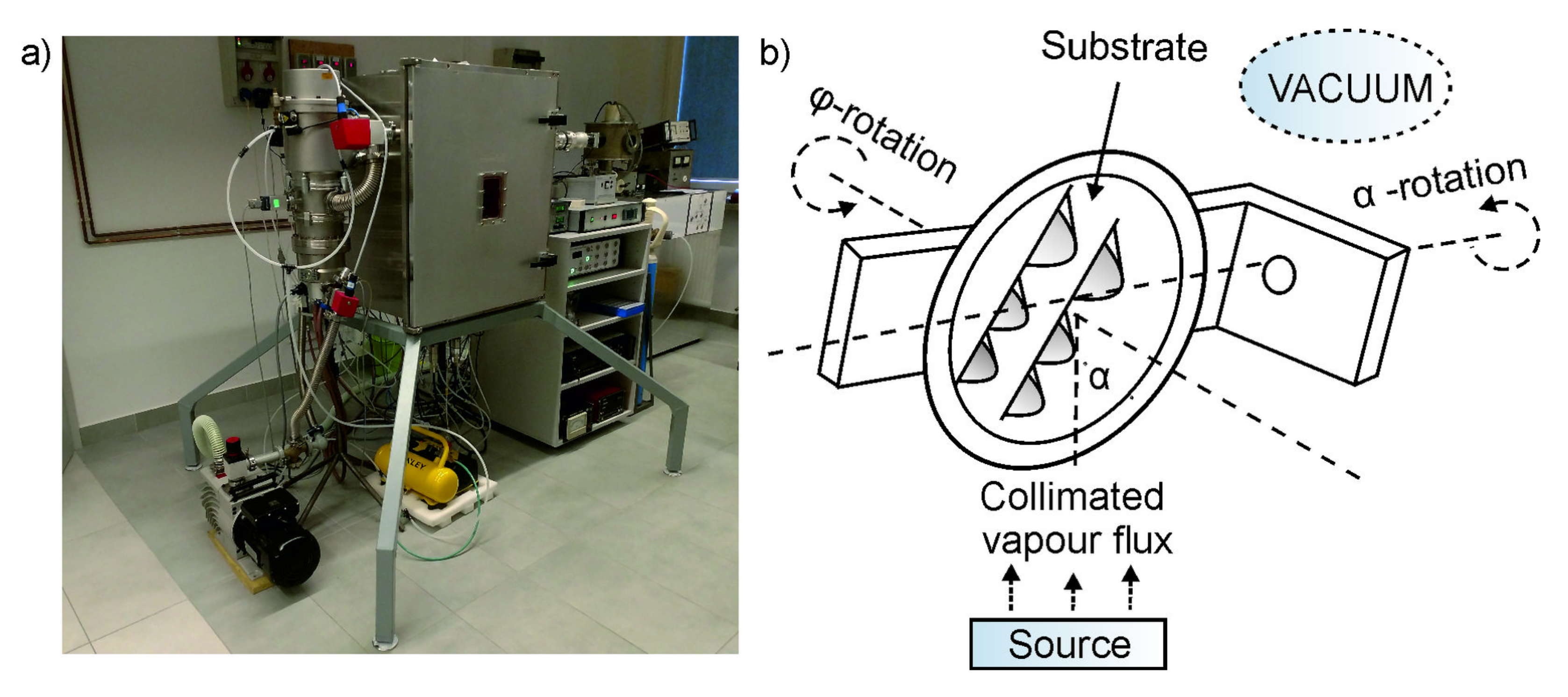
2.1. Tungsten Trioxide Deposition
2.2. XRD/XRR Measurements
2.3. AFM Measurements
2.4. Spectroscopic Ellipsometry Measurements
2.5. Gas-Sensing Measurements
3. Results
3.1. Characterization
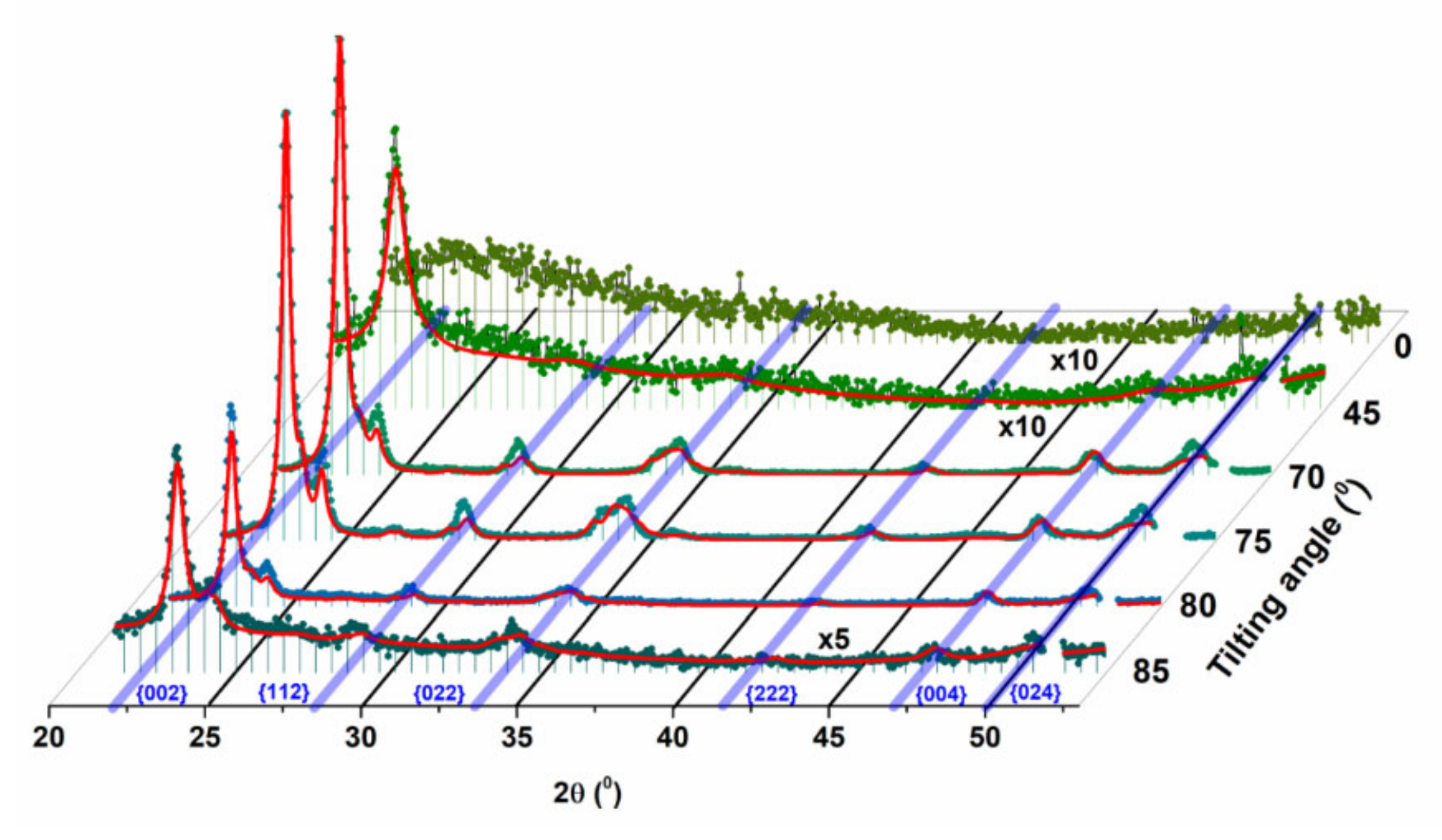
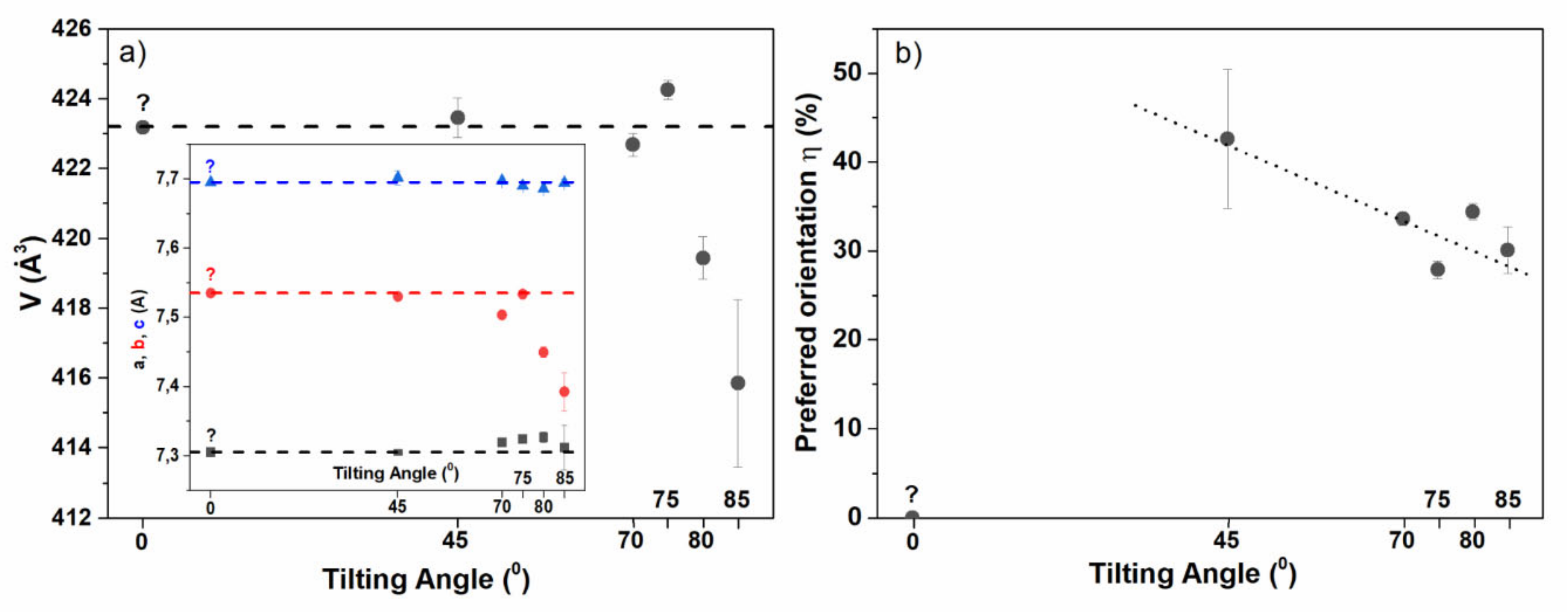
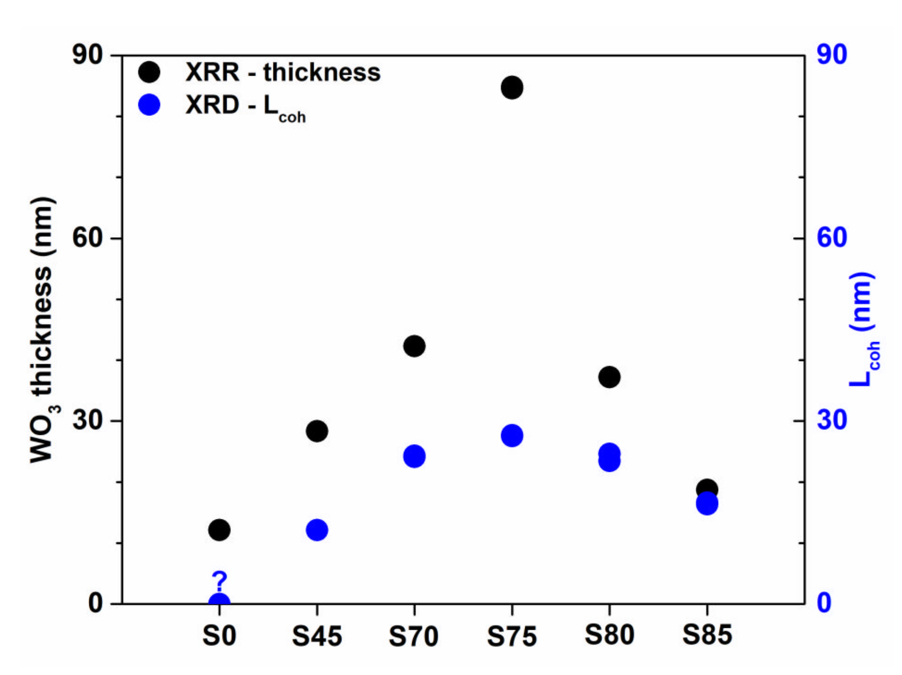
3.1.1. XRD/XRR
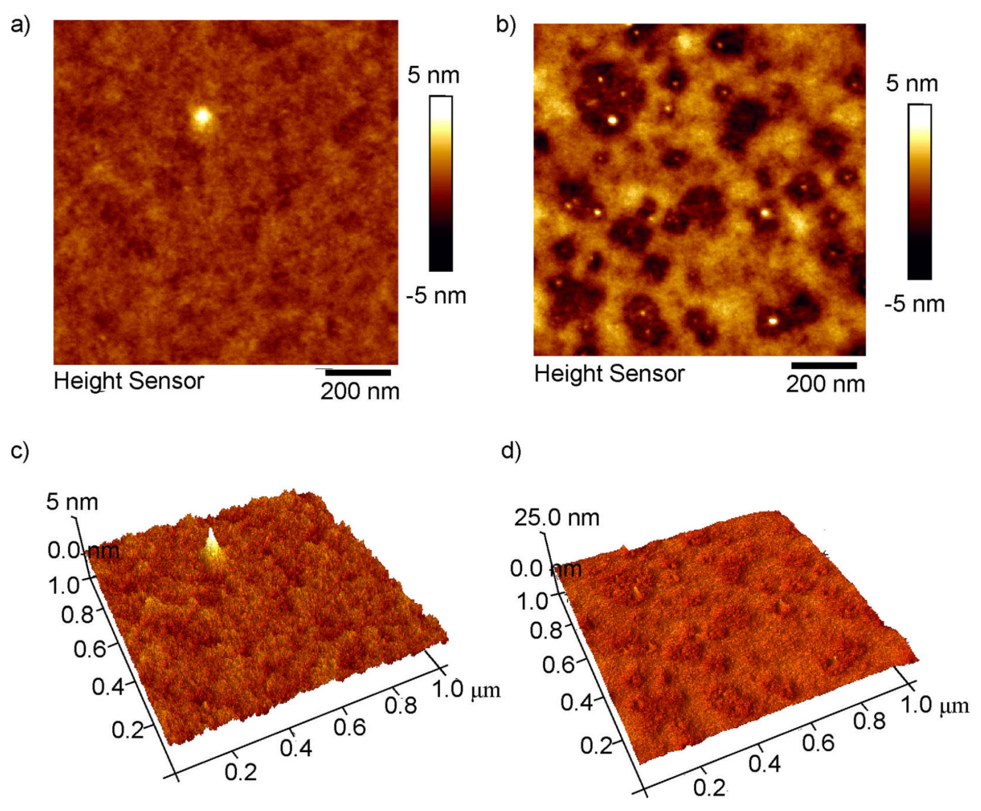
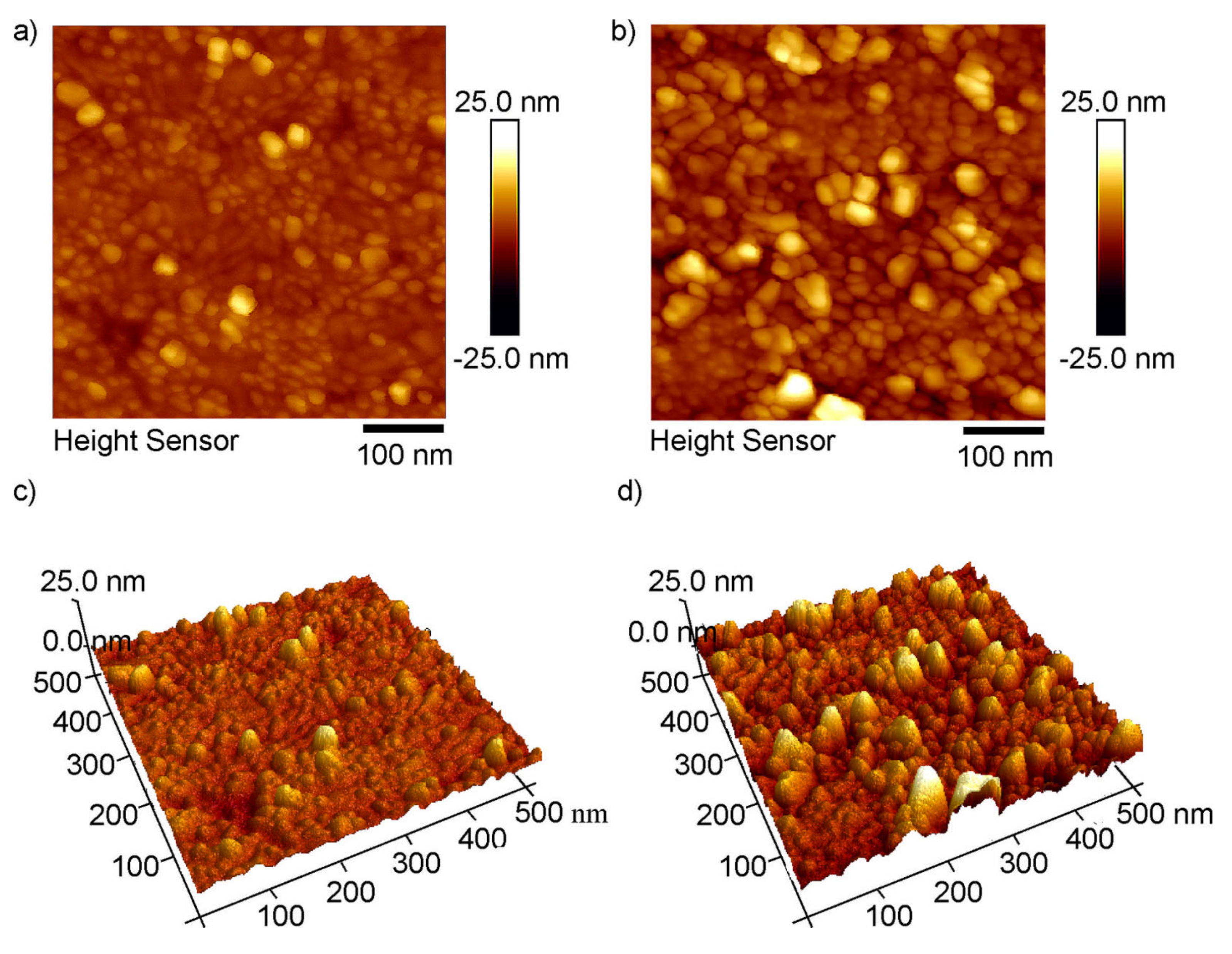
3.1.2. AFM
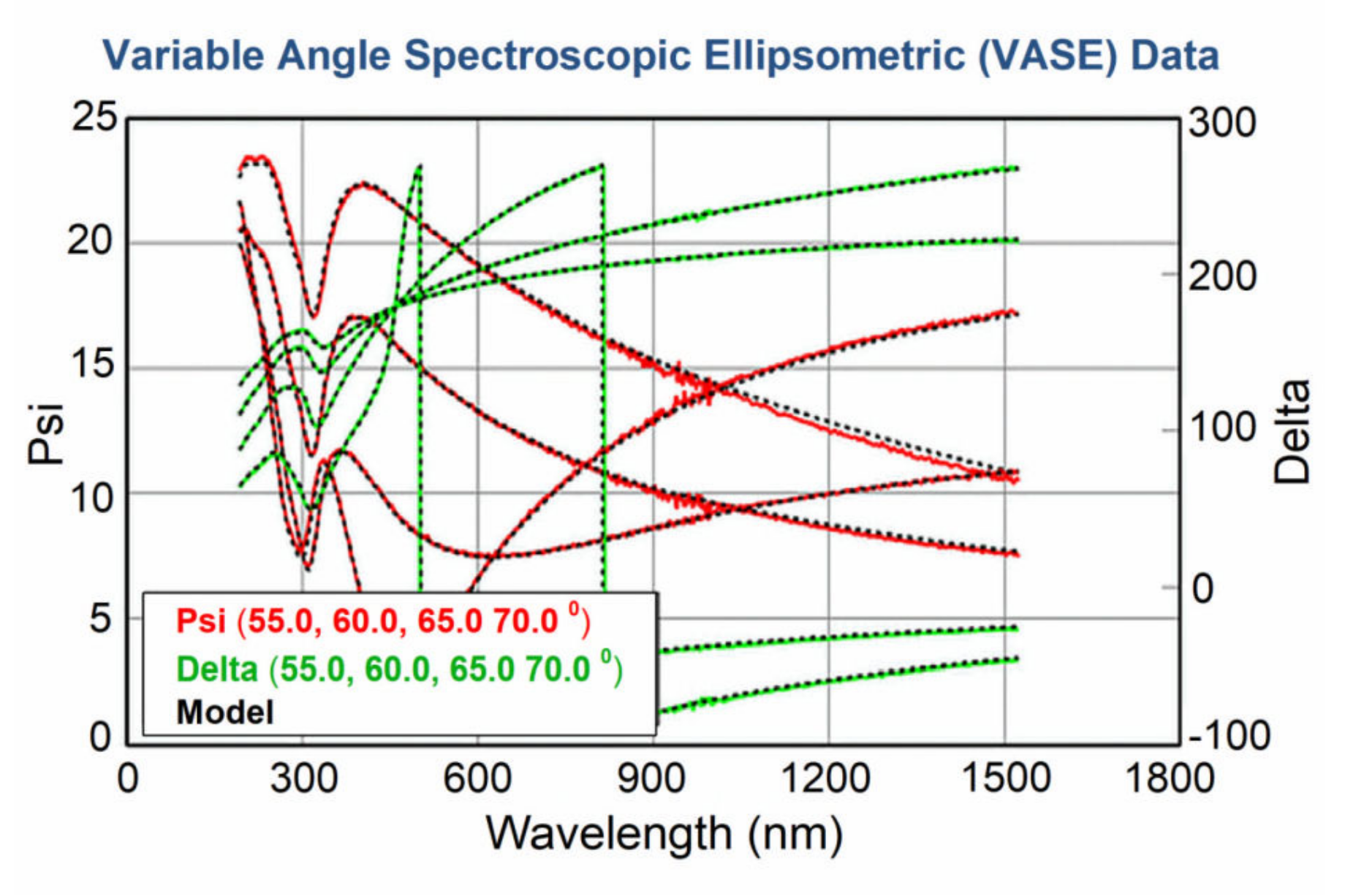
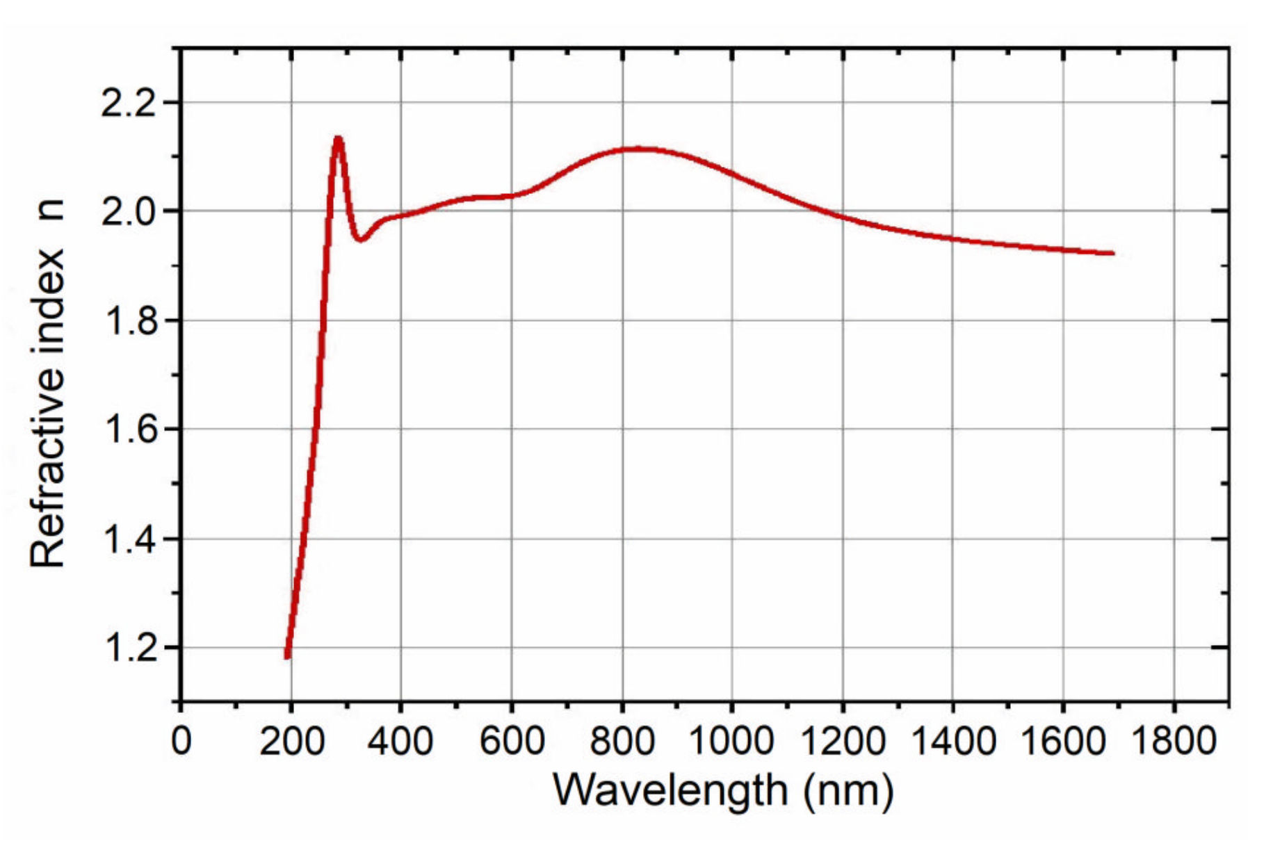
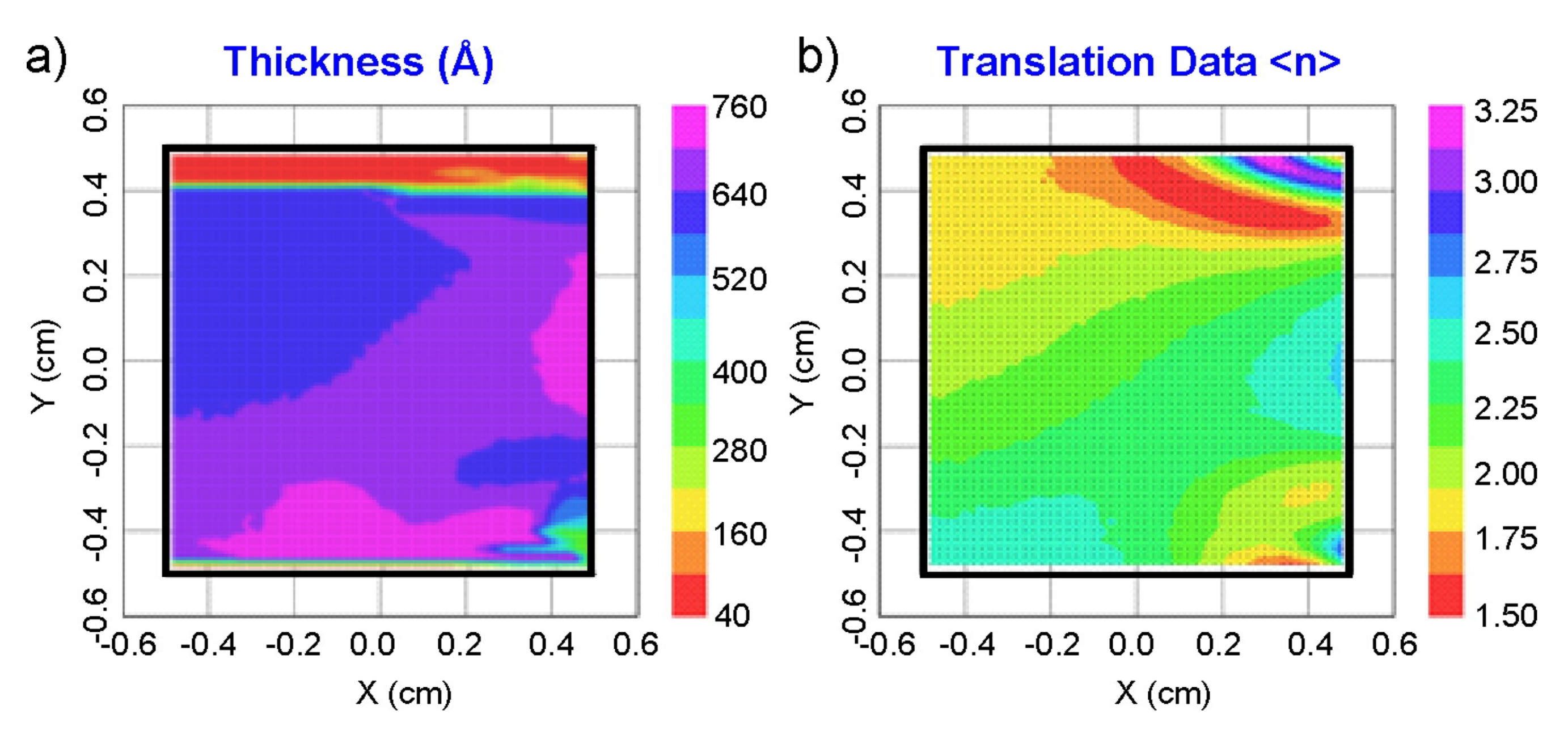
3.1.3. Spectroscopic Ellipsometry
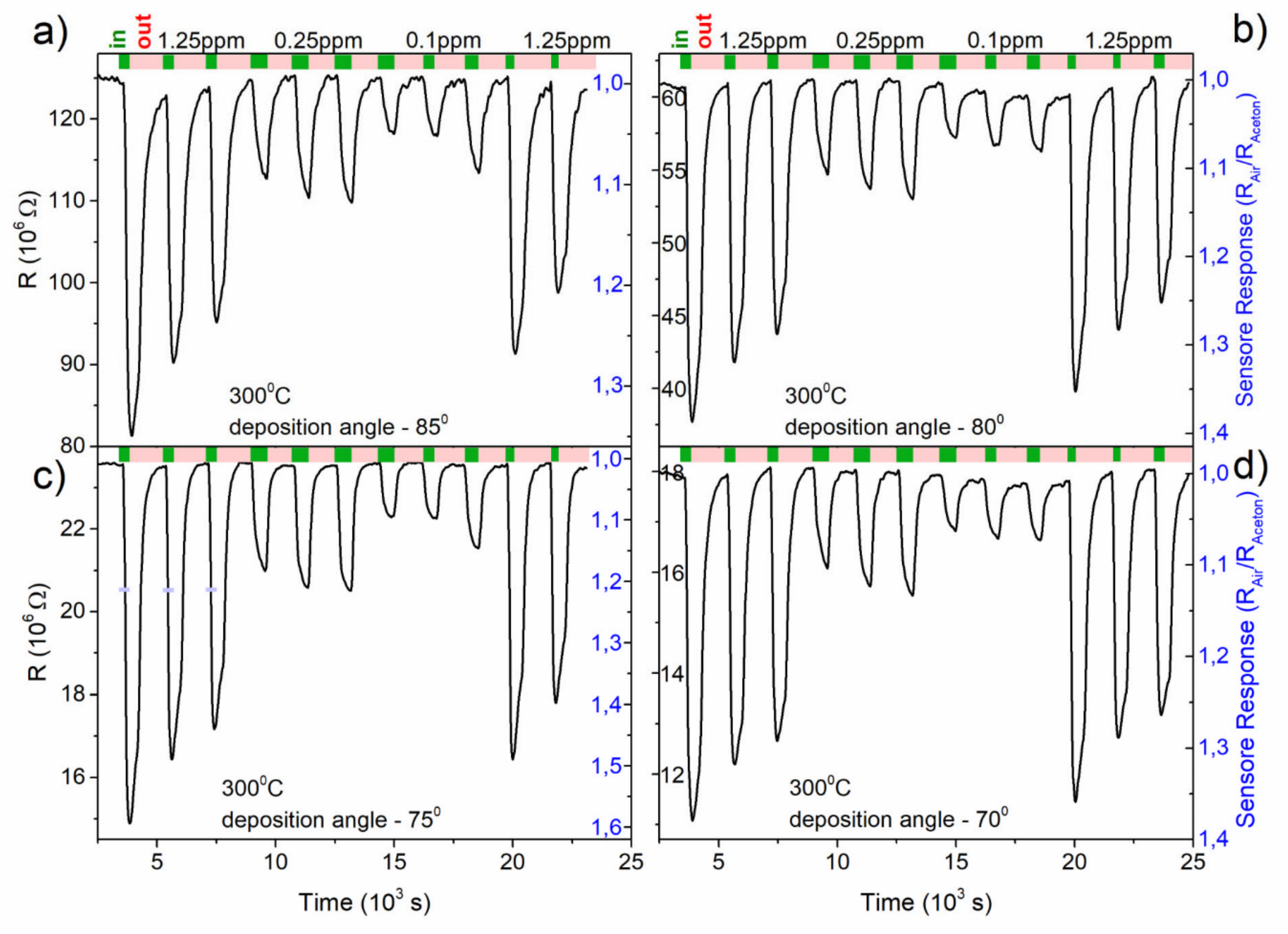
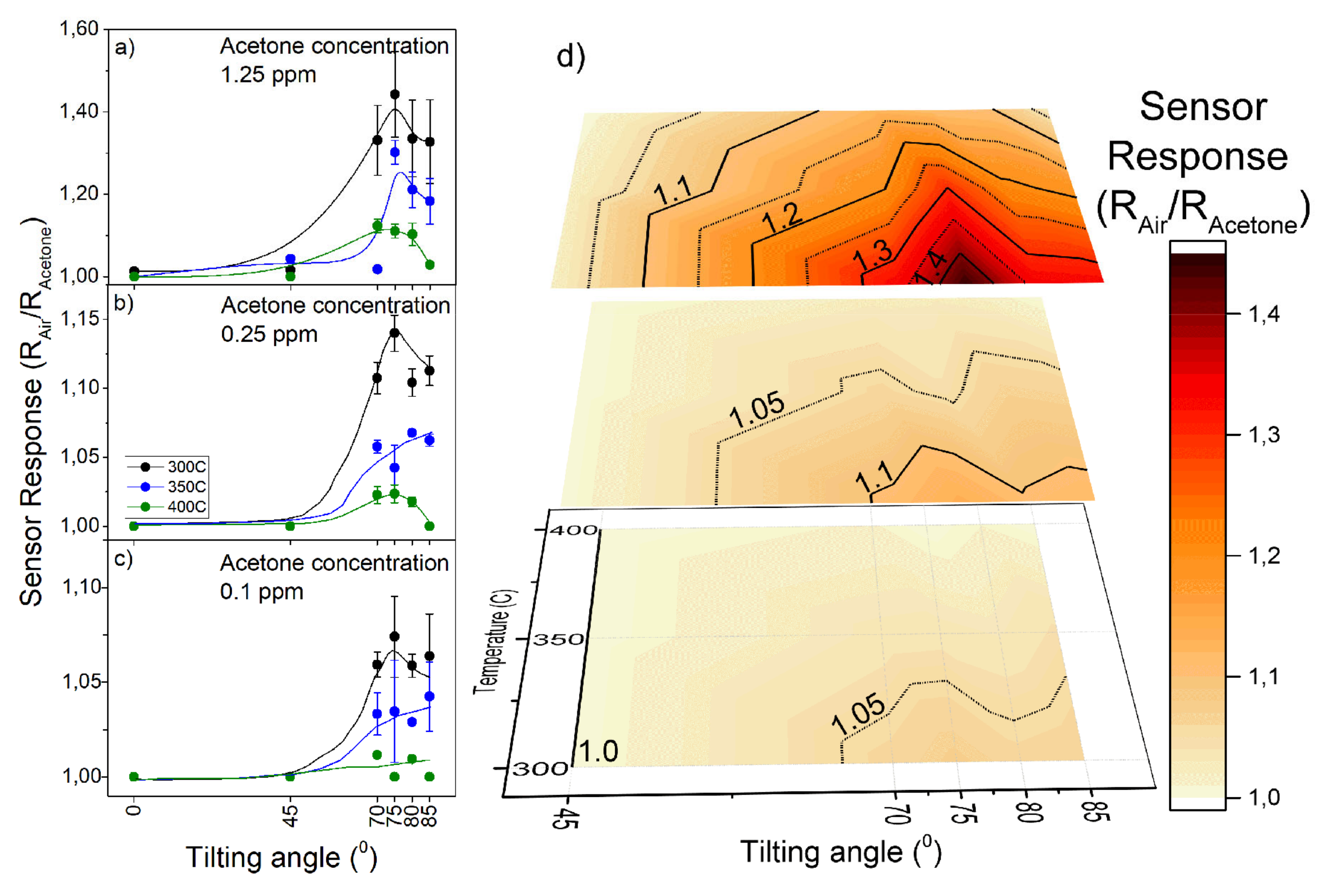
3.1.4. Gas-Sensing Characteristics
4. Conclusions
Author Contributions
Funding
Conflicts of Interest
Appendix A

| Sample | Omega (°) | a (Å) | b (Å) | c (Å) | V (Å3) | η (%) | Lcoh (nm) |
|---|---|---|---|---|---|---|---|
| S85 | 0.5 | 7.31(3) | 7.37(3) | 7.687(4) | 414.6(22) | 28.2(1) | 17.5 |
| 1. | 7.29(3) | 7.40(3) | 7.687(5) | 415.7(23) | 29.0(2) | 15.8 | |
| 3 | 7.33(4) | 7.40(2) | 7.696(6) | 417.3(26) | 33.2(2) | 16.7 | |
| mean | 7.31(3) | 7.39(3) | 7.690(5) | 415.8(24) | 30.1(2.6) | 16.6(9) | |
| S80 | 0.5 | 7.32(1) | 7.47() | 7.678(1) | 419.9(5) | 33.5(3) | 25.6 |
| 1. | 7.33(1) | 7.41(1) | 7.690(1) | 417.9(6) | 34.3(3) | 23.7 | |
| 3 | 7.33(1) | 7.46(1) | 7.609(1) | 420.5(7) | 35.5(3) | 24.5 | |
| mean | 7.33(1) | 7.45(1) | 7.686(1) | 419.4(13) | 34.4(9) | 24.6(9) | |
| S75 | 0.5 | 7.32(1) | 7.53(1) | 7.687(3) | 423.9(4) | 27.2(3) | 28.2 |
| 1. | 7.32(1) | 7.53(1) | 7.690(1) | 423.8(2) | 27.3(4) | 28.6 | |
| 3 | 7.33(1) | 7.53(1) | 7.696(1) | 425.0(2) | 29.0(4) | 25.9 | |
| mean | 7.32(1) | 7.53(1) | 7.690(2) | 424.3(6) | 27.9(1.0) | 27.5(15) | |
| S70 | 0.5 | 7.32(1) | 7.51(1) | 7.697(1) | 422.7(3) | 32.9(3) | 25.1 |
| 1. | 7.32(1) | 7.51(1) | 7.670(1) | 423.5(3) | 33.5(3) | 24.7 | |
| 3 | 7.32(1) | 7.49(1) | 7.696(1) | 421.9(4) | 34.4(4) | 23.15 | |
| mean | 7.32(1) | 7.50(1) | 7.697(1) | 422.7(8) | 33.6(7) | 24.3(11) | |
| S45 | 0.5 | 7.305 | 7.535 | 7.70(1) | 423.5(5) | 12.2 | |
| 1. | 7.305 | 7.535 | 7.70(1) | 423.1(5) | 12.7 | ||
| 3 | 7.305 | 7.535 | 7.71(1) | 423.8(7) | 11.7 | ||
| mean | 7.305 | 7.535 | 7.70(1) | 423.5(6) | 12.2(5) | ||
| S0 | Amorphous | - | - | - | - | - | - |
References
- Okamoto, H.; Schlesinger, M.E.; Mueller, E.M. (Eds.) Alloy Phase Diagrams; ASM International: Novelty, OH, USA, 2016; ISBN 978-1-62708-163-4. [Google Scholar]
- Hai, Z.; Wei, Z.; Xue, C.; Xu, H.; Verpoort, F. Nanostructured tungsten oxide thin film devices: From optoelectronics and ionics to iontronics. J. Mater. Chem. C 2019, 7, 12968–12990. [Google Scholar] [CrossRef]
- Mardare, C.C.; Hassel, A.W. Review on the Versatility of Tungsten Oxide Coatings. Phys. Status Solidi 2019, 216, 1900047. [Google Scholar] [CrossRef]
- Svensson, J.S.E.M.; Granqvist, C.G. Modulated transmittance and reflectance in crystalline electrochromic WO3 films: Theoretical limits. Appl. Phys. Lett. 1984, 45, 828–830. [Google Scholar] [CrossRef]
- Marszalek, K. Magnetron-sputtered WO3 films for electrochromic devices. Thin Solid Film. 1989, 175, 227–233. [Google Scholar] [CrossRef]
- Xu, J.; Ding, T.; Wang, J.; Zhang, J.; Wang, S.; Chen, C.; Fang, Y.; Wu, Z.; Huo, K.; Dai, J. Tungsten Oxide Nanofibers Self-assembled Mesoscopic Microspheres as High-performance Electrodes for Supercapacitor. Electrochim. Acta 2015, 174, 728–734. [Google Scholar] [CrossRef]
- Wang, Z.; Gong, W.; Wang, X.; Chen, Z.; Chen, X.; Chen, J.; Sun, H.; Song, G.; Cong, S.; Geng, F.; et al. Remarkable Near-Infrared Electrochromism in Tungsten Oxide Driven by Interlayer Water-Induced Battery-to-Pseudocapacitor Transition. ACS Appl. Mater. Interfaces 2020, 12, 33917–33925. [Google Scholar] [CrossRef]
- Yang, P.; Sun, P.; Du, L.; Liang, Z.; Xie, W.; Cai, X.; Huang, L.; Tan, S.; Mai, W. Quantitative Analysis of Charge Storage Process of Tungsten Oxide that Combines Pseudocapacitive and Electrochromic Properties. J. Phys. Chem. C 2015, 119, 16483–16489. [Google Scholar] [CrossRef]
- Singh, S.; Moudgil, A.; Mishra, N.; Das, S.; Mishra, P. Vancomycin functionalized WO3 thin film-based impedance sensor for efficient capture and highly selective detection of Gram-positive bacteria. Biosens. Bioelectron. 2019, 136, 23–30. [Google Scholar] [CrossRef] [PubMed]
- Santos, L.; Silveira, C.M.; Elangovan, E.; Neto, J.P.; Nunes, D.; Pereira, L.; Martins, R.; Viegas, J.; Moura, J.J.G.; Todorovic, S.; et al. Synthesis of WO3 nanoparticles for biosensing applications. Sens. Actuators B Chem. 2016, 223, 186–194. [Google Scholar] [CrossRef]
- Staerz, A.; Somacescu, S.; Epifani, M.; Russ, T.; Weimar, U.; Barsan, N. WO3 Based Gas Sensors. Proceedings 2019, 2, 826. [Google Scholar] [CrossRef]
- Dong, C.; Zhao, R.; Yao, L.; Ran, Y.; Zhang, X.; Wang, Y. A review on WO3 based gas sensors: Morphology control and enhanced sensing properties. J. Alloys Compd. 2020, 820, 153194. [Google Scholar] [CrossRef]
- Malik, R.; Tomer, V.K.; Mishra, Y.K.; Lin, L. Functional gas sensing nanomaterials: A panoramic view. Appl. Phys. Rev. 2020, 7, 21301. [Google Scholar] [CrossRef]
- Staerz, A.; Weimar, U.; Barsan, N. Understanding the Potential of WO3 Based Sensors for Breath Analysis. Sensors 2016, 16, 1815. [Google Scholar] [CrossRef]
- Rydosz, A. Sensors for Enhanced Detection of Acetone as a Potential Tool for Noninvasive Diabetes Monitoring. Sensors 2018, 18, 2298. [Google Scholar] [CrossRef]
- Rydosz, A.; Szkudlarek, A.; Ziabka, M.; Domanski, K.; Maziarz, W.; Pisarkiewicz, T. Performance of Si-Doped WO3 Thin Films for Acetone Sensing Prepared by Glancing Angle DC Magnetron Sputtering. IEEE Sens. J. 2016, 16, 1004–1012. [Google Scholar] [CrossRef]
- Rydosz, A. The Use of Copper Oxide Thin Films in Gas-Sensing Applications. Coatings 2018, 8, 425. [Google Scholar] [CrossRef]
- Andrysiewicz, W.; Krzeminski, J.; Skarżynski, K.; Marszalek, K.; Sloma, M.; Rydosz, A. Flexible Gas Sensor Printed on a Polymer Substrate for Sub-ppm Acetone Detection. Electron. Mater. Lett. 2020, 16, 146–155. [Google Scholar] [CrossRef]
- Saasa, V.; Lemmer, Y.; Malwela, T.; Akande, A.; Beukes, M.; Mwakikunga, B. Effect of varying ethanol and water compositions on the acetone sensing properties of WO3 for application in diabetes mellitus monitoring. Mater. Res. Express 2020, 7, 35905. [Google Scholar] [CrossRef]
- Lu, J.; Xu, C.; Cheng, L.; Jia, N.; Huang, J.; Li, C. Acetone sensor based on WO3 nanocrystallines with oxygen defects for low concentration detection. Mater. Sci. Semicond. Process. 2019, 101, 214–222. [Google Scholar] [CrossRef]
- Wei, S.; Zhao, G.; Du, W.; Tian, Q. Synthesis and excellent acetone sensing properties of porous WO3 nanofibers. Vacuum 2016, 124, 32–39. [Google Scholar] [CrossRef]
- Shi, J.; Hu, G.; Sun, Y.; Geng, M.; Wu, J.; Liu, Y.; Ge, M.; Tao, J.; Cao, M.; Dai, N. WO3 nanocrystals: Synthesis and application in highly sensitive detection of acetone. Sens. Actuators B Chem. 2011, 156, 820–824. [Google Scholar] [CrossRef]
- Chi, X.; Liu, C.; Liu, L.; Li, Y.; Wang, Z.; Bo, X.; Liu, L.; Su, C. Tungsten trioxide nanotubes with high sensitive and selective properties to acetone. Sens. Actuators B Chem. 2014, 194, 33–37. [Google Scholar] [CrossRef]
- Kaur, J.; Anand, K.; Anand, K.; Singh, R.C. WO3 nanolamellae/reduced graphene oxide nanocomposites for highly sensitive and selective acetone sensing. J. Mater. Sci. 2018, 53, 12894–12907. [Google Scholar] [CrossRef]
- Shen, J.Y.; Wang, M.D.; Wang, Y.F.; Hu, J.Y.; Zhu, Y.; Zhang, Y.X.; Li, Z.J.; Yao, H.C. Iron and carbon codoped WO3 with hierarchical walnut-like microstructure for highly sensitive and selective acetone sensor. Sens. Actuators B Chem. 2018, 256, 27–37. [Google Scholar] [CrossRef]
- Righettoni, M.; Tricoli, A.; Gass, S.; Schmid, A.; Amann, A.; Pratsinis, S.E. Breath acetone monitoring by portable Si:WO3 gas sensors. Anal. Chim. Acta 2012, 738, 69–75. [Google Scholar] [CrossRef]
- Li, Y.; Hua, Z.; Wu, Y.; Zeng, Y.; Qiu, Z.; Tian, X.; Wang, M.; Li, E. Modified impregnation synthesis of Ru-loaded WO3 nanoparticles for acetone sensing. Sens. Actuators B Chem. 2018, 265, 249–256. [Google Scholar] [CrossRef]
- Xu, Y.; Lou, C.; Zheng, L.; Zheng, W.; Liu, X.; Kumar, M.; Zhang, J. Highly sensitive and selective detection of acetone based on platinum sensitized porous tungsten oxide nanospheres. Sens. Actuators B Chem. 2020, 307, 127616. [Google Scholar] [CrossRef]
- Xu, Y.; Ma, T.; Zheng, L.; Zhao, Y.; Liu, X.; Zhang, J. Heterostructures of hematite-sensitized W18O49 hollow spheres for improved acetone detection with ultralow detection limit. Sens. Actuators B Chem. 2019, 288, 432–441. [Google Scholar] [CrossRef]
- Xiao, T.; Wang, X.Y.; Zhao, Z.H.; Li, L.; Zhang, L.; Yao, H.C.; Wang, J.S.; Li, Z.J. Highly sensitive and selective acetone sensor based on C-doped WO3 for potential diagnosis of diabetes mellitus. Sens. Actuators B Chem. 2014, 199, 210–219. [Google Scholar] [CrossRef]
- Wang, M.D.; Li, Y.Y.; Yao, B.H.; Zhai, K.; Li, Z.J.; Yao, H.C. Synthesis of three-dimensionally ordered macro/mesoporous C-doped WO3 materials: Effect of template sizes on gas sensing properties. Sens. Actuators B Chem. 2019, 288, 656–666. [Google Scholar] [CrossRef]
- Liang, Y.C.; Chao, Y. Enhancement of Acetone Gas-Sensing Responses of Tapered WO3 Nanorods through Sputtering Coating with a Thin SnO2 Coverage Layer. Nanomaterials 2019, 9, 864. [Google Scholar] [CrossRef] [PubMed]
- Xu, W.; Qiu, C.; Zhou, J.; Chen, Y. Regulation of specific surface area of 3D flower-like WO3 hierarchical structures for gas sensing application. Ceram. Int. 2020, 46, 11372–11378. [Google Scholar] [CrossRef]
- Wei, Z.; Xu, L.; Peng, S.; Zhou, Q. Application of WO3 Hierarchical Structures for the Detection of Dissolved Gases in Transformer Oil: A Mini Review. Front. Chem. 2020, 8. [Google Scholar] [CrossRef]
- Hawkeye, M.M.; Taschuk, M.T.; Brett, M.J. Glancing Angle Deposition of Thin Films; John Wiley & Sons, Ltd.: Chichester, UK, 2014; ISBN 9781118847510. [Google Scholar]
- Hawkeye, M.M.; Brett, M.J. Glancing angle deposition: Fabrication, properties, and applications of micro- and nanostructured thin films. J. Vac. Sci. Technol. A Vac. Surf. Film. 2007, 25, 1317. [Google Scholar] [CrossRef]
- Bales, G.S.; Bruinsma, R.; Eklund, E.A.; Karunasiri, R.P.U.; Rudnick, J.; Zangwill, A. Growth and Erosion of Thin Solid Films. Science 1990, 249, 264–268. [Google Scholar] [CrossRef] [PubMed]
- Vick, D.; Smy, T.; Brett, M.J. Growth behavior of evaporated porous thin films. J. Mater. Res. 2002, 17, 2904–2911. [Google Scholar] [CrossRef]
- Siewert, J.M.A.; LaForge, J.M.; Taschuk, M.T.; Brett, M.J. Disassembling Glancing Angle Deposited Films for High-Throughput, Single-Post Growth Scaling Measurements. Microsc. Microanal. 2012, 18, 1135–1142. [Google Scholar] [CrossRef]
- Robbie, K.; Brett, M.J. Sculptured thin films and glancing angle deposition: Growth mechanics and applications. J. Vac. Sci. Technol. A Vac. Surf. Film. 1997, 15, 1460–1465. [Google Scholar] [CrossRef]
- Siad, A.; Besnard, A.; Nouveau, C.; Jacquet, P. Critical angles in DC magnetron glad thin films. Vacuum 2016, 131, 305–311. [Google Scholar] [CrossRef]
- Smith, W.; Zhang, Z.Y.Y.; Zhao, Y.P.P. Structural and optical characterization of WO3 nanorods/films prepared by oblique angle deposition. J. Vac. Sci. Technol. B Microelectron. Nanom. Struct. 2007, 25, 1875. [Google Scholar] [CrossRef]
- Yuan, J.; Wang, B.; Wang, H.; Chai, Y.; Jin, Y.; Qi, H.; Shao, J. Electrochromic behavior of WO3 thin films prepared by GLAD. Appl. Surf. Sci. 2018, 447, 471–478. [Google Scholar] [CrossRef]
- Wisitsoorat, A.; Ahmad, M.Z.; Yaacob, M.H.; Horpratum, M.; Phakaratkul, D.; Lomas, T.; Tuantranont, A.; Wlodarski, W. Optical H2 sensing properties of vertically aligned Pd/WO3 nanorods thin films deposited via glancing angle rf magnetron sputtering. Sens. Actuators B Chem. 2013, 182, 795–801. [Google Scholar] [CrossRef]
- Ollitrault, J.; Martin, N.; Rauch, J.Y.; Sanchez, J.B.; Berger, F. Improvement of ozone detection with GLAD WO3 films. Mater. Lett. 2015, 155, 1–3. [Google Scholar] [CrossRef]
- Xu, X.; Arab Pour Yazdi, M.; Sanchez, J.B.; Billard, A.; Berger, F.; Martin, N. Reactive co-sputtering of tungsten oxide thin films by glancing angle deposition for gas sensors. Mater. Today Proc. 2019, 6, 314–318. [Google Scholar] [CrossRef]
- Ahmad, M.Z.; Wisitsoraat, A.; Zoolfakar, A.S.; Kadir, R.A.; Wlodarski, W. Investigation of RF sputtered tungsten trioxide nanorod thin film gas sensors prepared with a glancing angle deposition method toward reductive and oxidative analytes. Sens. Actuators B Chem. 2013, 183, 364–371. [Google Scholar] [CrossRef]
- Rydosz, A.; Dyndał, K.; Andrysiewicz, W.; Grochala, D.; Marszałek, K. GLAD Magnetron Sputtered Ultra-Thin Copper Oxide Films for Gas-Sensing Application. Coatings 2020, 10, 378. [Google Scholar] [CrossRef]
- Rodríguez-Carvajal, J. Recent developments of the program FULLPROF. Newsl. Comm. Powder Diffr. 2001, 26, 12–19. [Google Scholar]
- Zolotoyabko, E. Determination of the degree of preferred orientation within the March-Dollase approach. J. Appl. Crystallogr. 2009, 42, 513–518. [Google Scholar] [CrossRef]
- Perzanowski, M.; Zabila, Y.; Krupinski, M.; Zarzycki, A.; Polit, A.; Marszalek, M. Chemical order and crystallographic texture of FePd:Cu thin alloy films. J. Appl. Phys. 2012, 111, 74301. [Google Scholar] [CrossRef]
- Charles, C.; Martin, N.; Devel, M.; Ollitrault, J.; Billard, A. Correlation between structural and optical properties of WO3 thin films sputter deposited by glancing angle deposition. Thin Solid Film. 2013, 534, 275–281. [Google Scholar] [CrossRef]
- Rydosz, A.; Dyndał, K.; Kollbek, K.; Andrysiewicz, W.; Sitarz, M.; Marszałek, K. Structure and optical properties of the WO3 thin films deposited by the GLAD magnetron sputtering technique. Vacuum 2020, 177, 109378. [Google Scholar] [CrossRef]


| WO3 Based Sensor (Fabrication Method) | Operating Temperature (°C) | Concentration (ppm) | Response (RAir/RGas) | Response/Recovery Time (s) | References |
|---|---|---|---|---|---|
| WO3 nanostructures (solvothermal) | 100 | 0.05–3.5 | ~120–700 | ~500/500 | [19] |
| WO3 nanocrystallites with oxygen defects (microwave-assisted hydrothermal method) | 320 | 0.25 100 | 3.8 31 | 4/5 | [20] |
| WO3 porous nanofibers (electrospinning) | 270 | 0.5–100 | ~3–60 | ~10/30 | [21] |
| WO3 nanocrystals (sol-gel) | 300 | 0.05–5 | ~1.2–7.5 | >30/>30 | [22] |
| WO3 nanotubes (electrospinning) | 250 | 0.5–100 | ~2.5–45 | 5/22 | [23] |
| WO3 nanolamella/reduced graphene oxide (hydrothermal) | 200 | 1–500 | ~1.75–30 | ~2/10 | [24] |
| Fe-C-codoped WO3 walnut-like microspheres (hydrothermal) | 300 | 0.2–10 | ~4.5–17.8 | ~50/65 | [25] |
| WO3:Si nanoparticles (flame spray pyrolysis reaction) | 350 | 0.1 0.5 | 1.5 2.75 | ~10/30 ~10/50 | [26] |
| WO3:Si thin film (reactive DC GLAD 80° sputtering) | 425 | 0.04–3.8 | 3–40.5 | ~60/150 | [16] |
| WO3 with Ru loaded nanoparticles (acidification + Ru impregnation) | 300 | 0.5–30 | ~1.5–4 ~6–85 (Ru) | ~720/3000 | [27] |
| W18O49 hollow porous spheres with Pt nanoparticles (hydrothermal reaction + atomic layer deposition of Pt) | 180 | 0.5, 20 | ~1.5, 2.1 ~2.5, 85 (Pt) | 13/11 8/26 | [28] |
| W18O49/α-Fe2O3 hollow porous spheres (hydrothermal) | 260 | 0.5–100 | ~1.6–13.8 | 10/30 | [29] |
| WO3:C nanoparticles decorating fiber (cotton fiber-template calcination) | 300 | 0.32–5 | 2–8 | 3/6–9/12 | [30] |
| WO3:C doped 3D mesoporous (colloidal crystal template) | 390 | 0.9–10 | ~6–13.5 | ~60/55 | [31] |
| WO3-SnO2 nanorodes (hydrothermal and sputtering) | 300 | 100–1000 | 6–12 | 3/28 | [32] |
| WO3 3D flower-like nanostructures (hydrothermal) | 350 | 35 | 22 | - | [33] |
Publisher’s Note: MDPI stays neutral with regard to jurisdictional claims in published maps and institutional affiliations. |
© 2020 by the authors. Licensee MDPI, Basel, Switzerland. This article is an open access article distributed under the terms and conditions of the Creative Commons Attribution (CC BY) license (http://creativecommons.org/licenses/by/4.0/).
Share and Cite
Zarzycki, A.; Dyndał, K.; Sitarz, M.; Xu, J.; Gao, F.; Marszałek, K.; Rydosz, A. Influence of GLAD Sputtering Configuration on the Crystal Structure, Morphology, and Gas-Sensing Properties of the WO3 Films. Coatings 2020, 10, 1030. https://doi.org/10.3390/coatings10111030
Zarzycki A, Dyndał K, Sitarz M, Xu J, Gao F, Marszałek K, Rydosz A. Influence of GLAD Sputtering Configuration on the Crystal Structure, Morphology, and Gas-Sensing Properties of the WO3 Films. Coatings. 2020; 10(11):1030. https://doi.org/10.3390/coatings10111030
Chicago/Turabian StyleZarzycki, Arkadiusz, Katarzyna Dyndał, Maciej Sitarz, Jie Xu, Feng Gao, Konstanty Marszałek, and Artur Rydosz. 2020. "Influence of GLAD Sputtering Configuration on the Crystal Structure, Morphology, and Gas-Sensing Properties of the WO3 Films" Coatings 10, no. 11: 1030. https://doi.org/10.3390/coatings10111030
APA StyleZarzycki, A., Dyndał, K., Sitarz, M., Xu, J., Gao, F., Marszałek, K., & Rydosz, A. (2020). Influence of GLAD Sputtering Configuration on the Crystal Structure, Morphology, and Gas-Sensing Properties of the WO3 Films. Coatings, 10(11), 1030. https://doi.org/10.3390/coatings10111030