Article

Ti–Cu Coatings Deposited by a Combination of HiPIMS and DC Magnetron Sputtering: The Role of Vacuum Annealing on Cu Diffusion, Microstructure, and Corrosion Resistance

1
Key Laboratory for Advanced Technologies of Materials, Ministry of Education, School of Materials Science and Engineering, Southwest Jiaotong University, Chengdu 610031, China
2
College of Physics and Engineering, Chengdu Normal University, Chengdu 611130, China
3
School of Biomedical Engineering, University of Sydney, Sydney, NSW 2006, Australia
4
School of Physics, University of Sydney, Sydney, NSW 2006, Australia
5
Sydney Nano Institute, University of Sydney, Sydney, NSW 2006, Australia
*
Authors to whom correspondence should be addressed.
Coatings 2020, 10(11), 1064; https://doi.org/10.3390/coatings10111064
Submission received: 1 October 2020 / Revised: 24 October 2020 / Accepted: 31 October 2020 / Published: 5 November 2020
(This article belongs to the Special Issue Plasma Technologies for Surface Engineering)

Abstract

:
Titanium-copper (Ti–Cu) coatings have attracted extensive attention in the surface modification of industrial and biomedical materials due to their excellent physical and chemical properties and biocompatibility. Here, Ti–Cu coatings are fabricated using a combination of high-power pulsed magnetron sputtering (HPPMS; also known as high power impulse magnetron sputtering (HiPIMS)) and DC magnetron sputtering followed by vacuum annealing at varied temperatures (300, 400, and 500 °C). X-ray diffraction (XRD), transmission electron microscopy (TEM), and X-ray photoelectron spectroscopy (XPS) data showed that Ti, Cu, and CuTi3 are mainly formed in the coatings before annealing, while Ti3O, Cu2O, and CuTi3 are the main compounds present in the annealed coatings. The cross-sectional TEM micrographs and corresponding EDS results provided evidence that Ti is mainly present on the surface and interfaces of the silicon substrate and the Ti–Cu coatings annealed at 500 °C, while the bulk of the coatings is enriched with Cu. The resistivity of the coatings decreased with increasing the annealing temperature from 300 to 500 °C. Based on self-corrosion current density data, the Ti–Cu coating annealed at 300 °C showed similar corrosion performance compared to the as-deposited Ti–Cu coating, while the corrosion rate increased for the Ti–Cu coatings annealed at 400 and 500 °C. Stable release of copper ions in PBS (cumulative released concentration of 0.8–1.0 μM) for up to 30 days was achieved for all the annealed coatings. Altogether, the results demonstrate that vacuum annealing is a simple and viable approach to tune the Cu diffusion and microstructure of the Ti–Cu coatings, thereby modulating their electrical resistivity, corrosion performance, and Cu ion release behavior.

1. Introduction

Titanium and titanium-based alloys have been widely used in industries such as chemical and biomedical engineering due to their corrosion resistance, mechanical properties, elasticity, excellent thermal and chemical stability, as well as biocompatibility [1,2,3,4]. Copper is used as a conductor of heat and electricity [5], antimicrobial material [6], building material [7], and constituent of various metal alloys [8,9,10]. Titanium combined with copper in the form of thin Ti–Cu coatings has potential applications in surface engineering of devices to modify their mechanical, anticorrosion and antibacterial properties, as well as biocompatibility [11,12,13,14,15]. Ti–Cu coatings show improved corrosion resistance compared to stainless steels (SS) substrates [14,16,17]. Copper ions can be released from the Cu-containing materials such as Cu, Cu alloys, Cu nanoparticles, CuS nanodots, copper(II)-chitosan complexes, copper phosphate cement, and Ti–Cu coatings, and therefore influence the antimicrobial functionality or cell behaviors [18,19,20,21,22].
Vacuum annealing is a common method to change the microstructure, corrosion behavior, resistivity, mechanical properties and biocompatibility of materials [23,24]. It has been reported that annealing of Ti–Cu coatings with Ti concentration of 1.3 and 2.9 at.% in an argon atmosphere results in the segregation of the top and bottom of the coating, forming a supersaturated Ti layer suitable for self-forming barrier layers in integrated circuits [25].
There is limited knowledge available in the literature on the effect of vacuum annealing on corrosion performance and Cu ion release behavior of Ti–Cu coatings. The microstructure evaluated by high-resolution transmission electron microscopy (HRTEM) and selective area electron diffraction (SAED) is also rarely reported for annealed Ti–Cu coatings. In the present paper, Ti–Cu coatings were prepared using a combination of HiPIMS and DCMS sputtering techniques. The sputtering material is highly ionized in the HiPIMS process; therefore, facilitating the fabrication of high density, homogenous, and smooth coatings with superior substrate–coating adhesion [26,27,28,29,30]. Following the deposition of the coatings, they were vacuum annealed at various temperatures ranging from 300 to 500 °C. The effect of vacuum annealing on elemental composition and distribution; chemical state; microstructure; as well as the resistivity, corrosion properties, and Cu ion release profiles of Ti–Cu coatings was evaluated.

2. Materials and Methods

Ti–Cu coatings were fabricated on silicon and 316L SS by co-sputtering using high power pulsed magnetron sputtering (HPPMS) and DC magnetron sputtering (DCMS) according to our previous paper [16]. Silicon (100) wafers with arithmetical mean roughness (Ra) of approximately 0.5 nm were purchased from Emei Semiconductor (Leshan, China). 316L SS substrates were polished to a mirror-like surface. Copper and titanium targets with the dimensions of 170 mm × 135 mm × 10 mm (99.9 at.% purity) were sputtered using DC (sputtering current: 2 A) and HiPIMS power supplies (voltage: −600 V; frequency: 100 Hz; pulse width: 50 µs), respectively. The base pressure in the chamber was approximately 2.0 × 10⁻³ Pa. Before deposition, the copper and titanium targets were pre-sputtered using a 2 A DC power supply for 10 min to etch the targets’ surface oxide layer. The silicon (100) and 316L SS substrates were cleaned using argon ion sputtering with a negative bias voltage of 1500 V at 3 Pa for 15 min. The distance between the substrate and target of Ti and Cu was 140 and 180 mm, respectively. The substrates were not heated during the deposition runs. A bias voltage of −50 V was applied to the substrate holder. The pressure of argon gas was 0.6 Pa and deposition time was 10 min.
The deposited Ti–Cu coatings were vacuum annealed using MFAD500 magnetic filter metal arc deposition equipment. The samples were placed in the vacuum chamber at the temperatures of 300, 400, and 500 °C for 30 min. The base pressure was less than 1.0 × 10⁻³ Pa. The samples in the chamber were cooled to room temperature in a consistent manner. The Ti–Cu coatings annealed at the temperatures of 300, 400, and 500 °C are named as Ti–Cu-300 °C, Ti–Cu-400 °C, and Ti–Cu-500 °C, respectively.
The surface morphology of the as-deposited and annealed Ti–Cu coatings was evaluated using scanning electron microscopy (JSM-7800F, JEOL, Tokyo, Japan) equipped with energy dispersive X-ray spectroscopy (EDS, OXFORD, Abingdon, UK). The phase structure of the deposited and annealed Ti–Cu coatings was investigated via X-ray diffraction equipment (Philips X’pert, Amsterdam, Holland) equipped with Cu Kα radiation (λ = 1.5406 Å) at 30 mA and 30 kV in the 2θ range of 30–50°. The microstructure of Ti–Cu coatings before and after annealing was further characterized by transmission electron microscopy (FEI Titan G2 60-300 (AC-TEM), Hillsboro, OR, USA) at the acceleration voltage of 300 kV. X-ray Photoelectron Spectroscopy (Escalab 250Xi, Waltham, MA, USA) measurements were carried out to determine the chemistry of the Ti–Cu coatings before and after Ar+ ion sputtering. The X-ray source (Al Kα, 1486.86 eV) was operating at 12.5 kV and 16 mA. The surfaces were etched using an Ar+ ion source with an etching rate of approximately 1 nm/s. The ion gun current was 10 A and the etching angle was 30°.
The electrical resistivity of the Ti–Cu coatings before and after annealing was calculated at room temperature using a four-point probe (SZ-82, Suzhou, China). The size of the samples was 1 × 3 cm2, and 5 positions on the surfaces of the sample were tested to calculate the average values of the resistivity.
The electrochemical corrosion properties of the Ti–Cu coatings before and after annealing were evaluated using an electrochemical workstation (IM6, Zahner, Kronach, Germany). The phosphate buffer solution (PBS) with pH of 7.4 was employed as the electrolyte solution. The scanning range was from −0.8 to 0.8 V and the scanning rate was 1 mV/s. A scanning electron microscope (JSM-7000 1F) was used to evaluate the surface morphology of the samples after the electrochemical corrosion tests.
The concentration of Cu ions released from the Ti–Cu coatings before and after annealing was measured using an inductively coupled plasma mass spectrometry (ICP-MS, Agilent 7700, Santa Clara, CA, USA) with an accuracy of 0.005 mg/L. The coatings were soaked in 10 mL of PBS (pH = 7.4) for 30 min, 1 d, 3 d, 7 d, 15 d and 30 d at 37 °C in a thermostat water bath, and then the concentration of Cu ions was measured.

3. Results and Discussion

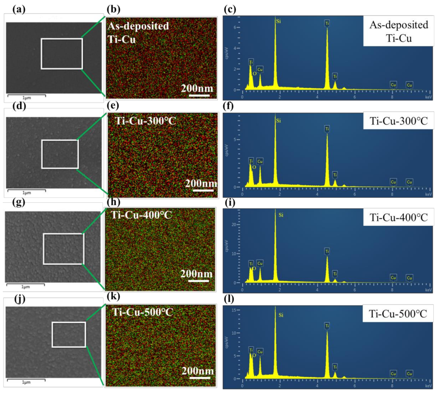
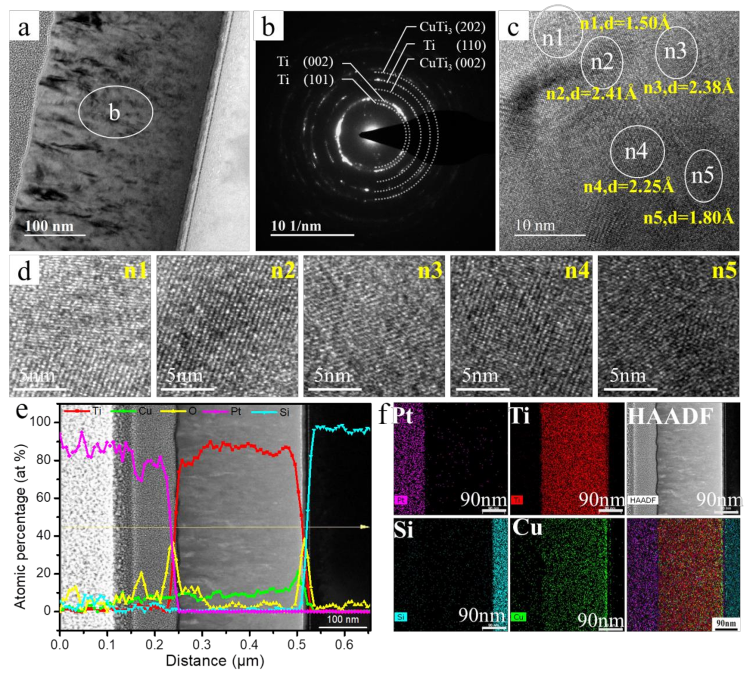
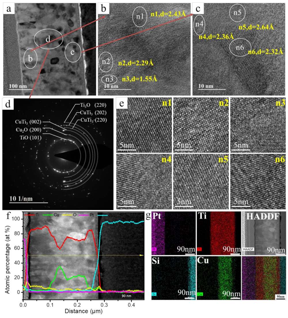
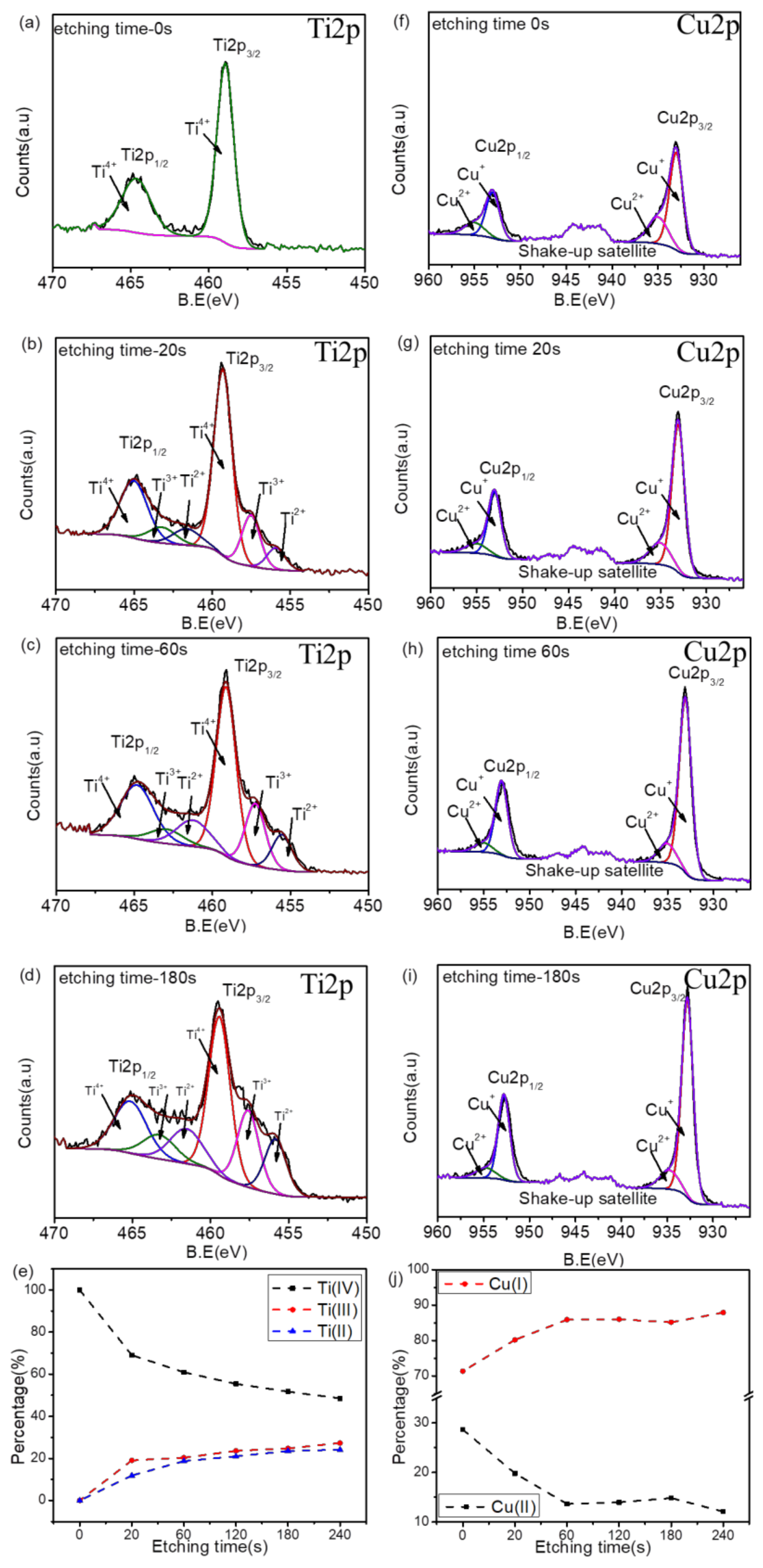
3.1. Surface Chemistry and Structural Analyses of Ti–Cu Coatings

The copper contents of Ti–Cu coatings deposited on silicon substrates before and after annealing treatment were evaluated through EDS mapping. The ratio of Cu/(Cu + Ti) atomic concentrations obtained from EDS analysis are listed in Table 1, and the surface elemental distribution on the Ti–Cu coatings evaluated by EDS mapping (Ti: red points; Cu: green points) are shown in Figure 1b,e,h,k. As observed, the distribution of Cu is relatively uniform for the Ti–Cu coatings for both before and after annealing conditions. The sampling depth of EDS is in the range of micrometers [31,32], which is much larger than the thickness of the Ti–Cu coatings that was approximately 250 nm, as evaluated by cross-sectional TEM images. Therefore, these results reflect the Cu contents of the entire Ti–Cu coatings. The results listed in Table 1 show that the Cu/(Cu + Ti) values evaluated by EDS mapping are in the range of 12.1 to 19.5 at.% for all the Ti–Cu samples. The relative error in quantitative EDS analysis is approximately 12% [33]. Thus, the entire Cu contents evaluated by EDS mapping on the surfaces of the Ti–Cu coatings annealed at 300, 400, and 500 °C show no significant changes compared to that of the as-deposited Ti–Cu coatings with no annealing treatment.
Figure 2 shows the X-ray diffraction (XRD) patterns of as-deposited and annealed Ti–Cu coatings deposited on silicon substrates compared with pure Ti and Cu coatings. The as-deposited Ti–Cu coatings exhibit a strong preferential Ti (002) peak according to the PDF card 00-001-1197. The diffraction envelope peaks of Ti, Ti3O or CuTi3 are observed after annealing at 300 °C. The Ti–Cu coatings annealed at 400 and 500 °C exhibit Ti3O or CuTi3 peaks. The peaks of Ti3O or CuTi3 are consistent with the PDF cards 01-073-1583 and 00-025-1144. The full width at half maximum (FWHM) of Ti3O (011) or CuTi3 (111) decreases when increasing the annealed temperature from 300 to 500 °C, indicating the growth of the crystalline grains and enhancement of crystallinity.
Transmission electron microscopy (TEM) was used to further analyze the microstructure of as-deposited and annealed Ti–Cu coatings, and the results are shown in Figure 3 and Figure 4, respectively. Figure 3a,b shows the cross-sectional TEM images and the corresponding selected area electron diffraction pattern (SAED) of the as-deposited Ti–Cu coatings, respectively. The SAED results reveal a series of Ti and CuTi3 polycrystalline diffraction rings for the deposited Ti–Cu coatings. The lattice fringes of the high-resolution transmission electron microscope (HRTEM) images labeled by n1, n2, n3, n4, and n5 are shown in Figure 3c, and the corresponding images with high magnification are shown in Figure 3d. Figure 3e,f shows the EDS line scans, corresponding EDS mapping of the distribution of elements, and the high-angle annular dark-field (HAADF) images. These results demonstrate that both Ti and Cu elements are uniformly distributed in the cross section direction for the deposited Ti–Cu coatings.
The TEM results obtained from the Ti–Cu coatings annealed at 500 °C are presented in Figure 4. Figure 4a shows the cross-sectional TEM image of the coatings and Figure 4b–d shows the corresponding HRTEM results and selected area electron diffraction pattern (SAED) in the varied cross section areas of the Ti–Cu coatings. The obvious lattice fringes labeled as n1, n2, n3, n4, n5, and n6 are shown in Figure 4b,c. The SAED results from Figure 4d show that the varied diffraction rings correspond to Ti3O, Cu2O, and CuTi3 phase. The interplanar spacings of 0.247, 0.229, and 0.155 nm in Figure 4b are the characteristic d spacings of Ti3O, Ti2O, and/or Cu2O according to the PDF cards 01-073-1583, 01-073-1582, and 00-001-1142. The interplanar spacings of 0.236, 0.264, and 0.232 nm in Figure 4c are the characteristic d spacings of Ti3O according to the PDF card 01-073-1583. Figure 4f,g shows the HADDF images, corresponding EDS line scans, and EDS mapping for elemental analysis. These results indicate an uneven distribution of Cu and Ti elements in the cross section of the coatings. The Cu element is enriched in the middle of the coatings, while Ti is more concentrated close to the surfaces and interfaces of the coatings and silicon substrates. The high-HADDF images in Figure 4f,g show obvious growth of columnar structures for the annealed coatings than that for the deposited coatings in Figure 3e,f, which is consistent with the XRD results (Figure 2).
Using kinetic calculations, it has previously been reported that the diffusion of Ti is faster than that of Cu [34]. Tsukimoto et al. reported that the Ti atoms diffused to the coating-SiO2 interfaces and surface of Cu (Ti) coatings form a self-formed supersaturated Ti diffusion barrier after aging treatment at 400 °C [25]. By annealing, Ti atoms are likely to diffuse up to the surface and down to the coating–substrate interface along the short-range diffusion lengths such as grain boundaries or dislocations, while pushing the Cu atoms to the center of the Ti–Cu coatings. This mechanism can explain the uneven distribution of elements observed in the cross section of the coatings.
XPS was used to further evaluate the surface chemistry of the Ti–Cu coatings after vacuum annealing. Figure 5a–d shows the curve fitted Ti2p spectra of the Ti–Cu coatings annealed at 500 °C before and after Ar+ ion etching for 20, 60, and 180 s with etching speed of approximately 1 nm/s. The Ti2p3/2 peaks at approximately 458.8, 457.4, and 455.5 eV correspond to TiO2, Ti2O3, and TiO, respectively [35]. Figure 5e shows the area percentages of TiO2 (Ti4+), Ti2O3 (Ti3+), and TiO (Ti2+) components calculated from curve fitted Ti2p spectra of the Ti–Cu coatings annealed at 500 °C before and after argon etching for 20–240 s. These results show that TiO2 (Ti4+) is mainly formed on the surfaces, and it decreases rapidly after etching for 20 s for the annealed coatings. The contents of Ti2O3 (Ti3+) and TiO (Ti2+) increase sharply after etching for 20 s and then remains stable after etching for 60 s. Sputtering by argon ions can induce the reduction of titanium oxide to sub-oxides such as Ti2O3, and TiO [36]. The reduction of titanium oxide may contribute to the increase of the Ti2O3 (Ti3+) and TiO (Ti2+). However, XRD and TEM results show the evidence that the sub-oxides such as Ti3O and TiO nano-crystals are formed for the annealed coatings.
Curve fitted Cu2p spectra of the annealed Ti–Cu coatings (500 °C) before and after argon ion etching for 20, 60, and 180 s are shown in Figure 5f–i, respectively. The Cu2p3/2 peak at 932.8 eV is attributed to Cu or Cu2O, and the peak observed at approximately 1.8 eV higher binding energy is due to CuO. The presence of a shake-up satellite peak at 943 eV further supports the formation of CuO on the coatings [37,38]. TEM (Figure 4) results confirmed the formation of Cu2O for the annealed Ti–Cu coatings. Figure 5j shows the area percentages of CuO (Cu2+) and Cu2O (Cu+) components for the Ti–Cu coatings annealed at 500 °C before and after argon etching for 20–240 s. The CuO (Cu2+) decreases rapidly, while Cu2O (Cu+) increases sharply after etching for 60 s. The concentrations of CuO2 (Cu+) and CuO (Cu2+) show less significant changes for etching durations longer than 60 s. The results show that the Ti–Cu coatings annealed at 500 °C contain Cu2O and CuO oxides from the surface to the depths of approximately 10–60 nm. At larger depths, Cu2O is the dominant compound.
XPS results suggested that TiO, Ti2O3, TiO2, Cu2O, and CuO oxides are formed in the bulk of the Ti–Cu coatings after vacuum annealing at 500 °C, while TiO2, Cu2O, and CuO are formed on the surface of the deposited Ti–Cu coatings. Our previously reported XPS results showed that TiO2, Cu2O, and CuO are also formed on the surface of the deposited Ti–Cu coatings, while metallic Ti and Cu are mainly formed in the bulk of the Ti–Cu coatings [16]. The Ti and Cu oxides in the bulk of the annealed coatings are most likely caused by the oxidation of adsorbed oxygen inside the chamber at high temperatures of 300–500 °C.

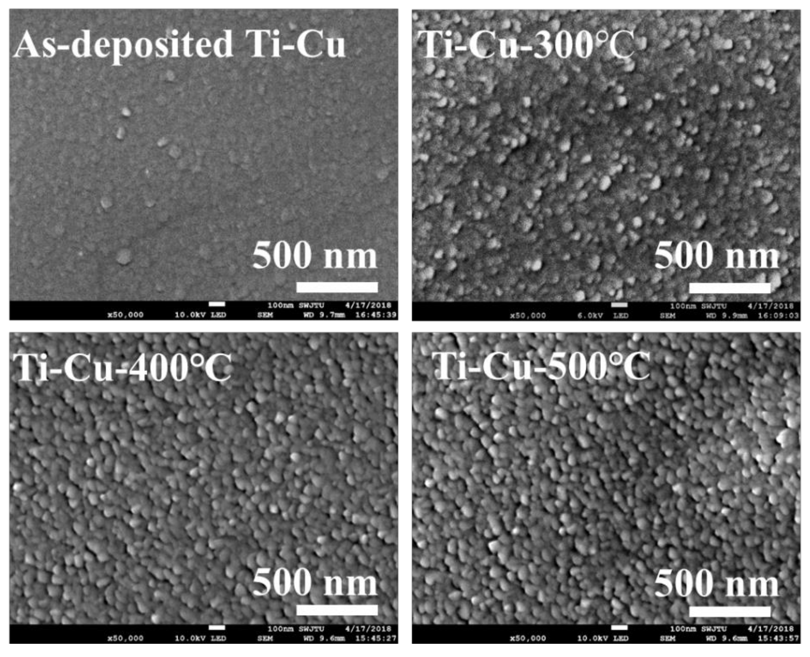
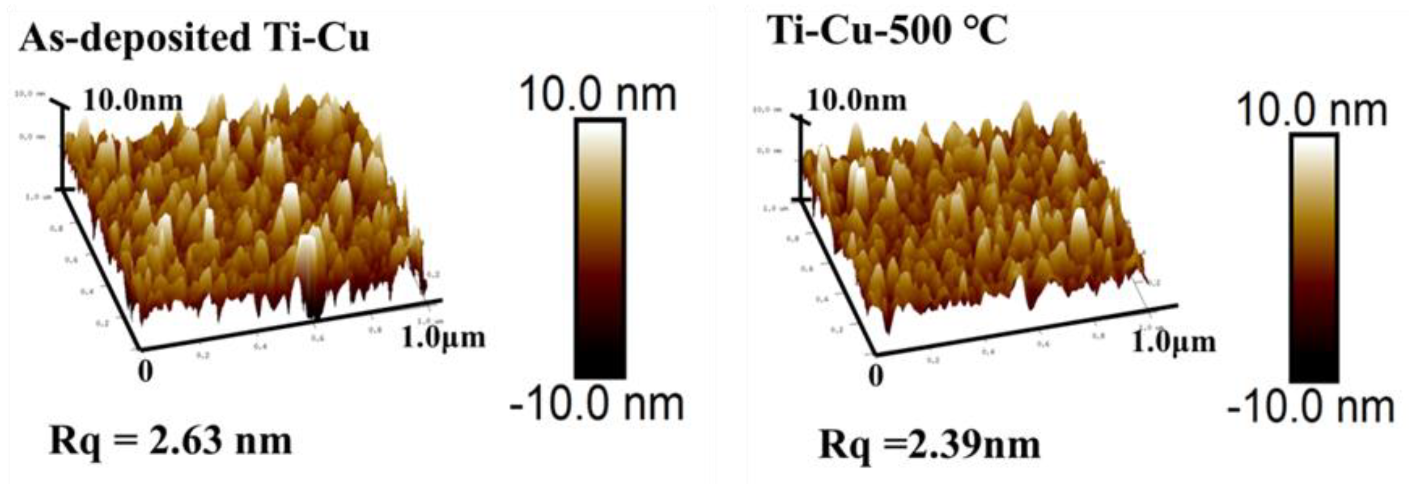
3.2. Surface Morphology

Figure 6 shows the SEM surface morphology of as-deposited and annealed Ti–Cu coatings prepared on Si substrates. All annealed Ti–Cu coatings show more obvious particles on their surfaces compared to as-deposited Ti–Cu coatings. Noncontiguous hillocks or islands are probably formed at 300 °C, and then grow up and form continuous hillocks or islands with clear boundaries after annealing at 400–500 °C. A similar phenomenon has been reported by Po Chen Lin, who found that annealing Cu (Ti) coatings with copper content of 62 at.% at 400 °C results in the formation of islands followed by their growth to form continuous Cu-rich layers [34]. Figure 7 shows the surface morphology and the corresponding root mean squared surface roughness (Rq) for the as-deposited and annealed Ti–Cu coatings deposited on Si substrates. The surface roughness of the Ti–Cu coatings annealed at 500 °C shows no significant change compared to the as-deposited coatings.

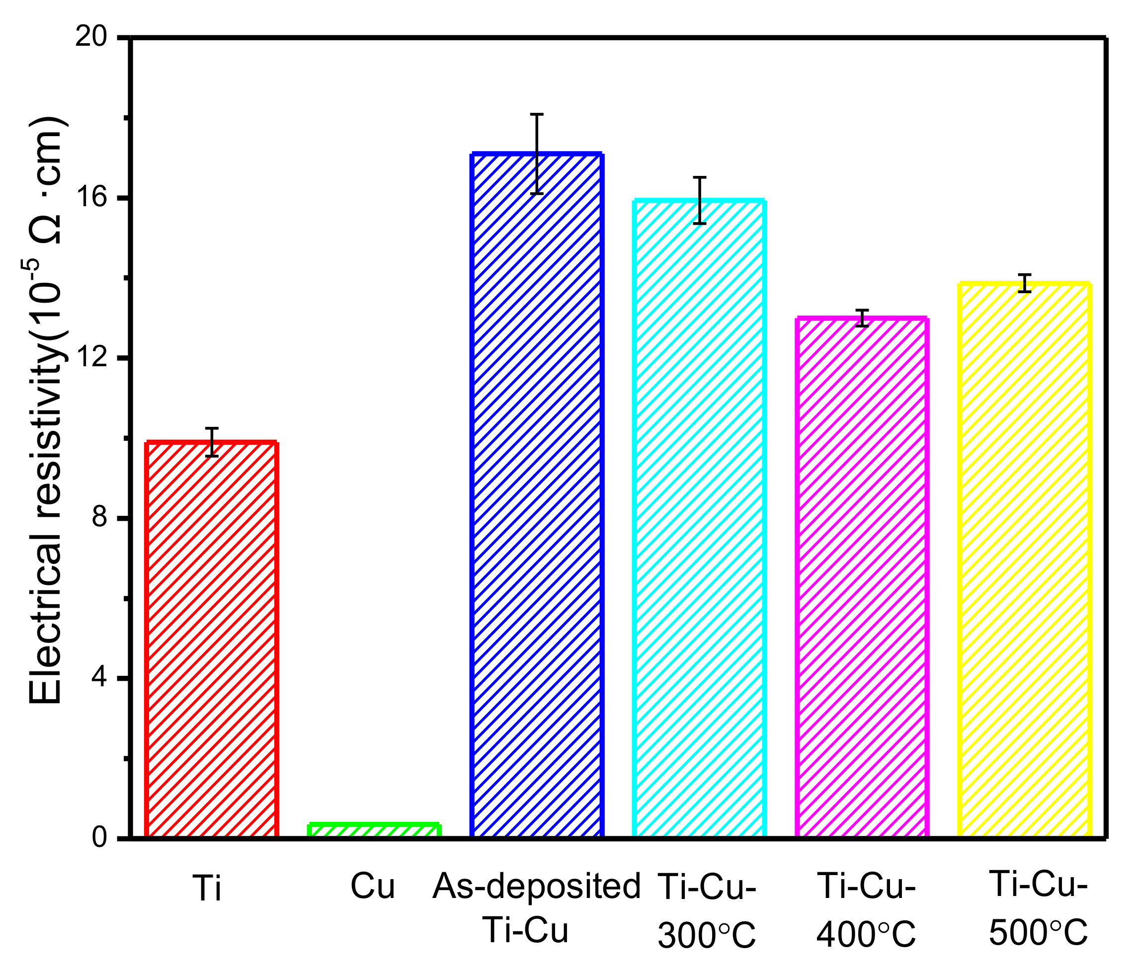
3.3. Electrical Resistivity of Ti–Cu Coatings

Annealing can affect the microstructure of the coatings, and thereby affecting the electrical resistivity that is critical for many applications including those in semiconductor industry or electroactive biomaterials [39,40]. The influence of vacuum annealing temperature on the electrical resistivity of the Ti–Cu coatings is studied using a four-probe device and the results are shown in Figure 8. The resistivity of the deposited Ti–Cu coatings (173.0 μΩ·cm) is higher than that of Ti coatings (99.0 μΩ·cm) and Cu coatings (3.6 μΩ·cm). Turnow et al. reported that the Ti–Cu coatings with Cu contents ranging from 10 to 78 at.% exhibit a higher resistivity (above 150 μΩ·cm) compared to pure Cu coatings [41]. The addition of Cu element makes it possible for Ti–Cu coatings to have a large number of non-equilibrium defects and metastable structure, thereby reducing the conductivity of free electrons and increasing the resistivity [41].
Figure 8 shows that the resistivity of Ti–Cu coatings annealed at 300–500 °C decreases compared with that of the deposited coatings. These results are in agreement with a study by Tsukimoto et al. showing that the resistivity of a Cu (Ti) alloy annealed at 400 °C decreases compared to that before annealing [25]. The EDS results (Figure 4f,g) showed that titanium diffuses to the surface and interface, while copper is enriched in the bulk of the coatings. It has been reported that the resistivity values of TiO compounds is 2.6 × 10⁻⁶ Ω·m [42], which is close to that of the as-deposited Ti–Cu coating. The formation of non-stoichiometric titanium oxides such as TiO or Ti3O is the main factor influencing the resistivity of the Ti–Cu coatings annealed at 500 °C. It has also been shown that the Ti atoms segregate on the surfaces and lead to a decrease in the resistivity for the Cu (Ti) coatings annealed at 400 °C [34]. Besides, the annealing process can reduce the non-equilibrium defects and metastable structure, resulting in the increase of the conductivity of free electrons and decrease of the resistivity [43,44]. It has been reported that the annealing process results in the reduction of resistivity for coatings such as sputter-deposited tungsten [45], Ga-doped ZnO [46], and Al–Ti-doped ZnO coatings [47]. Therefore, the decrease of resistivity is due to the uneven element distribution and decreased defects and metastable structures for the annealed Ti–Cu coating.

3.4. Electrochemical Corrosion of Ti–Cu Coatings

The electrochemical corrosion of the as-deposited and annealed Ti–Cu coatings on 316L SS substrates were evaluated using open-circuit potential and polarization curve test. Figure 9a shows the open-circuit potential for the as-deposited and annealed Ti–Cu samples. From a thermodynamic perspective, the more negative Ecorr value, the higher tendency for corrosion to occur [48]. The Ti–Cu coatings annealed at 300, 400, and 500 °C exhibit higher open-circuit potential than the as-deposited Ti–Cu coatings and 316L SS, indicating lower corrosion tendency. The coating annealed at 300 °C shows the lowest corrosion tendency.
Figure 9b shows the polarization curves of the 316L SS, deposited and annealed Ti–Cu coatings. Table 2 displays the self-corrosion potential (Ecorr) and self-corrosion current density (Icorr) of the samples according to the Tafel extrapolation method [49]. Similar to the open circuit potential, a higher Ecorr indicates a lower possibility of corrosion for these samples. In a previous study, it has been reported that the TiO2 coatings have greater Ecorr compared to Ti or SS substrates [50,51]. The presence of passivated metal oxides, as indicated by XPS and TEM results, may reduce the corrosion tendency of the annealed Ti–Cu coatings.
The corrosion rate of the coated samples is generally determined by the corrosion current density. Figure 9b and Table 2 show that all Ti–Cu coatings have lower corrosion current density compared with 316L SS, indicating lower corrosion rates. The Ti–Cu coating annealed at 300 °C show similar corrosion rate compared to the as-deposited Ti–Cu coating, while it increases for the Ti–Cu coatings annealed at 400 and 500 °C. These results correspond to the results of SEM surface morphology after polarization tests in Figure 9c. Figure 9c shows that 316L SS sample is severely corroded as evidenced by the appearance of deep and large pits. The deposited and annealed Ti–Cu coatings (300 °C) exhibit smooth surfaces without obvious pits, while the coatings annealed at 400 and 500 °C display shallow and small micro pits (1–3 μm in diameter).
Naka et al. found that the corrosion behavior of the amorphous Cu50Ti50 and Cu50Zr50 alloys is lower than that of the crystalline alloys with the same composition [52]. The reason is that the amorphous alloy has higher chemical uniformity and fewer crystal defects, such as precipitation, segregation, grain boundaries, and dislocations, forming a uniform and highly protective coating for passivation. The passivated metal oxides are formed after annealing according to the results of XPS and TEM. However, the TEM results (Figure 4) indicate that annealing can cause uneven element distribution for the Ti–Cu coatings. The XRD results (Figure 1) indicate crystal growth and crystallinity enhancement as increasing the annealing temperatures of Ti–Cu coatings. The uneven distribution of elements and improvements in crystallinity probably lead to increased corrosion behavior for the Ti–Cu coatings annealed at 400 and 500 °C.

3.5. Copper Ion Release of Ti–Cu Coatings

The copper ion release profile of Cu-bearing coatings can be affected by their Cu content [16], thickness [17], substrate roughness [53], and crystallographic structure [54]. The changes in Cu release profile are crucially important for biomedical applications as such changes significantly influence the function of the coatings such as their antibacterial activity and biocompatibility [15,16,55]. Figure 10a,b shows the concentration of released copper ions and release rate detected by ICP-MS after immersing in a PBS solution at 37 °C for 30 min, and 1–30 days for the as deposited and annealed Ti–Cu coatings. From Figure 10a, it is observed that the concentrations of the released copper ions are less for all the annealed Ti–Cu coatings compared with those released from the as-deposited coatings. The stable release of copper ions in PBS solution is within 0.8–1.0 μM for up to 30 days for all the annealed Ti–Cu coatings. A study by Ding et al. concluded that greater release rates of copper ions in natural seawater occur for Cu/Cu2O coatings with higher Cu2O contents [54]. TEM and corresponding EDS results show that the Cu element is enriched in the bulk of the annealed coatings, possibly resulting in the inhibition of the copper ion release compared to as-deposited coatings. Figure 10b shows that the release rate of all samples in the first 30 min is high, indicating the burst release of copper ions. After the initial decline, all the release rates remain almost stable ranging from 0.008 to 0.003 μmol/cm2·d·L for immersing time of up to 30 days. These results suggest that vacuum annealing affects the Cu diffusion of Ti–Cu coatings, and thereby affecting the copper ion releasing profiles.

4. Conclusions

Ti–Cu coatings were fabricated using HPPMS/DC magnetron co-sputtering followed by vacuum annealing at temperatures of 300, 400, and 500 °C. XRD and cross-sectional TEM results showed that as-deposited Ti–Cu coatings mainly contain nanocrystals such as Ti, Cu, and CuTi3, while Ti3O/TiO, Cu2O, and CuTi3 nanocrystals are mainly present in the annealed coatings. TEM results also showed that Ti and Cu elements are uniformly distributed in the deposited Ti–Cu coatings, while Cu is enriched in the bulk of the coatings and Ti diffuses to the surface and interfaces between the coatings and the silicon substrates for the coating annealed at 500 °C. XPS results before and after Ar ion etching provided evidence that TiO2, Cu2O, and CuO are present on the surfaces, while Cu2O, TiO2, Ti2O3, and TiO are formed in the bulk of the coatings annealed at 500 °C. SEM results demonstrated that the surfaces of annealed Ti–Cu coatings have more obvious particles than that of the deposited Ti–Cu coatings. Both as-deposited and annealed Ti–Cu coatings show higher resistivity than Ti and Cu coatings. The resistivity of Ti–Cu coatings annealed at 300–500 °C decreases compared with that of the deposited coatings. The uneven elemental distribution and improvement of crystallinity decrease the electrical resistivity of the annealed Ti–Cu coatings. The corrosion behavior of the Ti–Cu coatings annealed at 300 °C is similar to that of the deposited Ti–Cu coatings, while it increases for the Ti–Cu coatings annealed at 400 and 500 °C. The concentration of released copper ions of Ti–Cu coatings annealed at 300, 400, and 500 °C slightly decreases compared with that of as-deposited coatings. The release rates remain almost unchanged in the range of 0.008 to 0.003 μmol/cm2·d·L for immersion times of up to 30 days. We have demonstrated that vacuum annealing affects the Cu diffusion and microstructure of Ti–Cu coatings, and thereby affects the resistivity, corrosion properties, and copper ion releasing behaviors.

Author Contributions

Conceptualization, F.J.; methodology, L.Q., F.J., and B.A.; formal analysis, L.Q., B.H., and B.A.; investigation, L.Q. and B.H.; resources, P.J. and Y.L. (Yantao Li); writing—original draft preparation, L.Q. and D.M.; writing—review and editing, D.M., D.X., F.J., and B.A.; supervision, F.J.; project administration, F.J. and Y.L. (Yongxiang Leng), and N.H.; funding acquisition, F.J. All authors have read and agreed to the published version this manuscript.

Funding

This research was funded by National Nature Science Foundation of China, Grant No. 31300787 and Nature Science Associate Foundation, Grant No. U1330113.

Acknowledgments

This work was supported by NSFC (No. 31300787) and NSAF (Grant No. U1330113), and the technical support of the unbalanced magnetron sputtering (UBMS450) of Southwest Jiaotong University was acknowledged.

Conflicts of Interest

The authors declare no conflict of interest.

References

  1. Kaur, M.; Singh, K. Review on titanium and titanium based alloys as biomaterials for orthopaedic applications. Mater. Sci. Eng. C 2019, 102, 844–862. [Google Scholar] [CrossRef] [PubMed]
  2. Mohammed, M.T.; Khan, Z.A.; Siddiquee, A.N. Surface Modifications of Titanium Materials for developing Corrosion Behavior in Human Body Environment: A Review. Procedia Mater. Sci. 2014, 6, 1610–1618. [Google Scholar] [CrossRef] [Green Version]
  3. Chu, C.; Wang, R.M.; Hu, T.; Yin, L.H.; Pu, Y.P.; Lin, P.H.; Dong, Y.S.; Guo, C.; Chung, C.; Yeung, K.W.K.; et al. XPS and biocompatibility studies of titania film on anodized NiTi shape memory alloy. J. Mater. Sci. Mater. Electron. 2008, 20, 223–228. [Google Scholar] [CrossRef] [PubMed]
  4. Rezaee, S.; Arman, A.; Jurečka, S.; Korpi, A.G.; Mwema, F.; Luna, C.; Sobola, D.; Kulesza, S.; Shakoury, R.; Bramowicz, M.; et al. Effect of annealing on the micromorphology and corrosion properties of Ti/SS thin films. Superlattices Microstruct. 2020, 146, 106681. [Google Scholar] [CrossRef]
  5. Williamson, M.A. Geochemistry; Springer: Dordrecht, The Netherlands, 1998; pp. 101–102. [Google Scholar]
  6. Michels, H.; Noyce, J.; Keevil, C.W. Effects of temperature and humidity on the efficacy of methicillin-resistant Staphylococcus aureus challenged antimicrobial materials containing silver and copper. Lett. Appl. Microbiol. 2009, 49, 191–195. [Google Scholar] [CrossRef] [Green Version]
  7. Domanskaya, I.K.; Tropnikov, D.L. Prospects of Application of Waste Copper Slags as Fillers for Building Materials. Tsvetnye Met. 2014. Available online: http://www.rudmet.com/journal/1347/article/23061/ (accessed on 1 October 2020).
  8. Natter, H.; Schmelzer, M.; Hempelmann, R. Nanocrystalline nickel and nickel-copper alloys: Synthesis, characterization, and thermal stability. J. Mater. Res. 1998, 13, 1186–1197. [Google Scholar] [CrossRef]
  9. Duwez, P.; Willens, R.H.; Klement, W. Continuous Series of Metastable Solid Solutions in Silver-Copper Alloys. J. Appl. Phys. 1960, 31, 1136. [Google Scholar] [CrossRef]
  10. Bacon, G.E.; Dunmur, I.W.; Smith, J.H.; Street, R. The antiferromagnetism of manganese copper alloys. Proc. R. Soc. London Ser. A Math. Phys. Sci. 1957, 241, 223–238. [Google Scholar] [CrossRef]
  11. Lopes, C.; Vieira, M.; Borges, J.; Fernandes, J.; Rodrigues, M.; Alves, E.; Barradas, N.; Apreutesei, M.; Steyer, P.; Tavares, C.; et al. Multifunctional Ti–Me (Me=Al, Cu) thin film systems for biomedical sensing devices. Vacuum 2015, 122, 353–359. [Google Scholar] [CrossRef]
  12. Lin, Q.-J.; Yang, S.; Wang, C.-Y.; Ding, J.-J.; Jiang, Z.-D. Multifractal analysis for Cu/Ti bilayer thin films. Surf. Interface Anal. 2013, 45, 1223–1227. [Google Scholar] [CrossRef]
  13. Swain, M.; Bhattacharya, D.; Basu, S. Deposition of optical quality Cu/Ti films. In Proceedings of the 58th DAE Solid State Physics Symposium 2013, Punjab, India, 17–21 December 2013. [Google Scholar]
  14. Jin, X.; Gao, L.; Liu, E.; Yu, F.; Shu, X.; Wang, H. Microstructure, corrosion and tribological and antibacterial properties of Ti–Cu coated stainless steel. J. Mech. Behav. Biomed. Mater. 2015, 50, 23–32. [Google Scholar] [CrossRef] [Green Version]
  15. Stranak, V.; Wulff, H.; Rebl, H.; Zietz, C.; Arndt, K.; Bogdanowicz, R.; Nebe, B.; Bader, R.; Podbielski, A.; Hubička, Z.; et al. Deposition of thin titanium–copper films with antimicrobial effect by advanced magnetron sputtering methods. Mater. Sci. Eng. C 2011, 31, 1512–1519. [Google Scholar] [CrossRef]
  16. Huang, B.; Jing, F.; Akhavan, B.; Ji, L.; Leng, Y.; Xie, D.; Bilek, M.; Huang, N. Multifunctional Ti-xCu coatings for cardiovascular interfaces: Control of microstructure and surface chemistry. Mater. Sci. Eng. C 2019, 104, 109969. [Google Scholar] [CrossRef]
  17. Wang, Q.; Akhavan, B.; Jing, F.; Cheng, D.; Sun, H.; Xie, N.; Leng, Y.; Bilek, M.M.; Huang, N. Catalytic Formation of Nitric Oxide Mediated by Ti–Cu Coatings Provides Multifunctional Interfaces for Cardiovascular Applications. Adv. Mater. Interfaces 2018, 5, 1701487. [Google Scholar] [CrossRef]
  18. Horton, D.; Ha, H.; Foster, L.L.; Bindig, H.; Scully, J. Tarnishing and Cu Ion release in Selected Copper-Base Alloys: Implications towards Antimicrobial Functionality. Electrochim. Acta 2015, 169, 351–366. [Google Scholar] [CrossRef]
  19. Qiao, Y.; Ping, Y.; Zhang, H.; Zhou, B.; Liu, F.; Yu, Y. Laser-activatable CuS nanodots to treat multidrug-resistant bacteria and release copper ion to accelerate healing of Iinfected chronic nonhealing wounds. ACS Appl. Mater. Interfaces 2019, 11, 3809–3822. [Google Scholar] [CrossRef] [Green Version]
  20. Gritsch, L.; Lovell, C.; Goldmann, W.H.; Boccaccini, A.R. Fabrication and characterization of copper(II)-chitosan complexes as antibiotic-free antibacterial biomaterial. Carbohydr. Polym. 2018, 179, 370–378. [Google Scholar] [CrossRef]
  21. Foley, J.; Blackwell, A. Ion Release from Copper Phosphate Cement and Influence on Streptococcus mutans Growth in vitro: A Comparative Study. Caries Res. 2003, 37, 416–424. [Google Scholar] [CrossRef]
  22. Christensen, G.D.; Baldassarri, L.; Simpson, W.A. Methods for studying microbial colonization of plastics. Methods Enzymol. 1995, 253, 477–500. [Google Scholar] [CrossRef]
  23. Chen, W.; Meng, X.; Wu, D.; Yao, D.; Zhang, D. The effect of vacuum annealing on microstructure, adhesion strength and electrochemical behaviors of multilayered AlCrTiSiN coatings. Appl. Surf. Sci. 2019, 468, 391–401. [Google Scholar] [CrossRef]
  24. Yang, J.; Xiao, S.; Zhang, Q.; Xu, C.; Li, W.; Zheng, B.; Hu, F.; Yin, J.; Song, Z. In-situ synthesis of Ti–Al intermetallic compounds coating on Ti alloy by magnetron sputtering deposition followed by vacuum annealing. Vacuum 2020, 172, 109060. [Google Scholar] [CrossRef]
  25. Tsukimoto, S.; Morita, T.; Moriyama, M.; Ito, K.; Murakami, M. Formation of Ti diffusion barrier layers in Thin Cu(Ti) alloy films. J. Electron. Mater. 2005, 34, 592–599. [Google Scholar] [CrossRef]
  26. Sarakinos, K.; Alami, J.; Konstantinidis, S. High power pulsed magnetron sputtering: A review on scientific and engineering state of the art. Surf. Coat. Technol. 2010, 204, 1661–1684. [Google Scholar] [CrossRef]
  27. Najafi-Ashtiani, H.; Akhavan, B.; Jing, F.; Bilek, M.M.M. Transparent Conductive Dielectric–Metal–Dielectric Structures for Electrochromic Applications Fabricated by High-Power Impulse Magnetron Sputtering. ACS Appl. Mater. Interfaces 2019, 11, 14871–14881. [Google Scholar] [CrossRef]
  28. Ganesan, R.; Akhavan, B.; Partridge, J.G.; McCulloch, D.G.; McKenzie, D.R.; Bilek, M.M.M. Evolution of target condition in reactive HiPIMS as a function of duty cycle: An opportunity for refractive index grading. J. Appl. Phys. 2017, 121, 171909. [Google Scholar] [CrossRef]
  29. Akhavan, B.; Ganesan, R.; Stueber, M.; Ulrich, S.; McKenzie, D.R.; Bilek, M.M.M. Carbon films deposited by mixed-mode high power impulse magnetron sputtering for high wear resistance: The role of argon incorporation. Thin Solid Film. 2019, 688, 137353. [Google Scholar] [CrossRef]
  30. Ganesan, R.; Akhavan, B.; Hiob, M.A.; McKenzie, D.R.; Weiss, A.S.; Bilek, M.M. HiPIMS carbon coatings show covalent protein binding that imparts enhanced hemocompatibility. Carbon 2018, 139, 118–128. [Google Scholar] [CrossRef]
  31. Gorzalski, A.S.; Donley, C.; Coronell, O. Elemental composition of membrane foulant layers using EDS, XPS, and RBS. J. Membr. Sci. 2017, 522, 31–44. [Google Scholar] [CrossRef] [Green Version]
  32. Lau, K.; Akhavan, B.; Lord, M.S.; Bilek, M.M.; Rnjak-Kovacina, J. Dry Surface Treatments of Silk Biomaterials and Their Utility in Biomedical Applications. ACS Biomater. Sci. Eng. 2020, 6, 5431–5452. [Google Scholar] [CrossRef]
  33. Miler, M.; Mirtič, B. Accuracy and precision of EDS analysis for identification of metal-bearing minerals in polished and rough particle samples. Geologija 2013, 56, 5–17. [Google Scholar] [CrossRef]
  34. Lin, P.C.; Chen, H.; Hsieh, H.-C.; Tseng, T.-H.; Lee, H.Y.; Wu, A.T. Co-sputtered Cu(Ti) thin alloy film for formation of Cu diffusion and chip-level bonding. Mater. Chem. Phys. 2018, 211, 17–22. [Google Scholar] [CrossRef]
  35. Gouttebaron, R.; Cornelissen, D.; Snyders, R.; Dauchot, J.P.; Wautelet, M.; Hecq, M. XPS study of TiOx thin films prepared by d.c. magnetron sputtering in Ar–O2 gas mixtures. Surf. Interface Anal. 2015, 30, 527–530. [Google Scholar] [CrossRef]
  36. Hashimoto, S.; Tanaka, A.; Murata, A.; Sakurada, T. Formulation for XPS spectral change of oxides by ion bombardment as a function of sputtering time. Surf. Sci. 2004, 556, 22–32. [Google Scholar] [CrossRef]
  37. Cano, E.; Tôrres, C.L.; Bastidas, J.M. An XPS study of copper corrosion originated by formic acid vapour at 40% and 80% relative humidity. Mater. Corros. 2001, 52, 667–676. [Google Scholar] [CrossRef]
  38. Poulston, S.; Parlett, P.M.; Stone, P.; Bowker, M. Surface oxidation and reduction of CuO and Cu2O studied using XPS and XAES. Surf. Interface Anal. 1996, 24, 811–820. [Google Scholar] [CrossRef]
  39. Luo, B.; Li, K.; Tan, X.; Zhang, J.; Luo, J.; Jiang, X.; Wu, W.; Tang, Y. Influences of in situ annealing on microstructure, residual stress and electrical resistivity for sputter-deposited Be coating. J. Alloys Compd. 2014, 607, 150–156. [Google Scholar] [CrossRef]
  40. Li, W.Y.; Li, C.-J.; Liao, H. Effect of Annealing Treatment on the Microstructure and Properties of Cold-Sprayed Cu Coating. J. Therm. Spray Technol. 2006, 15, 206–211. [Google Scholar] [CrossRef]
  41. Turnow, H.; Wendrock, H.; Menzel, S.B.; Gemming, T.; Eckert, J. Structure and properties of sputter deposited crystalline and amorphous Cu–Ti films. Thin Solid Films 2016, 598, 184–188. [Google Scholar] [CrossRef]
  42. Cacucci, A.; Tsiaoussis, I.; Potin, V.; Imhoff, L.; Martin, N.; Nyberg, T. The interdependence of structural and electrical properties in TiO2/TiO/Ti periodic multilayers. Acta Mater. 2013, 61, 4215–4225. [Google Scholar] [CrossRef] [Green Version]
  43. Ben Saâd, H.; Ajili, M.; Dabbebi, S.; Kamoun, N.T. Investigation on thickness and annealing effects on physical properties and electrical circuit model of CuO sprayed thin films. Superlattices Microstruct. 2020, 142, 106508. [Google Scholar] [CrossRef]
  44. Wen, Y.; Yunxin, W.; Hai, G. Molecular dynamics simulations of the effects of annealing on the micro residual stress induced by vacancy defects in aluminum crystal. J. Cryst. Growth 2020, 546, 125754. [Google Scholar] [CrossRef]
  45. Choi, D.; Wang, B.; Chung, S.; Liu, X.; Darbal, A.; Wise, A.; Nuhfer, N.T.; Barmak, K.; Warren, A.P.; Coffey, K.R.; et al. Phase, grain structure, stress, and resistivity of sputter-deposited tungsten films. J. Vac. Sci. Technol. A 2011, 29, 051512. [Google Scholar] [CrossRef] [Green Version]
  46. Sheu, J.-K.; Shu, K.W.; Lee, M.L.; Tun, C.J.; Chi, G.C. Effect of Thermal Annealing on Ga-Doped ZnO Films Prepared by Magnetron Sputtering. J. Electrochem. Soc. 2007, 154, H521. [Google Scholar] [CrossRef]
  47. Minhong, J.; Liu, X. Structural, electrical and optical properties of Al–Ti codoped ZnO (ZATO) thin films prepared by RF magnetron sputtering. Appl. Surf. Sci. 2008, 255, 3175–3178. [Google Scholar] [CrossRef]
  48. Kotyk, J.F.K.; Chen, C.; Sheehan, S.W. Corrosion Potential Modulation on Lead Anodes Using Water Oxidation Catalyst Coatings. Coatings 2018, 8, 246. [Google Scholar] [CrossRef] [Green Version]
  49. Yang, H.; Guo, X.; Wu, G.; Wang, S.; Ding, W. Continuous intermetallic compounds coatings on AZ91D Mg alloy fabricated by diffusion reaction of Mg–Al couples. Surf. Coat. Technol. 2011, 205, 2907–2913. [Google Scholar] [CrossRef]
  50. Ren, Q.; Qin, L.; Jing, F.; Cheng, D.; Wang, Y.; Yang, M.; Xie, D.; Leng, Y.; Akhavan, B.; Huang, N. Reactive magnetron co-sputtering of Ti-xCuO coatings: Multifunctional interfaces for blood-contacting devices. Mater. Sci. Eng. C 2020, 116, 111198. [Google Scholar] [CrossRef] [PubMed]
  51. Wang, Q.; Zhang, P.-Z.; Wei, D.; Wang, R.-N.; Chen, X.-H.; Wang, H.-Y. Microstructure and corrosion resistance of pure titanium surface modified by double-glow plasma surface alloying. Mater. Des. 2013, 49, 1042–1047. [Google Scholar] [CrossRef]
  52. Naka, M.; Hashimoto, K.; Masumoto, T. Corrosion behavior of amorphous and crystalline Cu50Ti50 and Cu50Zr50 alloys. J. Non-Cryst. Solids 1978, 30, 29–36. [Google Scholar] [CrossRef]
  53. Zietz, C.; Fritsche, A.; Finke, B.; Stranak, V.; Haenle, M.; Hippler, R.; Mittelmeier, W.; Bader, R. Analysis of the Release Characteristics of Cu-Treated Antimicrobial Implant Surfaces Using Atomic Absorption Spectrometry. Bioinorg. Chem. Appl. 2011, 2012, 32. [Google Scholar] [CrossRef]
  54. Ding, R.; Li, X.; Wang, J.; Li, W.; Wang, X.; Gui, T. Antifouling Properties and Release of Dissolved Copper of Cold Spray Cu/Cu2O Coatings for Ships and Steel Structures in Marine Environment. J. Mater. Eng. Perform. 2018, 27, 5947–5963. [Google Scholar] [CrossRef]
  55. Finke, B.; Polak, M.; Hempel, F.; Rebl, H.; Zietz, C.; Stranak, V.; Lukowski, G.; Hippler, R.; Bader, R.; Nebe, J.B.; et al. Antimicrobial Potential of Copper-Containing Titanium Surfaces Generated by Ion Implantation and Dual High Power Impulse Magnetron Sputtering. Adv. Eng. Mater. 2011, 14, B224–B230. [Google Scholar] [CrossRef]
Figure 1. (a,d,g,j) Surface morphology evaluated by SEM, (b,e,h,k) the distribution of Cu and Ti elements evaluated by energy dispersive X-ray spectroscopy (EDS) mapping corresponded to SEM images, and (c,f,i,l) the EDS spectra corresponded to SEM images for the Ti–Cu coatings deposited on silicon substrates. The images are obtained from samples before (as-deposited) and after annealing at various temperatures of 300, 400, and 500 °C (red points for Ti, and green points for Cu for the EDS mapping).
Coatings 10 01064 g001
Figure 2. X-ray diffraction (XRD) patterns of Ti, Cu, and Ti–Cu coatings deposited on silicon substrates before and after annealing at temperatures of 300 °C, 400 °C, and 500 °C.
Coatings 10 01064 g002
Figure 3. Cross-sectional transmission electron microscopy (TEM) results obtained for the as-deposited Ti–Cu coatings on silicon substrates: (a) low magnification field image; (b) selective area electron diffraction (SAED) image; (c,d) high-resolution transmission electron microscopy (HRTEM) images; (e) EDS line scans showing the distributions of elements (Pt, Ti, Si, Cu, O) in the high-angle annular dark-field (HADDF) image; (f) corresponding EDS mappings showing the distribution of elements (Pt, Ti, Si, Cu) in the HADDF image.
Coatings 10 01064 g003
Figure 4. Cross-sectional transmission electron microscopy (TEM) results obtained for the Ti–Cu coatings annealed at the temperature of 500 °C on silicon substrates: (a) low magnification field image; (b,c) corresponding HRTEM images; (d) corresponding selective area electron diffraction (SAED) image; (e) corresponding HRTEM images; (f) EDS line scans showing the distributions of the elements (Pt, Ti, Si, Cu, O) in the high-angle annular dark-field (HADDF) image; (g) corresponding EDS mappings of the distribution of elements (Pt, Ti, Si, Cu) in the HADDF image.
Coatings 10 01064 g004
Figure 5. (ad) Ti2p peak fitted spectra of the Ti–Cu coatings deposited on silicon substrates and annealed at 500 °C before (etching for 0 s) and after Ar+ ion etching for 20, 60, and 180 s; (e) relative area (%) of Ti (IV), Ti (III), Ti (II)) in Ti2p spectra of the Ti–Cu coatings annealed at 500 °C before and after etching; (fi) Cu2p Peak fitted spectra of the Ti–Cu coatings deposited on silicon substrates and annealed at 500 °C before (etching for 0 s) and after Ar+ ion etching for 20, 60, and 180 s; (j) relative area (%) of Cu(II) and Cu(I) in Cu2p spectra of the Ti–Cu coatings annealed at 500 °C before and after etching.
Coatings 10 01064 g005
Figure 6. SEM micrographs showing the surface morphologies of Ti–Cu coatings before (as-deposited) and after annealing at varied temperature of 300, 400, and 500 °C. The coatings were deposited on silicon substrates.
Coatings 10 01064 g006
Figure 7. Surface morphology and corresponding root mean squared surface roughness (Rq) evaluated by AFM for the Ti–Cu coatings before (as-deposited) and after annealing at 500 °C (Ti–Cu- 500 °C). The coatings were deposited on silicon substrates.
Coatings 10 01064 g007
Figure 8. Resistivity of Ti, Cu, as-deposited Ti–Cu, and Ti–Cu coatings annealed at varied temperatures of 300 °C, 400 °C, and 500 °C on silicon substrates.
Coatings 10 01064 g008
Figure 9. (a) Open circuit potential and (b) polarization curves of the deposited and annealed Ti–Cu coatings (300 °C, 400 °C, and 500 °C) deposited on 316L SS substrates; (c) Surface morphologies evaluated by SEM images after electrochemical corrosion for the deposited and annealed Ti–Cu coatings on 316L SS substrates.
Coatings 10 01064 g009
Figure 10. (a) The accumulated Cu ions and (b) release rate of Cu ions of the deposited and annealed Ti–Cu coatings (300 °C, 400 °C, 500 °C) deposited on silicon substrates after immersion in PBS solution (pH = 7.4) for durations from 30 min to 30 days.
Coatings 10 01064 g010
Table 1. Cu contents evaluated by EDS for the deposited and annealed Ti–Cu coatings.
SamplesAs–Deposited Ti-CuTi–Cu-300 °CTi–Cu-400 °CTi–Cu-500 °C
Cu/(Cu + Ti) values (at.%)12.114.919.515.4
Table 2. The corrosion potential (Ecorr) and current densities (Icorr) of 316L SS and Ti–Cu coatings before and after annealing at 300 °C, 400 °C, and 500 °C.
SampleEcorr (V)Icorr (A·cm−2)
316L SS−0.3753.38 × 10−7
As-deposited Ti-Cu−0.2931.07 × 10−8
Ti-Cu-300 °C0.0041.42 × 10−8
Ti-Cu-400 °C−0.0261.24 × 10−7
Ti-Cu-500 °C−0.0161.76 × 10−7
Publisher’s Note: MDPI stays neutral with regard to jurisdictional claims in published maps and institutional affiliations.

