Review

Functionalization of 2D MoS2 Nanosheets with Various Metal and Metal Oxide Nanostructures: Their Properties and Application in Electrochemical Sensors

by
Ntsoaki Mphuthi
1,2,
Lucky Sikhwivhilu
1,3,* and
Suprakas Sinha Ray
2,4,*
1
DSI-Mintek Nanotechnology Innovation Centre, Randburg 2125, South Africa
2
Department of Chemical Sciences, University of Johannesburg, Doornfontein 2028, South Africa
3
Department of Chemistry, Faculty of Science, Engineering and Agriculture, University of Venda, Private Bag X5050, Thohoyandou 0950, South Africa
4
Centre for Nanostructures and Advanced Materials, DSI-CSIR Nanotechnology Innovation Centre, Council for Scientific Industrial Research, Pretoria 0001, South Africa
*
Authors to whom correspondence should be addressed.
Biosensors 2022, 12(6), 386; https://doi.org/10.3390/bios12060386
Submission received: 29 April 2022 / Revised: 25 May 2022 / Accepted: 29 May 2022 / Published: 2 June 2022
(This article belongs to the Section Biosensor Materials)

Abstract

:
Two-dimensional transition metal dichalcogenides (2D TMDs) have gained considerable attention due to their distinctive properties and broad range of possible applications. One of the most widely studied transition metal dichalcogenides is molybdenum disulfide (MoS2). The 2D MoS2 nanosheets have unique and complementary properties to those of graphene, rendering them ideal electrode materials that could potentially lead to significant benefits in many electrochemical applications. These properties include tunable bandgaps, large surface areas, relatively high electron mobilities, and good optical and catalytic characteristics. Although the use of 2D MoS2 nanosheets offers several advantages and excellent properties, surface functionalization of 2D MoS2 is a potential route for further enhancing their properties and adding extra functionalities to the surface of the fabricated sensor. The functionalization of the material with various metal and metal oxide nanostructures has a significant impact on its overall electrochemical performance, improving various sensing parameters, such as selectivity, sensitivity, and stability. In this review, different methods of preparing 2D-layered MoS2 nanomaterials, followed by different surface functionalization methods of these nanomaterials, are explored and discussed. Finally, the structure–properties relationship and electrochemical sensor applications over the last ten years are discussed. Emphasis is placed on the performance of 2D MoS2 with respect to the performance of electrochemical sensors, thereby giving new insights into this unique material and providing a foundation for researchers of different disciplines who are interested in advancing the development of MoS2-based sensors.

1. Introduction

Layered materials have been studied for several years. Each layered material, when thinned to its physical limit, reveals novel properties different from its bulk counterpart. Therefore, at the physical limit, these materials are referred to as two-dimensional (2D) materials [1]. These 2D materials have received great attention due to the affluence of unusual physical characteristics that occur when charge and heat transports are confined to a plane [2]. Graphene is the most widely studied 2D material because of its exceptional properties. It is composed of a single layer of carbon atoms arranged in a 2D honeycomb lattice [3]. It is a fundamental building block for a range of well-known carbon materials such as three-dimensional (3D) graphite, one-dimensional (1D) carbon nanotubes, and zero-dimensional (0D) fullerene [3]. Since its isolation, it has inspired thoughtful research on other 2D materials. These materials are useful building blocks that can be restacked and incorporated into composites for a wide range of applications. Other than graphene, recent efforts have focused on other 2D materials (ranging from conductors to insulators). These materials include transition metal dichalcogenides (TMDs) as semiconductors involving a general chemical formula of MX2, where M is a transition metal atom (M = Mo, W, Ti, Zr, Ta, Nb, Re, Ni, or V) and X is a chalcogenides atom (X = S, Se, Te), as well as black phosphorus (BP), transition metal oxides, and hexagonal boron nitride (hBN) as an insulator [3,4,5]. TMDs are now the key focus of many researchers because of their unique properties. Exfoliated 2D TMDs have properties that are complementary to (but yet distinct from) those of graphene, and they also have the advantages of tunable bandgaps ranging from 1–2 eV [4,6,7]. One of the most widely explored transition metal dichalcogenides is molybdenum disulfide (MoS2) [8,9,10]. The electrical and optical properties of MoS2 are layer-dependent. For instance, bulk MoS2 is an n-type semiconductor with an indirect bandgap of about 1.3 eV, while a monolayer MoS2 has a direct bandgap of 1.8 eV [6,11]. Moreover, monolayer MoS2 exhibits carrier mobility of 200 cm2V−1s−1 at room temperature with a high on/off current ratio of ~108 [12]. MoS2 has a layered crystal structure formed by stacking covalently bound S-Mo-S monolayers through weak van der Waals interactions [13,14]. The van der Waals interlayer interaction between these monolayers allows for their separation leading to crystal exfoliation with approximately 0.65 nm of thickness (6.5 Å) [12,15].
As a semiconducting analog of graphene, this material has recently been reported as promising in the application of sensors [13], photodetectors [16], transistors [12], flexible electronics [17], and fuel cells [18]. Although the use of MoS2 nanosheets offers many advantages, poor conductivity (due to the large bandgaps) considerably limits their practical applications in sensors. Moreover, it has been reported that pristine MoS2 nanosheets suffer from gradual degradation at ambient conditions, which are triggered by surface contamination and significant adsorption of oxygen in an air environment. This leads to instability and decreased electrical properties and sensing abilities [19,20]. Therefore, to obtain satisfactory results, pristine MoS2 nanosheets need to be operated in an inert atmosphere. To overcome these limitations and extend the potential application of MoS2 nanosheets, various approaches have been attempted, such as the substitution of the transition metal of MoS2 with other elements [21], molecular physisorption of organic materials [22], changing interfacial chemistry [23,24], solution-based chemical doping [25], and promoting structural phase transition (from semiconducting 2H phase to metallic 1T phase) [26,27]. However, some of these methods are complicated and time-consuming; some result in structural defects, reduced mobility, and unstable composites [28]. Furthermore, researchers noted that TMDs have a habit of being inert to chemical functionalization. Chalcogen atoms in the basal plane of TMD nanosheets are saturated and, therefore, are not highly reactive, whereas the metal sites in TMDs are embedded beneath the chalcogen layer, all but eliminating them from being useful for functionalization [29]. Despite this, it is necessary to functionalize MoS2 with chemical moieties, which can enable its interface with other nano- or micro-structures [15]. The synergetic effects resulting from MoS2 composites can produce enhanced properties or improved performances. The large surface-to-volume ratio of 2D MoS2 nanosheets presents an opportunity for the effective surface functionalization of the material with metal and metal oxide nanostructures (NSs). Compared with previously described methods of functionalization, interfacing 2D MoS2 nanosheets with metal-based NSs is more simply carried out and offers an additional path for controlling the thermal, catalytic, magnetic, optical, and electrical properties. Based on theoretical calculations, it has been reported that the effective adsorption of different metal atoms on 2D MoS2 is related to the number of d -electrons, which can also effectively modulate the band structures of the material [30]. Most metal-based NSs have good stability and are resistant to environmental deterioration and oxidation, which make them ideal for the fabrication of nanocomposites. However, it is worth noting that the structures and properties of nanocomposites are dependent on the conditions of the composite synthesis and the control of the decorated location, morphology, and number density of the NSs [31]. Recently, metal and metal oxide nanocomposites have received a great deal of attention because of their excellent physical and chemical properties, which expanded their application in sensors [20,31], electrocatalysis [32,33], and optoelectronics [34]. Thus, it can be expected that 2D MoS2 nanosheets decorated with metal-based NSs could potentially extend their applications as novel nanomaterials in sensors. For instance, 2D MoS2 functionalized with metal and metal oxide NSs, such as nickel (Ni) [35], gold (Au) [36], and tricobalt tetraoxide (Co3O4) [37], to name a few, was reported to exhibit excellent catalytic sensing properties. The MoS2-Ni nanocomposite demonstrated good reproducibility and excellent sensitivity toward glucose detection. The reported results showed that small Ni nanoparticles (NPs) on the surface of the MoS2 nanosheet had more active sites, resulting in high electrocatalytic activity and a fast response time of less than 2 s. In addition, it was discovered that Ni NPs without MoS2 support appeared to aggregate, which was detrimental to the electrocatalytic activity of the sensor [35]. The MoS2-Co3O4 nanocomposites showed high sensitivity and fast response and recovery features for the detection of ammonia at room temperature. The sensing film was constructed on an interdigital electrode substrate using layer-by-layer self-assembly of MoS2 nanosheets and Co3O4 nanorods. The layer-by-layer self-assembly not only efficiently prevented agglomeration but also provided many more active catalytic sites on p-type Co3O4 nanorods toward ammonia. The results indicated that the fundamental sensing mechanisms of the MoS2-Co3O4 nanocomposite towards ammonia were attributed to the layered nanostructure, synergistic effects, and p-n heterojunction depletion layer formed at the interface of n-type MoS2 and p-type Co3O4 [37]. These 2D-MoS2/metal-NSs composite sensor films showed significant improvements in sensitivity in comparison with the 2D MoS2 and metal/metal oxide nanostructure counterparts, suggesting that the large surface areas, high conductivity, and improved biocompatibility played significant roles in the resulting sensing outcome. Su et al. [10], also reported that MoS2 stabilizes metallic NPs, such as platinum (Pt), Au, silver (Ag), and lead (Pd) to form hierarchical nanocomposites, and such 2D-MoS2/metal-NSs composites possess the essential properties of pure metal NPs and MoS2 nanosheets due to their synergistic effects, making the 2D MoS2 and metal/metal oxide nanostructured composites exhibit excellent electrochemical properties for the fabrication of electrochemical sensors [13].
In the last few years, studies focused primarily on the preparation, properties, and application of pristine 2D MoS2 for sensor application [38,39,40,41]. However, the preparation and sensing applications of 2D MoS2 nanosheets have recently gone through numerous new developments by functionalizing 2D MoS2 with different metal-based NSs. This upcoming trend carries the potential for expanding the application of 2D MoS2 nanosheets as novel nanomaterials in electrochemical sensors. This is done by enhancing the material’s electrocatalytic ability and increasing the active surface area, conductivity, functionality, and rapid heterogeneous transfer of electrons. The objective of this review was therefore to provide a critical overview of the recent advantages and limitations in the use of functionalized 2D MoS2 nanosheets. Studies show that 2D MoS2 nanosheets functionalized with metal-based NSs have additional benefits and unique properties that are distinctive from their pristine counterpart. Our main emphasis is on the preparation and functionalization method, their properties, and their applications in electrochemical sensors.

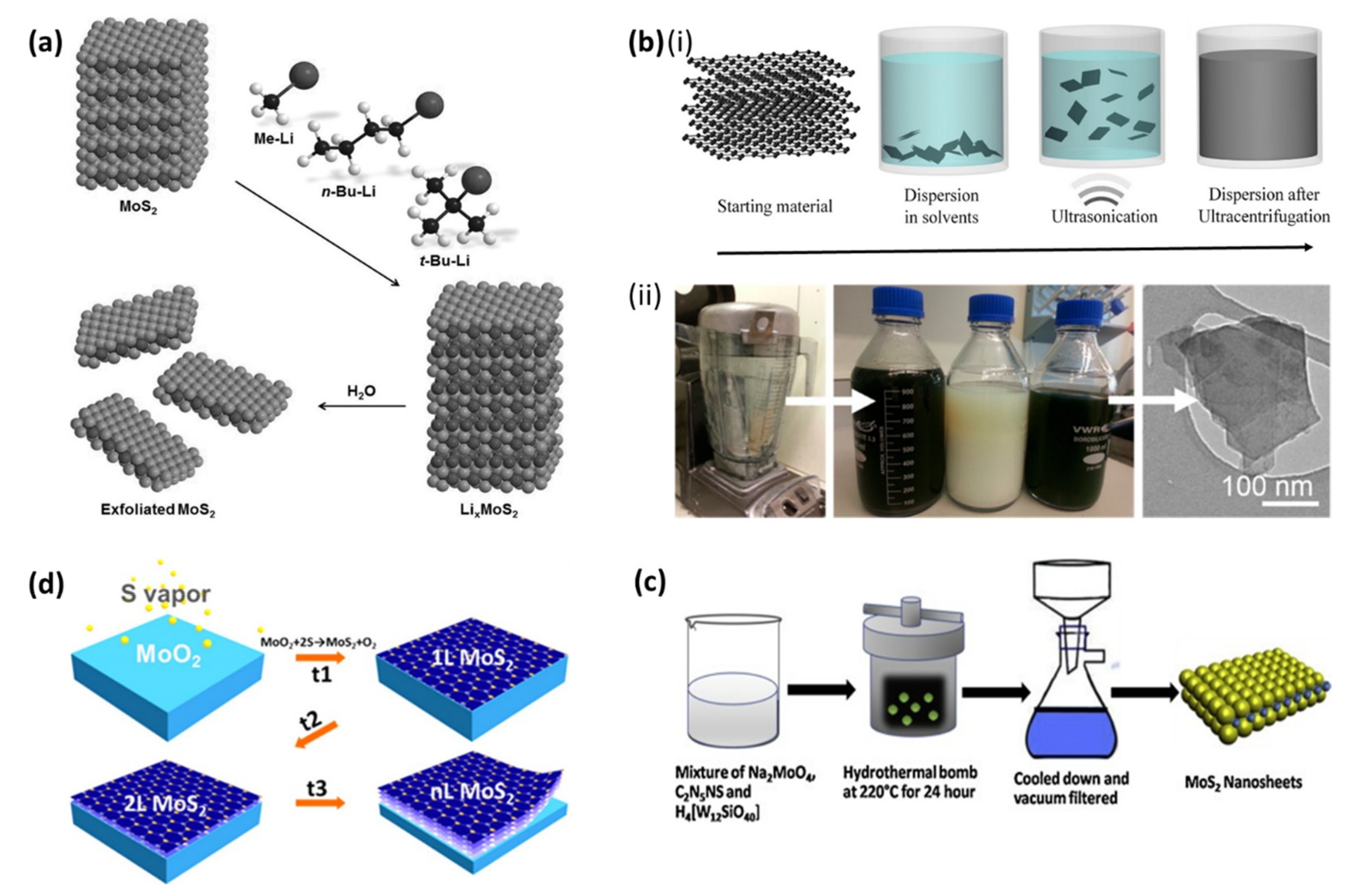
2. Synthesis of MoS2 Nanosheets

Different methods for synthesizing 2D MoS2 nanosheets have been proposed; these methods have also been used for tuning 2D MoS2 electronic band structures. So this creates an opportunity to find new methods that are appropriate for sensing applications. Lately, MoS2 nanosheets have been produced by either mechanical or chemical methods. In a standard mechanical exfoliation procedure, sufficient thin MoS2 crystals are first peeled off from their bulk crystals, layer-by-layer, using adhesive Scotch tape and exerting normal force. By repeating this process multiple times, the bulk MoS2 becomes thinner until it is reduced to a single sheet of MoS2. The cleaved thin crystals are detached with devices, such as plastic tweezers, and are adsorbed onto the target substrate [42]. While this method can yield pristine and high-quality 2D MoS2 nanosheets, poor scalability limits its practical application in general.
Chemical methods include:
(i)
lithium (Li) intercalation exfoliation, which involves an initial 48 h intercalation of Li ions between bulk MoS2 in an inert gas atmosphere followed by a spontaneous ultrasonic-assisted exfoliation of the Li-intercalated MoS2, which occurs through water reaction, as shown in Figure 1a [43,44]. During the process, bulk MoS2 is treated with an n-butyllithium solution to produce the intercalation product LixMoS2. The reaction process is caused by the electron transfer from n-butyllithium to MoS2 layers, which absorbs Li+ between the layers to balance the charge. When the intercalate, LixMoS2, comes into contact with water, it reacts with the intercalated lithium, creating LiOH and H2 gas. As a result, negatively-charged nanosheets repel each other, increasing interlayer distances and weakening van der Waals forces, resulting in a colloidal dispersion of (nearly) entire single layers of MoS2 [45]. The lithium intercalation reaction converts MoS2 from the semiconductive 2H phase hexagonal structure to the metallic trigonal 1T phase [46], although the 1T phase MoS2 is not suitable for optoelectronic devices, it is quite desirable for electrochemical catalysis.
(ii)
Liquid-phase exfoliation (Figure 1b) involves exfoliation by sonication [47,48] or exposure of bulk MoS2 to high shear rates using either a rotor–stator high shear mixer or a basic kitchen blender [49,50]. The bulk MoS2 is exfoliated in the presence of stabilizing liquids, such as suitable solvents [47], surfactant solutions [50], or polymers [51]. Sonication-assisted exfoliation is triggered by hydrodynamic shear forces associated with cavitation, which is the formation, growth, and collapse of voids or bubbles in liquids due to pressure changes [48]. Following exfoliation, the inter-sheet attractive forces and interfacial tension between the sheets and the surrounding liquid are reduced, resulting in the dispersion of a single layer [48]. When using a high shear mixer or blender, exfoliation occurs as a result of revolving rotor–stator blades producing extremely high shear rates [49,50]. The shear rate generates full turbulence, resulting in viscous shear forces. The presence of dominant viscous shear forces increases collision and cavitation between bulk materials, leading to exfoliation [49,50]. During this process, the sheets are coated with an appropriate surfactant/solvent and stabilized by repulsive inter-sheet interactions [50]. This approach results in defect-free single or multilayered nanosheets that are stabilized against aggregation by liquid interaction. The liquid-phase exfoliation method, due to its simplicity and scalability potential, has an advantage over the lithium exfoliation method; it is also not an air-sensitive process and it does not require chemical reactions; thus, it provides high crystallinity for synthesized MoS2 nanosheets [52].
(iii)
Hydrothermal/solvothermal synthesis (Figure 1c) is essentially where the chemical reaction takes place in a closed system (autoclave) in which the solvent temperature is raised to its critical point ( > 200 °C) by heating concurrently with autogenous pressure [53]. This approach involves direct crystallization from solutions, which often include crystal nucleation and subsequent growth [53]. The sample is rapidly precipitated from the reaction solution during the synthesis process, allowing for controlled homogeneity, as well as control over aging, particle size, and morphology [54]. The solvothermal synthesis is similar to the hydrothermal synthesis, except that in the synthetic method organic solvents are used instead of water [55]. MoS2 nanosheets with good crystalline structure and morphology are produced by optimization of hydrothermal temperature and reaction time [54].
(iv)
Chemical vapor deposition (CVD) (Figure 1d) has been used to synthesize high-quality graphene, and it was recently adopted for the synthesis of MoS2 nanosheets. In a standard CVD procedure, molybdenum trioxide (MoO3) and sulfur powders are common precursors used for the deposition of MoS2 films on a silicon/silicon dioxide (Si/SiO2) substrate; upon heating, MoO3 reacts with sulfur vapor in the gas phase at a high temperature ( > 650 °C) to give MoS2 layers in a reducing atmosphere under ambient pressure [56]. The CVD process is capable of producing nanosheets of good quality with scalable size, controllable thickness, and excellent electronic properties. However, it is more difficult to obtain crystalline 2D MoS2 nanosheets with a controlled number of layers by CVD as compared to graphene, because the structure, thickness, and crystallinity of graphene could be well controlled by an effective catalyst design but there is no catalyst involved in the growth of 2D MoS2 nanosheets [56,57].
The important thing to realize is that due to the nature of the exfoliation method, many imperfections, such as surface defects, may occur. The usual defect positions that occur are sulfur vacancies on the surface or edges [58,59]; due to these defects, 2D MoS2 nanosheets have low charge carrier mobility and density [59]. These defects were recognized as possible synthetic targets for the functionalization and modification of MoS2 surfaces for various additional applications [58]. The functionalization of MoS2 is important to adjust or add the required properties to the material, which can be utilized in the fabrication of sensors and catalysts. This is an advantage given that 2D MoS2 offers abundant exposed edges that are known as the root of the catalytic activity [60,61].

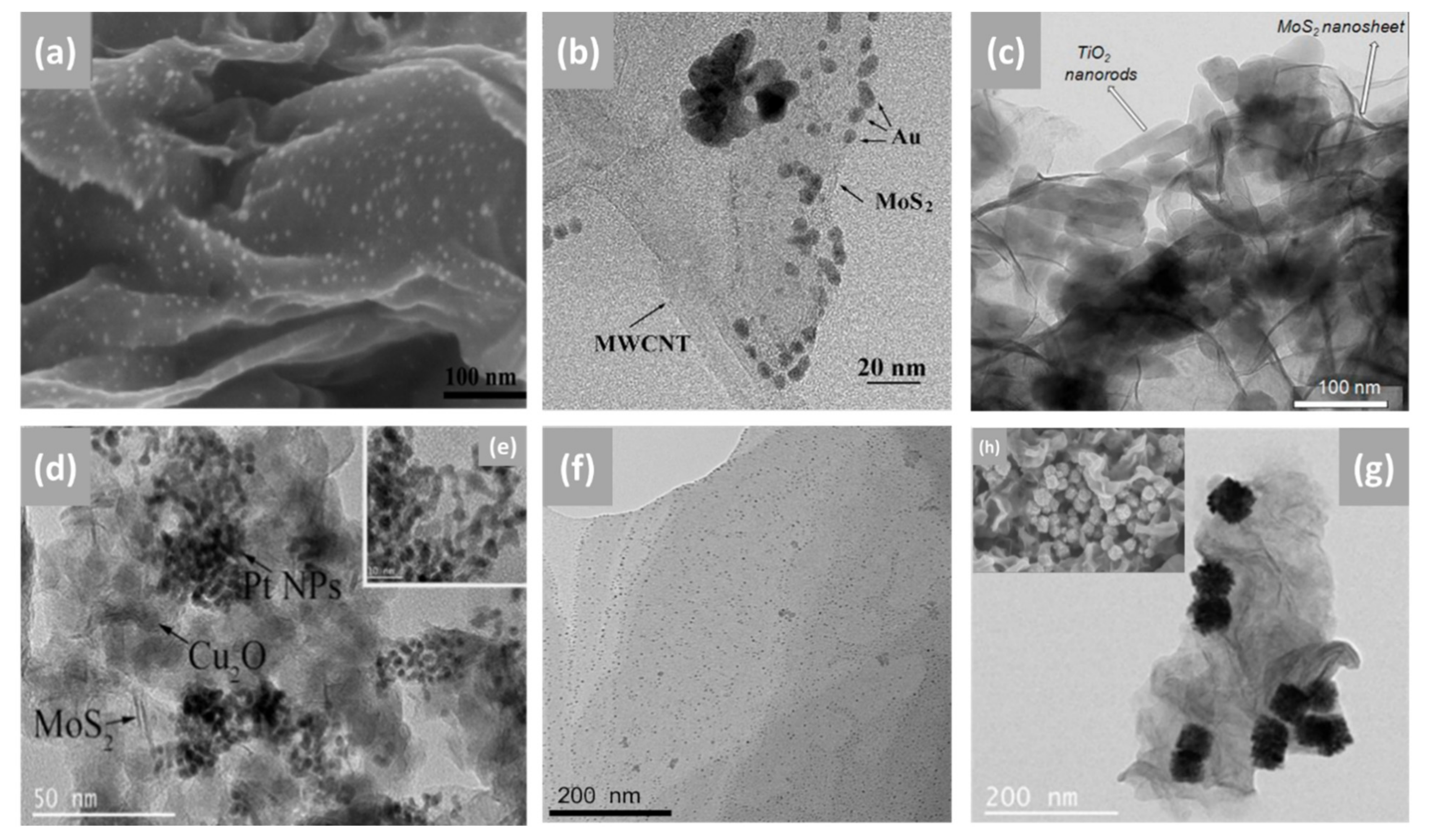
3. Functionalization of MoS2 Nanosheets with Metal and Metal Oxide Nanostructures

Metal and metal oxide NSs are known for their exceptional electrical and catalytic properties; hence, they are the most widely used nanomaterials. The application of these nanomaterials to medicine [62], energy storage, catalysts, sensors [63,64,65], and electronics [66] has led research into the development of synthetic pathways toward the formation of nanocomposites. The integration of these NSs on MoS2 can effectively exploit the distinct qualities of both materials, which have already attracted considerable attention in the sensing field. The metal-based NSs can be distributed and significantly improved by the effective support matrix of MoS2 nanosheets, where the synergistic effects of metal-based NSs and MoS2 nanosheets can lead to greater catalytic efficiency and conductivity than plain MoS2. Several factors play significant roles in the properties of metal and metal oxide NSs, such as crystal structure, size, shape, morphology, and surface chemistry [67]. Thus, structuring methods have been applied to obtain different sizes and shapes of NSs with promising properties, such as high sensitivity, faster electron transfer kinetics, low background currents, high surface areas, and high current densities [68]. Metal and metal oxide NSs have been used to modify electrodes for use as electrocatalysts in sensors; hence, they play significant roles in diagnostic devices. The 2D-MoS2/metal-NS composites utilize the optimum availability of the nanoscale surface area for electron transfer, and also enable mass transport of the reactants to the electroactive focal point on the electrode surface, resulting in a significantly improved electrochemical response [69,70].
The decoration of MoS2 nanosheets with metal-based NSs is commonly carried out in two different ways: in situ or ex situ functionalization. These functionalization methods can be achieved by post immobilization of NSs on MoS2 [69], hydro/solvothermal reaction [70], electrodeposition [13], or the chemical reduction method [35]. In these functionalization methods, the growth control of NSs on MoS2 nanosheets is a prerequisite for tuning the shape, size, and morphology. This growth control however involves precise process monitoring of the experimental parameters, such as the concentration of the reactant, time and temperature of the reaction, pH solution, the surfactant used, and the type of metal salts [71,72]. For instance, in a chemical synthesis process, the size and shape of the NPs can be effectively controlled by the concentration of metal salts, reaction conditions, or the use of different surfactants. Moreover, through an electrochemical synthesis, the concentration of surfactants, growth temperature, and current density can be optimized to control the size and shape of the NPs [72]. Concerning the subject, a study was conducted where thionine (C12H10N3S+)-MoS2 was functionalized with AuNPs by a hydrothermal reaction for electrochemical immunosensing [73]. C12H10N3S+ was used as a reducing agent and a surfactant to tune the resulting AuNPs structures on the surface of the MoS2 nanosheets. The study demonstrated that various well-defined shapes of AuNPs were produced by adjusting the concentration of C12H10N3S+ while the concentration of metal salt (HAuCl4) remained constant. It was discovered that with an increasing concentration of C12H10N3S+, the size of the NPs increased and the shape changed from spherical, triangle, and clover-like to flower-like shape. A significant finding was that C12H10N3S+ could not facilitate the growth of AuNPs in the absence of MoS2 nanosheets. This indicated that C12H10N3S+ and MoS2 had a synergistic effect on the formation of AuNPs and the growth of AuNPs was also promoted by the effective support matrix of MoS2 nanosheets. The proposed mechanism was because C12H10N3S+ is an electrochemical indicator, the growth of AuNPs on the surface of MoS2 nanosheets could be due to the redox reaction among MoS2, C12H10N3S+, and AuCl4. C12H10N3S+ was absorbed on the surface of MoS2 nanosheets through a π π   interaction and an electrostatic interaction due to its planar aromatics structure. Therefore, MoS2/AuCl4 and C12H10N3S+/AuCl4 formed two redox pairs, enabling the spontaneous transfer of electrons from MoS2 and C12H10N3S+ to Au ions, allowing the reduction of Au ions to AuNPs on the MoS2 nanosheets [73,74,75].
Recently published reviews have reported on the synthesis and application of metal and metal oxide NSs [72,76]. The reviews included extensive information on the effects of structural morphology, size, and shape on the properties of NSs and their application in the field of electrochemical sensors. Interestingly, all studies clearly indicate that the shape and structural morphologies of NSs serve important roles in determining their resulting electrocatalytic properties, as the number of exposed catalytic active sites is specifically dependent on the shape of the NPs. That being said, it was also reported that a perfect shape–surface structure interaction is unrealistic and, even with a well-defined size and shape, its surface will be extremely complex. It consists of not only some ordered surface domains of different dimensions but also a defined number of defects, corners, edges, steps, and kink sites, all of which contribute to the resulting electrocatalytic activity [77].
Many methods for the preparation of size and shape-controlled metal-based NSs are now available in the literature. Various sizes, shapes, and structures can be synthesized, such as 0D NSs, which include structures, such as NPs, quantum dots, and nanospheres, as well as 1D NSs with high aspect ratios, such as nanorods, nanocombs, nanofibers, nanotubes, nanoneedles, nanoribbons, and nanowires. The 2D NSs are known as nanoplates, nanosheets, and nanopellets, while nanocrystals, multi-nanolayers, nanoflowers, and snowflakes are characterized as 3D NSs [76,78]. A comprehensive effort has been made to control the shapes and sizes of metal-based NSs in order to guarantee their efficient performances in electrochemical sensors. The synthesis of various forms of NSs not only enhances physical and chemical properties but also improves the biocompatibility and bioefficacy for the immobilization of biomolecules [72,76,79]. Moreover, due to the many active sites provided by particular NSs, a wide linear range and low detection limits have been achieved, resulting in NSs being ideal materials for the fabrication of biosensor devices. Table 1 summarizes the various functionalization methods of MoS2 nanosheets with different metal and metal oxide NSs, their resulting structural morphologies (size and shape), and their application in electrochemical sensors. The commonly used technique for making 2D-MoS2/metal-NSs composites is in situ chemical growth.

3.1. Ex situ Functionalization

Ex situ functionalization (post immobilization) requires the mixing of a MoS2 nanosheet solution with pre-synthesized NPs to form a composite. Even though the NPs and 2D material suspensions are independently pre-synthesized, the ratio of the two materials can be controlled with precision [110]. In this method, NPs are synthesized in advance and then attached to the MoS2 surface through covalent [80] or noncovalent interactions, such as van der Waals or electrostatic interactions, and hydrogen bonding [111]. The ex situ functionalization by absorption is much easier, more flexible, and ideal for commercial applications on a large scale than the in situ functionalization procedure. The deposition of metal NSs on the surface of MoS2 is determined by the type of bonding and, thus, the strength of interaction. In covalent functionalization, the metal-based NSs are attached to the edge and surface of MoS2 through covalent bonding between metal atoms of NSs and sulfur atoms of MoS2 [15,80]. The sulfur vacancies on MoS2 are created by severe defects and edges caused by the loss of atoms during the intense chemical exfoliation [112]. The vacant sulfur atoms that bind to metal atoms serve as sites for metal nuclei seeding and subsequent growth into larger NSs [15,111]. The covalent bonding of NSs usually results in a strong and stable attachment that prevents the leaching of particles. The main advantage of covalent bonding is that it uses efficient and controlled chemical interactions to avoid side reactions and prohibits undesirable formations [113]. Alternatively, metal NSs can be attached to MoS2 via noncovalent interactions. Electrostatic interactions are the commonly utilized noncovalent approaches in the syntheses of MoS2-based nanocomposites [69,81,82]. Absorption of MoS2 is often achieved via surfactant functional groups attached to the surface of metal and metal oxide NSs. The negatively charged MoS2 nanosheets are then leveraged to electrostatically interact with positively charged metal-based NSs, resulting in strong interactions and high particle loading [69,114]. Non-covalent functionalization provides the advantage of allowing metal NSs to be introduced into MoS2 without changing its structure, preserving the unique features of 2D MoS2 [110,111]. Based on the above-mentioned interactions and the nature of the attached NSs, the optical, catalytic, and electrical properties of MoS2 could be improved. For instance, electrostatic interactions offer more conductive interlayers for electron transfers between MoS2 nanosheets and absorbed metal NSs, resulting in better electronic characteristics of MoS2 [69]. Covalent bonding, on the other hand, offers a high density of active sites and a large surface area by the strong and stable attachment of metal NSs and induced surface defects, thereby enhancing the catalytic activity of the MoS2 nanosheets [115,116].
The main challenge aimed at ex situ functionalization is the ability to synthesize NPs that have high dispersibility and long-term aggregation stability. The uniform distribution of NPs is mostly hindered by phase separation, segregation, and agglomeration, which deteriorate the properties of the material. The use of capping agents and surfactants helps prevent particle agglomeration and reduces any phase separation due to the material’s incompatibility. Owing to electrostatic interactions, the polar groups of surfactants can be adsorbed on the surface of NPs [117]. Surfactants can reduce particle–particle interactions and, thus, decrease the formation of agglomerates as physical attraction forces decrease [118]. However, a downside of using surfactants is that they are thermally and solvolytically unstable because of the relatively weak van der Waals forces or the hydrogen bond that binds them to the surface of NPs [117]. It remains a challenge to achieve a homogeneous dispersion of non-agglomerated NPs in the nanocomposite matrix by the typical ex situ functionalization method; hence, researchers tend to also use ultrasonication techniques to disperse NPs on 2D materials. For example, Au nanoparticles were immobilized on the MoS2 surface by ultrasonication for the fabrication of electrochemical biosensors [69,80]. The transmission electron microscope (TEM) image verified the immobilization of Au nanoparticles in close proximity to each other on MoS2 nanosheet surfaces via covalent bonding between Au atoms and sulfur atoms (Figure 2b) [80]. This was due to the direct surface affinity between the integrated structures of MoS2 and the Au nanocrystals. In yet another instance, an electrochemiluminescence immunosensor was fabricated based on MoS2-PEI-Au nanocomposites formed through the dispersion of MoS2-PEI into Au NPs by stirring the solution overnight (Figure 2c) [81]. Au NPs were distributed randomly on the layered surface structures of MoS2 nanosheets. On the other hand, the MoS2-CuO nanocomposite (Figure 2d) obtained by stirring the two nanomaterials for hours showed the reduced CuO nanotube aggregation [82]. The agglomeration of the NPs may appear to have had negative impacts on the properties of the nanocomposite. However, in a rare instance, agglomeration of Au NPs on the surface of MoS2 was discovered to be particularly favorable for enhancing the photocurrent response of MoS2 based on the effects of surface plasmon resonance [80]. Combined with thin layers of 2D MoS2, they efficiently transformed the local plasmonic enhancing effect into an electrical signal, thus improving the photoelectrochemical response of MoS2 [80]. Figure 2 shows the TEM images of 2D-MoS2/metal-NSs composites produced by the ex situ functionalization method; the NPs exhibited some agglomeration and displayed a non-uniform coverage. It should be noted that the arrangements of the NSs on the surface and within the MoS2 nanosheet matrix depend greatly on the functionalization process.

3.2. In Situ Functionalization

The in situ functionalization is the most commonly used approach and an effective way of preparing nanocomposites based on 2D MoS2 decorated with metal-based NSs. In this technique, the NPs are synthesized within the matrix or the surface of MoS2 nanosheets from metal salts that are converted into required NPs by order of reduction reactions.
This approach has the advantage of preventing particle agglomeration while improving the overall spatial distribution of NPs. The in situ functionalization has gained attraction over ex situ functionalization because it provides greater control over the material’s structure and properties, and particle size can be regulated with minimal effort. The in situ approach is more cost-effective and has an inherent benefit that the interfaces of the nanocomposite matrix are clean, resulting in good interfacial bonding. NPs are frequently produced at the active sites or the edges of MoS2 during the reaction in situ functionalization, resulting in increased catalytic and electronic properties [119]. In situ synthesized NPs are smaller in size and are more uniformly dispersed in the matrix, resulting in better mechanical properties [120,121]. Improved spatial distributions of NPs on the surface of the MoS2 nanosheet not only increase the synergistic effect and active surface area but also have the potential to control the charge carrier density [88,122]. As a result of enhanced electrical conductivity and electron mobility, as well as a large active surface area, biological molecules can be effectively immobilized on MoS2 for the detection of target analytes [123].
The benefit of the in situ approach is the prospect of using a range of chemical synthesis approaches, including deposition methods, hydrothermal/solvothermal techniques, sol–gel synthesis, etc. [111]. Unlike ex situ functionalization, it is possible to avoid the use of surfactants and capping agents during the in situ synthesis of NPs. The drawback of this method is that the unreacted precursors or by-products of the in situ reactions might influence the properties of the final material [124,125].
Among various articles published on the in situ preparation of numerous different nanocomposites in the application of electrochemical sensors, electrodeposition is among the most commonly used method for surface modification. Electrodeposition uses electrical currents to reduce metallic ions from the electrolyte solution of a specific material and coat the material as a thin film onto a conductive substrate surface (electrode) [126,127,128]. Overall, the electrodepositing process may either be: (i) an anodic process in which a metal anode in the solution is electrochemically oxidized, reacts together, and then deposits on the anode; or (ii) a cathodic process in which components (ions, clusters or NPs) are deposited from solution precursors onto the cathode [128]. This method has already been used for the deposition of the NPs on the 2D MoS2 surface [83,84,85,86]. The most significant feature of the process is that the morphology and film thickness of NPs can be conveniently tuned by adjusting the experimental parameters, for instance, the film thickness of NPs can be regulated by the electrodeposition time, and the rate of deposition can be influenced by the current changing over time [128]. Moreover, Bera et al. [129] mentioned that the ultimate size distribution of the electrodeposits is strongly dependent on the kinetics of the nucleation and growth. Furthermore, during the process of electrodeposition, the nucleation of NPs on the electrode substrate is determined by the structure of the substrate, specific free surface energy, adhesion energy, and lattice orientation of the electrode surface [129]. Additionally, this single-step method has some benefits, such as low-cost equipment, a relatively low processing temperature, short deposition time, and reduced material waste [130,131]. It has been reported that electrodeposition is a better method compared to drop casting when it comes to electrode modification. The biosensor prepared by the electrodeposition method has a fast response time, and a 50-fold lower detection limit compared to the biosensor prepared by the drop casting method. Other attributes include high reproducibility, long-time storage stability, and adequate selectivity, suggesting that the electrodeposition of the nanocomposite provides a promising route to novel types of highly sensitive and stable electrochemical biosensors [132]. Su et al. [13], fabricated an electrochemical aptasensor based on Au NPs decorated on MoS2 nanosheets. The Au-MoS2 nanocomposite was formed by the electrodeposition of Au NPs on MoS2 nanosheets. After an electrodeposition cycle, the scanning electron microscope (SEM) image (Figure 3a) showed that Au NPs with an average diameter of 10 nm were distributed homogeneously over the surface of MoS2 nanosheets, indicating that the MoS2 was successfully functionalized. Zhang et al. [83] developed an electrochemical sensor for the detection of nitrite by electrochemical deposition of Au NPs onto the surface of MoS2-MWCNT nanocomposite. As shown by the TEM image in Figure 3b, Au NPs with sizes ranging from 3 to 5 nm were successfully grown on the MoS2-MWCNT nanocomposite. However, the Au NPs were not evenly distributed and showed some agglomeration.
Other popular methods for the functionalization of 2D MoS2 nanosheets with NSs include hydrothermal/solvothermal and chemical reduction. Hydrothermal/solvothermal syntheses are described as conducting chemical reactions in solvents placed in sealed vessels in which solvent temperatures can be brought up to their critical points by heating concurrently with autogenous pressures; the method is known as hydrothermal when water is used as a solvent [133,134]. Syntheses of materials by hydrothermal/solvothermal methods involve crystallization directly from solutions that typically require two steps: crystal nucleation and subsequent growth. The resulting nanomaterials may be produced with required particle sizes and morphologies by regulating processing variables, such as temperature, pH, reactant concentrations, and additives [53]. Figure 3c exhibits reported TEM results of MoS2 nanosheets decorated with titanium dioxide (TiO2) nanorods by the hydrothermal process. The MoS2-TiO2 nanocomposite image showed that the uniform cylindrical TiO2 nanorods with an average diameter of ~20 nm and length of ~180 nm were incorporated and partially dispersed into the MoS2 nanosheets [106]. In another study, MoS2 nanosheets were functionalized by the solvothermal reaction and post-immobilization process. Firstly, MoS2 nanosheets were coated with 15 nm Copper(I) oxide (Cu2O) NPs via solvothermal synthesis, the synergistic interaction between MoS2 and Cu2O facilitated the formation of a homogeneous structure of a small particle size, as shown in Figure 3d. Formation of MoS2-Cu2O/Pt nanocomposite was by post immobilization of a platinum (Pt) NP solution under ultrasonic conditions. From the reported TEM results (Figure 3d,e), Pt NPs with an average diameter of 3 nm were partially dispersed on MoS2-Cu2O nanocomposite [70].
Some researchers opt for chemical reduction syntheses for the functionalization of MoS2 nanosheets. For instance, Figure 3f,g exhibit the reported TEM results of a 2D MoS2 nanosheet decorated with silver (Ag) NPs and PtPd bimetallic nanocubes (PtPd NCs), respectively. The insert image (Figure 3h) is the SEM image of MoS2-PtPd. Ag NPs (diameter 3 nm) were homogeneously dispersed on the surface of the MoS2 nanosheet and there were none of the Ag NPs outside the nanosheet, which could be due to enhanced MoS2 surface activity resulting from binary co-doping of nitrogen fluorine elements [64]. On the other hand, PtPd NCs with an average side length of about 50 nm were partially distributed on MoS2 nanosheets, and the surface of PtPd NCs was not smooth, as it consisted of smaller NCs instead of cubic nanosheets [96]. The chemical reduction method is highly favored because it is simple, cost-effective, and has the advantage of producing NPs without aggregation. Moreover, it can achieve better particle size and distribution control by simply optimizing the experimental parameters, such as the molar ratio of the capping agent with the precursor salt and the ratio of the reducing agent with the precursor salt [135]. This method includes the reduction of metal salt in a suitable medium in the presence of a surfactant/stabilizer and a reducing agent [136,137].
While researchers aim for the functionalization of 2D MoS2 nanosheets to broaden their prospective applications, it is important to note that control of catalytic, electronic, and optical properties of these nanomaterials during production is crucial for device applications, irrespective of the method of synthesis and functionalization.

4. Properties

The 2D nanomaterials are known to have special properties, which are distinct from their 3D bulk counterparts. The 2D MoS2 nanosheets with completely tunable properties can be synthesized successfully with various types of methods as discussed above. Due to changes in properties with a decrease in the number of layers, 2D MoS2 nanosheets possesses significantly distinctive electrical, optical, and chemical properties, which are known to play important roles in the fabrication of sensors. The exceptionally large surface areas of 2D MoS2 nanosheets offer robust surface functionalization and provide new possibilities for functional devices based on 2D materials. MoS2 has been reported to simply form nanocomposites with metal and metal oxide NSs [69,82], carbon nanomaterials [137,138], conductive polymers [139,140,141], and other 2D nanomaterials [142,143], which could be used as catalytic materials to significantly increase the electrochemical performance of sensors based on MoS2-nanocomposites. The 2D MoS2/metal-NS composites have the inherent properties of pure metal NSs and MoS2 nanosheets due to their synergistic effects, which makes the 2D MoS2/metal-NS composites exhibit outstanding electrochemical properties and improved sensitivity [13]. Through studying Zhang’s review paper [8], one can find comprehensive insights into MoS2 nanosheets used as building blocks or supports for the preparation of MoS2 nanosheet-based composites with other materials.

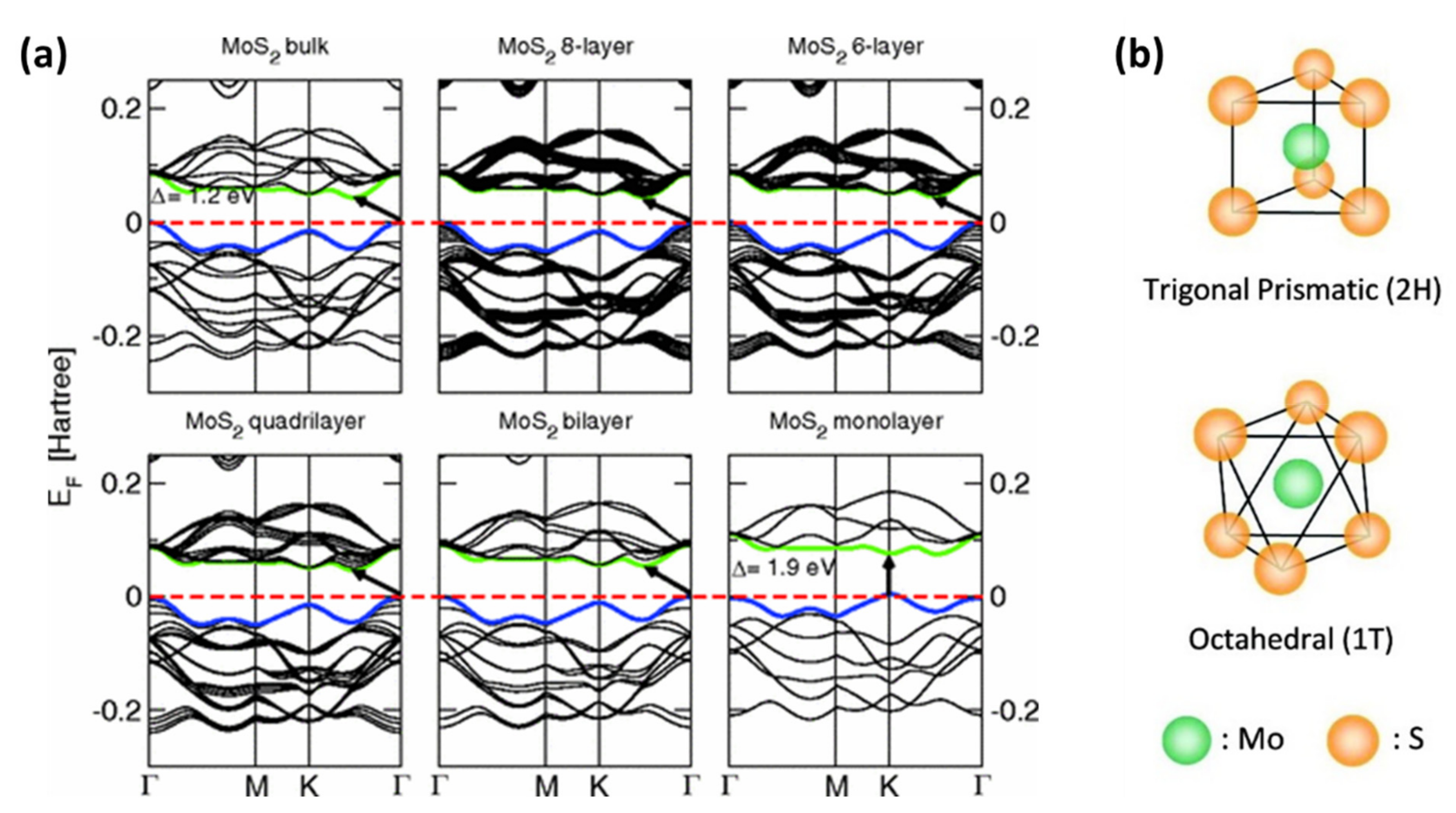
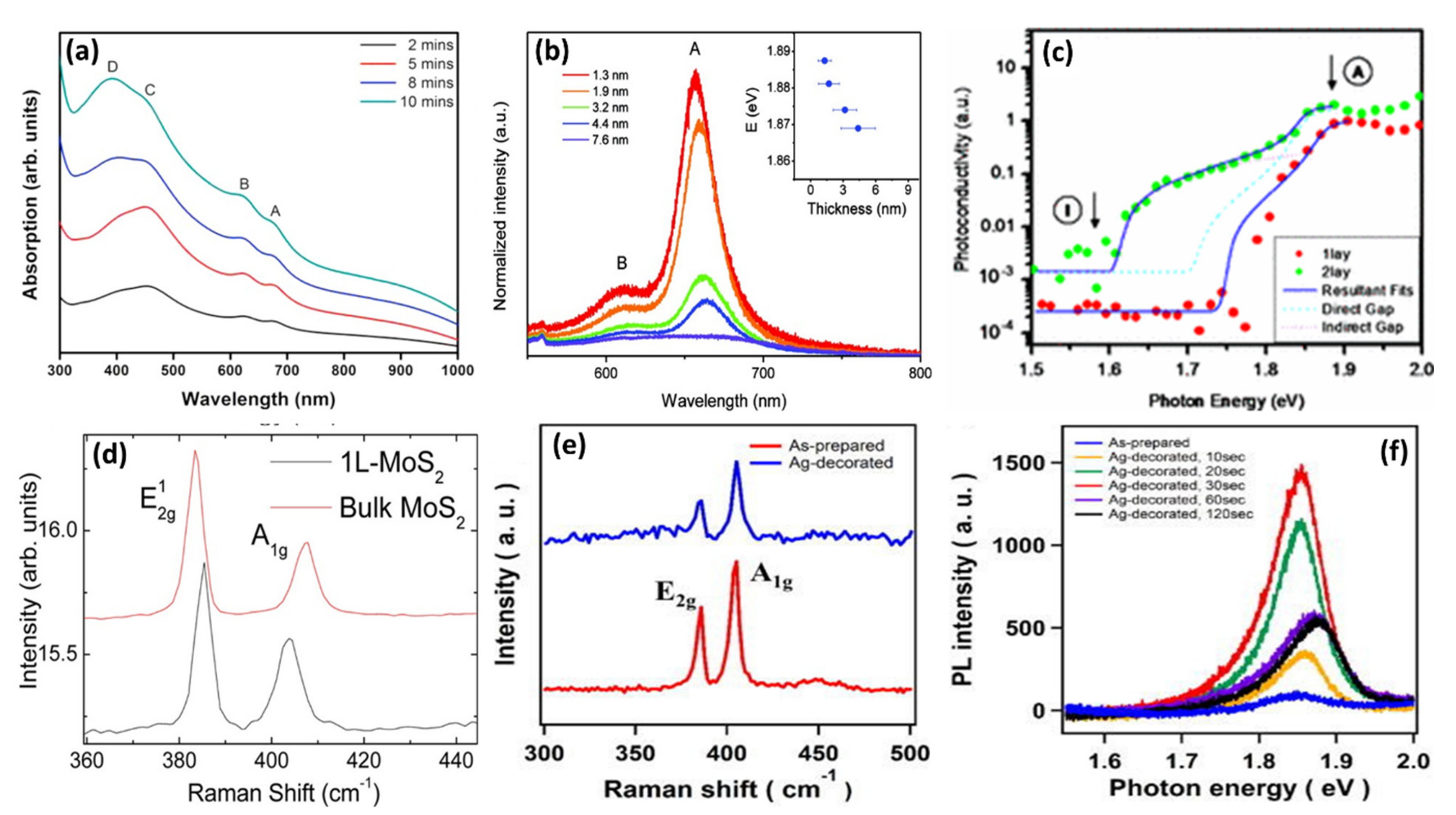
4.1. Electrical Properties

The bulk MoS2 is considered to have low electrical conductivity and high electrical resistivity mainly due to its intrinsic structure, where single sheets of MoS2 are stacked together and bonded by week van der Waals interactions between adjacent single sheets. However, 2D MoS2 has a unique morphology and electrical properties with efficient transmission of electrons on account of the direct energy band structure. Thus, an understanding of the electronic structure of 2D MoS2 layers is of great importance. For instance, changes in the interlayer coupling, degree of quantum confinement, and symmetry elements result in significant differences in 2D MoS2 electronic structure relative to bulk MoS2 [9,144,145,146]. The electronic structure of the single-layer and few-layer MoS2 and the resulting special optical properties arise from the configurations of the d -electron orbitals that comprise the MoS2 conductive and valence bands [147,148]. The outer d-electron interactions give rise to a band gap of ~1 eV between the occupied and unoccupied “d” states of single-layer MoS2, which make them different from other sp -bonded semiconductor nanostructures [9,149]. TMDs have diverse electronic properties that emerge from the gradual filling of non-bonding d bands from group 4 to group 10 transition metals. When the orbitals are partially filled, as in the case of 2H-NbSe2 and 1T-ReS2, TMDs exhibit metallic conductivity. When the orbitals are fully occupied, such as in 1T-HfS2, 2H-MoS2, and 1T-PtS2, the materials are semiconductors [149]. The MoS2 band structures can be calculated from the first principles of the density functional theory (DFT) in order to obtain more information regarding their electronic structure.
Kadantsev et al. [145] investigated the electronic structure of a single-layer MoS2 with all electron first-principle calculations based on DFT and variational treatments of spin-orbital coupling. Another detailed study was conducted on the effect of quantum confinement on the electronic structure of single-layer and few-layer MoS2. The reported results indicated that the band gap of the bulk MoS2 stemmed from the transition from the top of the valence band situated at Γ to the bottom of the conduction band halfway between the Γ and K high symmetry points, and the optical direct band gap of the single-layer MoS2 was situated at K point [146]. The conductive band states at the K point consist mainly of highly localized d orbitals at the Mo atom sites located in the middle of the S-Mo-S unit cell and they have minimal interlayer coupling [148]. However, the states near the Γ point are attributed to a linear combination of d orbitals on Mo atoms and antibonding pz orbitals on S atoms and they have strong interlayer coupling with energies that depend sensitively upon the thickness of the layers [148]. Figure 4a illustrates the band structures obtained for bulk to 2D MoS2. The trend observed is that the direct excitonic transition energy at the Brillouin zone K point hardly changes with the thickness of the layers; however, decreasing the number of layers leads to a gradual shift in the indirect band gap to a high direct band gap in mono-layers that the material turns into a 2D semiconductor [146,148]. This shift from the bulk indirect band gap to a single-layer direct bandgap results from the effects of quantum confinement [144,146].
In addition to studying the electronic structures of the bulk MoS2 and the 2D MoS2, the fundamental experiments and theoretical studies have suggested that other variables may affect the material’s electrical properties, such as preparation methods [44,150,151,152], functionalization or doping [122,153,154,155,156], and environmental conditions [157]. For instance, many CVD-based methods for the synthesis of 2D MoS2 have been developed, and changing experimental conditions, such as varying degrees of MoO3 sulfurization during formation, can affect the material’s optical and electrical properties [150]. As reported, the Li intercalation of MoS2 leads to the structural transformation of MoS2 from the 2H phase to the 1T phase (Figure 4b) triggered by the charge transfer from Li to MoS2 [149], as well as a transition from semiconductor to metallic 2D MoS2 nanosheets [43,44,46]. The intercalation process usually produces negatively charged nanosheets with different properties from their neutral counterparts. The antibonding d-orbitals of the transition metals are filled leading to different electronic properties, such as the change from semiconducting nanosheets to metallic [158]. Ambrosi et al. [44] studied the influence of Li intercalation on the electrochemical properties of exfoliated MoS2 nanosheets. The electrochemical measurements were conducted with a MoS2-modified carbon electrode (vs. Ag/AgCl reference electrode) using the cyclic voltammetry (CV) method over a potential range of −1.6–1.4 V. From the results obtained, n / tert -butyllithium (Bu-Li)-exfoliated MoS2 exhibited a large current density with oxidation and reduction peak intensities almost three times greater than the bulk material. These intrinsic electrochemical properties of exfoliated MoS2 have significant implications as they could create new opportunities in the field of electrochemical sensing and biosensing where the anodic and cathodic signals from MoS2 can be used as identification and quantification tags [44]. The major influence on 2D MoS2’s electrical properties could also be due to considerable environmental effects, and such effects could greatly restrict the exploration of 2D MoS2’s inherent properties. Khan et al. [157] studied the electrical and photoelectrical properties of MoS2-based field effect transistors (FETs) in the dark and in the presence of deep ultraviolet (DUV) light under various environmental conditions (vacuum, N2 gas, air, and O2 gas). The results obtained showed the difference in device performance. In the dark, the environmental gases did not modify the Ion/Ioff of the device; however, the environmental gases changed the characteristics of the device under DUV illumination. Further studies were also carried out to evaluate the influence of temperature and pressure on the electrical conductivity of 2H-MoS2 [159,160].
While many other relevant studies are being conducted on MoS2 electrical properties, there are very few detailed studies focused on the effects of doping or functionalization on optical and electrical properties of bulk and 2D MoS2. Doping or functionalization are considered some of the most common ways to alter the band structures of semiconductor materials [161]. The large surface areas of 2D materials offer effective surface functionalization and create new possibilities for functional devices. In particular, MoS2 functionalized with metal-based NPs was found to have additional benefits in potential applications, such as electrochemical sensors [69,108].
When it comes to electrochemical sensors, researchers typically use electrochemical techniques, such as CV, to study electron transfer kinetics, and electrochemical impedance spectroscopy (EIS) to study the charge transfer resistance (Rct) of the material on the electrode surface in K3[Fe(CN)6]/K4[Fe(CN)6] electrolyte. Song et al. [88] utilized nitrogen fluorine pre-doped 2D MoS2 nanosheets decorated with Ag NPs (Ag NPs-N-F-MoS2). Upon characterization with EIS, he found a decrease in Rct of the AgNPs-MoS2 (40 Ω)-modified glassy carbon electrode (GCE) as compared to the non-functionalized MoS2 (220 Ω) (Figure 5a,b).
These findings indicate that the synergistic effect between MoS2 nanosheets and Ag NPs has induced enhancement of the signal and increased electrical conductivity, suggesting that MoS2 electrical properties can be effectively tuned by incorporating Ag NPs with MoS2 [88]. Similar results were observed with CV characterization (Figure 5c). The CV responses of modified electrodes showed typical K3[Fe(CN)6]/K4[Fe(CN)6] redox peaks with narrow peak-to-peak potential separations. The fast electron transfer rate was obtained at the AgNPs-MoS2-modified electrode, indicating a good electrical conductivity of the AgNPs-MoS2 nanocomposite. The most intriguing finding was an increased electron transfer rate and a low Rct (15 Ω) response in Ag NPs-N-F-MoS2. This suggests that non-metal dopants affect the electrical characteristics of MoS2. Theoretical calculations in the study revealed that nitrogen fluorine pre-doped 2D MoS2 nanosheets had smaller bang gaps (0.8 eV) than pristine MoS2 nanosheets (1 eV). This proved that by doping MoS2 nanosheets with non-metal dopants, excellent intrinsic conductivity could be achieved. Furthermore, doping allowed for good interfacial bonding and monodispersity of Ag NPs on N-F-MoS2, increasing the surface area and preventing side reactions. As a result, excellent conductivity, exceptional electron mobility, and fast mass transport were achieved.
In another study, MoS2 nanosheets functionalized with Au-Pd bimetallic NPs were applied and tested for the interface properties of modified electrodes using EIS (Figure 5d). The reported results showed that electrodes modified with MoS2 had a high Rct of 1373 Ω due to poor conductivity and negative MoS2 nanosheets charges. After post-electrode modification with Au-Pd/MoS2 nanocomposites, Rct was significantly reduced due to the excellent conductivity of bimetallic Au-Pd NPs. The CV (Figure 5e) results matched those of the EIS. MoS2 nanosheets exhibited low current responses compared to Au-Pd/MoS2 nanocomposites with significantly higher current responses [89]. It was reported that the NP coverage on the MoS2 nanosheet surface has the ability to control the charge carrier density, which could have a major effect on MoS2-based sensor fabrication and device optimization [153]. Chamlagain et al. [153] studied the control of interfacial charge transfer and tailoring of the electronic charge transport properties of the MoS2 FET based on the functionalization of MoS2 by varying the coverage of Au NPs on the MoS2 surface. The results showed increasing Au NPs coverage; the threshold voltage of the MoS2 FET showed a continuous positive change from 4 to 41 V, resulting in a tunable charge transfer of 3.5 × 10¹¹/cm2 to 4 × 10¹²/cm2. The carrier mobility also varied from 52.5 to 2.8 cm2/VS with Au NP coverage. Another study indicated that doping induces large variations in the electrical properties of 2D TMDs [122]. The electrical properties (e.g., resistivity) would largely depend on the numbers and positions of the dopant atoms in 2D TMDs, which is very challenging due to the diffusion laws and the statistical complexity of dopant distribution [122]. However, there is still a lack of intensive research on the effect of NP coverage on the MoS2 surface and the role of dopant atoms on electrical properties in 2D TMDs.

4.2. Optical Properties

MoS2 nanomaterials have since surfaced as potential materials for several applications in optical devices due to their impressive optical properties. The direct 1.9 eV optical gap in 2D MoS2 results in an electron–hole pair excitation that could be used in LEDs, photodetectors, and other photonic devices [147,162]. The stability of MoS2 towards photocorrosion is beneficial in photochemical reactions and the tunable band gap indicates that the material can harvest light over a wide range, from ultraviolet to infrared wavelengths [149]. The stability of MoS2 towards photocorrosion is considered to be due to its antibonding characteristics. According to the extensive dichalcogenide band structure calculations, the relevant Γ4 state at the top of the valence band is not a non-bonding metal d state but rather an antibonding state between metal d z 2 and non-metal p z   orbitals [162]. There are several factors that can directly influence MoS2’s optical properties, such as the electronic band structures, as described previously, quantum confinement effects, and functionalization or doping [6,149,155,162]. The quantum confinement triggers a distinct change in electronic or optical properties in nanomaterials [163]. The quantum confinement effect has been reported to induce a strong blue shift as large as 4 eV in MoS2 optical absorption features when the lateral dimensions of the MoS2 nanostructures are reduced to nanometers [147,162,164]. These unique optical properties come from the d -electron orbitals that dominate the valence and conduction bands [146]. Extensive experimental studies have been carried out using spectroscopic techniques, such as optical absorption, photoluminescence (PL), photoconductivity, spectroscopic ellipsometry (SE), and electroluminescence to better understand the optical properties of bulk and single-layer MoS2 [46,144,165,166,167]. The Raman signal is also used to confirm the atomic structural arrangement of MoS2 and to provide potential explanations of layer-dependent optical properties [15,54,148,152]. The increase in bandgap energy due to the change in indirect to direct bandgap induces changes in absorption spectra. Figure 6a shows the optical absorption spectra of MoS2 deposited on a SiO2/Si substrate with varying atomic layer thicknesses using a chemical bath deposition (CBD) technique. The thicknesses of the atomic layers increased as the deposition time increased from 2 to 10 min. The number of layers ranged from 2, 3, 4, to a few layers, with time varying between 2, 5, 8, and 10 min, respectively. The optical absorption spectra exhibited two distinctive absorbance peaks assigned to exciton bands A and B between 600 and 700 nm [46,167,168]. These excitonic peaks were considered to result from direct gap transitions between the maxima of split valence bands and the minimum of the conductions all positioned at the K point of the Brillouin zone [144,148]. However, only a slight change in absorption peaks from the direct excitonic states was observed with change in the number of MoS2 layers [144,148]. The A and B exciton peaks in the single-layer MoS2 were found to shift upwards in energy relative to those of the bulk counterpart and had smaller separation due to reduced interactions between the layers [169]. The C and D absorption peaks may be attributed to the direct transition from the deep valence band to the conduction band [168]. In PL studies, it was discovered that the photoluminescence of MoS2 increased with a decreasing number of layers/layer thickness, and that the luminescence from a single-layer MoS2 is more enhanced, whereas in bulk material it is absent [6,144,148]. Figure 6b shows the PL spectra of MoS2 thin layers with thicknesses ranging from 1.3 to 7.6 nm (single layer ~ 0.65 nm thickness, (6.5 Å)). The energy of the A exciton peak as a function of average layer thickness is shown in the inset. The PL spectrum of MoS2 exhibits one enhanced peak and one small peak at around (A) 660 nm (1.9 eV) and (B) 610 nm (1.77 eV), respectively. These emission peaks are in perfect alignment with the energy of the excitons A and B [46]. The enhanced peak relates to the band gap of the materials, and the small peak may be due to the valence band splitting triggered by strong spin–orbit coupling, which corresponds to the direct excitonic transition at the K point of the Brillouin zone of MoS2 [168]. The photoluminescence behavior of this material suggests that the luminescence quantum efficiency is much higher in single-layer/few-layer MoS2 than in multilayer MoS2 [148].
The photoconductivity of these materials also show characteristics related to the band structure. According to the photoconductivity results (Figure 6c) by Mak et al. [144], the conductivity of MoS2 increases steadily with respect to photon energy towards the direct band gap, as anticipated for an indirect band gap material. These characteristics indicate that bilayer MoS2 is an indirect band gap semiconductor, whereas single-layer MoS2 is a direct band gap material [151]. Splendiani et al. [148] observed PL and Raman signal dependence on MoS2‘s number of layers. The Raman features, i.e., the frequency, intensity, and width of the peaks, are highly influenced by the number of layers. Raman spectrum in Figure 6d exhibits two main peaks at 385 cm−1 and 404 cm−1 corresponding to the in-plane ( E 2 g 1 ) vibrational mode of S atoms and out-of-plane ( A 1 g ) vibrational mode of Mo and S atoms, respectively [167,168]. The frequency of the A 1 g vibrational mode increases as the number of layers of MoS2 increases to bulk, while the frequency of the E 2 g 1 vibrational mode decreases [165,169]. Moreover, a blue shift is observed with the A 1 g vibrational mode, while the E 2 g 1 vibrational mode displays a red shift. The shift in frequencies was attributed to long-range Coulombic interlayer interactions and the influence of stacking-induced structural changes [170]. A review by Ye et al. can be studied for more knowledge on optical properties of 2D MoS2 [171]. Kim et al. [161] studied the optical properties of MoS2 functionalized with Ag NPs. The reported Raman results (Figure 6e) indicated that the structure of MoS2 was not affected by Ag NPs because the Raman shift is almost identical before and after decoration with Ag NPs. However a slight upshift of the A 1 g emission peak was observed, indicating a p-type doping effect. The PL results (Figure 6f) showed that Ag NPs enhances the excitonic emission of MoS2; however, upon an increase in irradiation time from 10 to 120 s, PL intensity decreased due to the light blockage by overloading of Ag NPs on the surface of MoS2.
These optical properties play vital roles in photoelectrochemical (PEC) and electrochemiluminescence (ECL) sensors for the detection of various biological molecules. The optical absorption properties of PEC sensors based on 2D-MoS2/metal-NSs composites are typically studied by using the photocurrents generated when exposing the modified electrodes to intermittent visible light. PEC’s general mechanism is based on the photo-to-current conversion that occurs from the excitation of the electrons and the resulting charge transfer of a material after photons are absorbed. As light excites photoelectrochemically active materials with enough energy to produce electron–hole pairs, charge separation and charge transfer will occur to the electrode and solution interface with oxidation-reduction reaction, generating photocurrent or photovoltage, which is the reverse of ECL processes [172,173,174,175]. A typical sensing system comprises of three important components: excitation light source system, the detection system (electrolyte, metal electrode with electrical catalytic activity, and the photoactive material modified working electrode), and the signal reading instruments, as shown in Figure 7a,b [173,175]. Once the electron−hole pair is formed, the discharge of the conduction band electrons into the electrode, with the concurrent transfer of electrons from the electron donor in the solution, results in an anodic photocurrent. On the other hand, the transfer of the conduction band electrons to the electron acceptor in the solution, followed by the supply of electrons from the electrode to neutralize the valence band holes, result in a cathodic photocurrent (Figure 7a,b) [172]. The 2D MoS2 has been used as a photocatalyst in PEC sensors and the material has proven to have great potential in PEC applications [176]. Even so, studies have shown that another way to improve photocurrent is to integrate metal-based NSs as they can enhance the conductivity of semiconductor materials and promote the separation of photogenerated electron–hole pairs [177]. For example, Au NPs have proven to enhance the photocurrent response of 2D MoS2 due to their excellent conductivity, surface plasmon resonance effect, energy transfer effect, and superior binding capabilities [80,178]. TiO2 NPs have also emerged as materials of interest to enhance the photocurrent response of 2D MoS2-based PEC sensors. Studies suggested that the matched energy band of the MoS2-TiO2 nanocomposite favors the charge transfer and restricts photogenerated electron and hole recombinations between MoS2 and TiO2 under visible light radiation, leading to the enhanced photocatalytic activity [106,179]. In general, ideal photoactive materials have high visible-light absorption capacities and exhibit fast charge transfers in order to separate the electron/hole pairs and suppress charge recombination.
In the ECL process, a light is emitted when the electrochemical species on the electrode surface form excited states from undergoing a high energy (exergonic) electron transfer reaction [180,181,182]. The ECL process is based on the electroluminescence method for detecting the light intensity while the PEC analysis detects the photocurrent. ECL has distinct advantages over other light emission techniques, such as PL and standard chemiluminescence (CL). In particular, ECL has excellent temporal and spatial control on light emission compared to CL. In addition, the absence of excitation light in ECL offers near-zero background noise, whereas PL suffers from non-selective photoexcitation-induced background noise [181,182]. ECL reaction pathways are generally divided into two categories: annihilation ECL and co-reactant ECL. One can study the reviews by Rizwan et al. [183] and Miao [184] for detailed discussions of these two pathways. Despite the different ECL pathways, there are usually four steps involved in most ECL processes, which include redox reactions at the surface of the electrodes, homogeneous chemical reactions, excited state species formation, and light emission [185]. In the general principles of ECL (Figure 7c), species A accepts one electron from the cathode to form A•−, and species D loses one electron at the anode to form D•+. When A•− and D•+ diffuse away from the electrodes and come together, A•− transfers one electron to D•+ to produce a neutral species D and the excited state A*. A* immediately emits light ( hv ) and returns to its ground state [183,184]. The direct (or indirect) application of photoactive nanomaterials to ECL sensors has become popular. The incorporation of nanocomposites into ECL sensors has been shown to influence the sensitivity, stability, detection range, and detection limit of the sensing platform [183]. The 2D MoS2 nanosheets have the advantages of increasing conductivity, providing a high surface area, and improving the photocatalytic performance of ECL sensors [81,186,187]. However, only a few studies on ECL sensors based on 2D-MoS2/metal-NSs composites have been reported. The application and effect of metal-based NSs on 2D MoS2 in PEC and ECL sensors is discussed extensively in Section 5.

4.3. Catalytic Properties

MoS2 nanomaterials have been of interest for various applications. In addition to photoelectrochemical [80] and photoluminescence [81] properties, MoS2 became particularly notable for its catalytic properties toward the hydrogen evolution reaction (HER) [33]. Therefore, a significant amount of work is aimed at improving the 2D MoS2’s catalytic properties underpinned by the possibility of replacing Pt as a catalyst. The 2D MoS2 is a promising non-precious material as opposed to conventional noble metal catalysts because of its high chemical stability, cost effectiveness, and good catalytic efficiency. The catalytic ability of inherent 2D MoS2 may not be as high as that of noble metals but shows good resistance to poisoning [188]. The advantages of 2D MoS2 nanosheets are the abundant exposed edges, which have been identified as the bases of their catalytic activity [60,61]. While bulk MoS2 is relatively inert, the catalytic activity of 2D MoS2 is localized to rare surface sites [189]. The identification of active sites is important for evaluating a catalyst’s performance; hence, numerous attempts have been made to synthesize MoS2 nanomaterials with large edge sites and improved catalytic properties. For instance, MoS2 thin film quantum dots (QD) have been used as catalysts for HER. Due to possible defect-rich characteristics and having more active edge sites, the MoS2 QD exhibited the superior performance as an electrocatalyst [168]. It has been reported that another way of regulating MoS2’s catalytic properties is through shape and size control [190]. The fundamental size-dependent properties of nanomaterials arise from changes in the electronic structures that result from the spatial confinements of electrons within very small nanoclusters. When the MoS2 sheet is reduced in size, it gives rise to nanosheets with low-coordination step-edges, kinks, and corner atoms that induce additional local chemical effects [149,190]. The quantum size effects also induce shifts in the valence band and the oxidation potentials, permitting catalytic activities not possible with the bulk band structure [149]. Through a series of catalyzed reaction steps on low-coordinated sites on MoS2 nanoclusters, Tuxen et al. [190] studied how the adsorption properties of MoS2 nanoclusters toward the hydrodesulfurization (HDS) refractory dibenzothiophene (DBT) differ intensely with small changes in the sizes of nanoclusters. The results showed that bigger MoS2 nanoclusters with more than 6 Mo atoms on the edge of the cluster displayed a preference for S vacancy formation on the edges, but those edge vacancies did not appear to have any affinity for binding DBT because of their steric hindrances. However, smaller MoS2 nanoclusters, with less than the threshold value of 6 Mo atoms, were found to form vacancies mainly on corner sites; this was seen as a favorable situation because the unconstrained access to Mo at such corner S vacancy sites enabled strong adsorption of DBT molecules.
Chia et al. [191] studied catalytic properties of 1T metallic MoS2 materials via electrochemical methods toward HER. The study showed that the metallic 1T phase of MoS2, produced by chemical exfoliation through lithium intercalation, enhanced the catalytic activity over the semiconducting 2H phase due to the better conductivity properties that induced the charge transfer kinetics. The ball milling method has been reported to produce MoS2 nanostructures with enhanced catalytic properties towards HER [192,193]. Since the catalytic activity of solid catalysts is facilitated by active sites, which are often described as surface defects, ball milling has been widely used to increase catalytic activity by producing more lattice defects and dislocations [192]. It was discovered that the produced MoS2 nanostructures have distorted structures with an abundance of exposed edge sites, showing outstanding electrochemical activity in the HER with a high current density [192,193]. In addition to the methods discussed above to improve the catalytic properties of MoS2, other approaches involve functionalization of MoS2 nanosheets with metal-based NSs [60,115] or edge-site substitutions with transition metals to form bimetallic catalytic sites [194]. Functionalization of MoS2 nanosheets with metal-based NSs is the common approach to improve electrocatalytic properties of an electrochemical sensor. These 2D MoS2/metal-NS composites have the essential properties of MoS2 nanosheets and pure metal NPs due to their synergistic effects, resulting in excellent electrocatalytic properties of 2D MoS2/metal-NS composites. For instance, the MoS2-Au nanocomposite was reported to have an improved electrocatalytic response towards the detection of glucose. The MoS2-Au nanocomposite also provided additional electrochemical properties, such as high faradic-to-capacitive current ratios, high current density and electron mobility, and faster mass transport [69]. The MoS2-Cu2O-Pt nanocomposite was reported to have several features of optimized interfacial contacts compared to single-metal oxide NPs and MoS2 nanosheets. The combination of Cu2O NPs and MoS2 nanosheets significantly improved the electronic transmission capability, specific surface area, catalytic performance, and dispersibility of the MoS2-Cu2O nanocomposite [70]. In another study, the deposition of Cu NPs on the high specific surface area MoS2 nanosheets exhibited increased electrocatalytic activity toward oxidation of biological molecules due to the synergic effect between Cu NPs and MoS2 nanosheets [108]. Therefore, MoS2 and other TMDs nanomaterials are considered to represent a new range of highly electroactive materials. Their nanocomposites with other forms of catalytic nanostructures, such as metals and metal oxide NSs, could further progress to improve performance in electrochemical sensing. The current electrochemical sensors based on 2D-MoS2/metal-NSs composites can be categorized into several types, including, electrochemical biosensor, PEC sensor, ECL sensor, and electrochemical immunosensor, which are discussed in the following sections.

5. Application of 2D MoS2-Based Nanocomposites

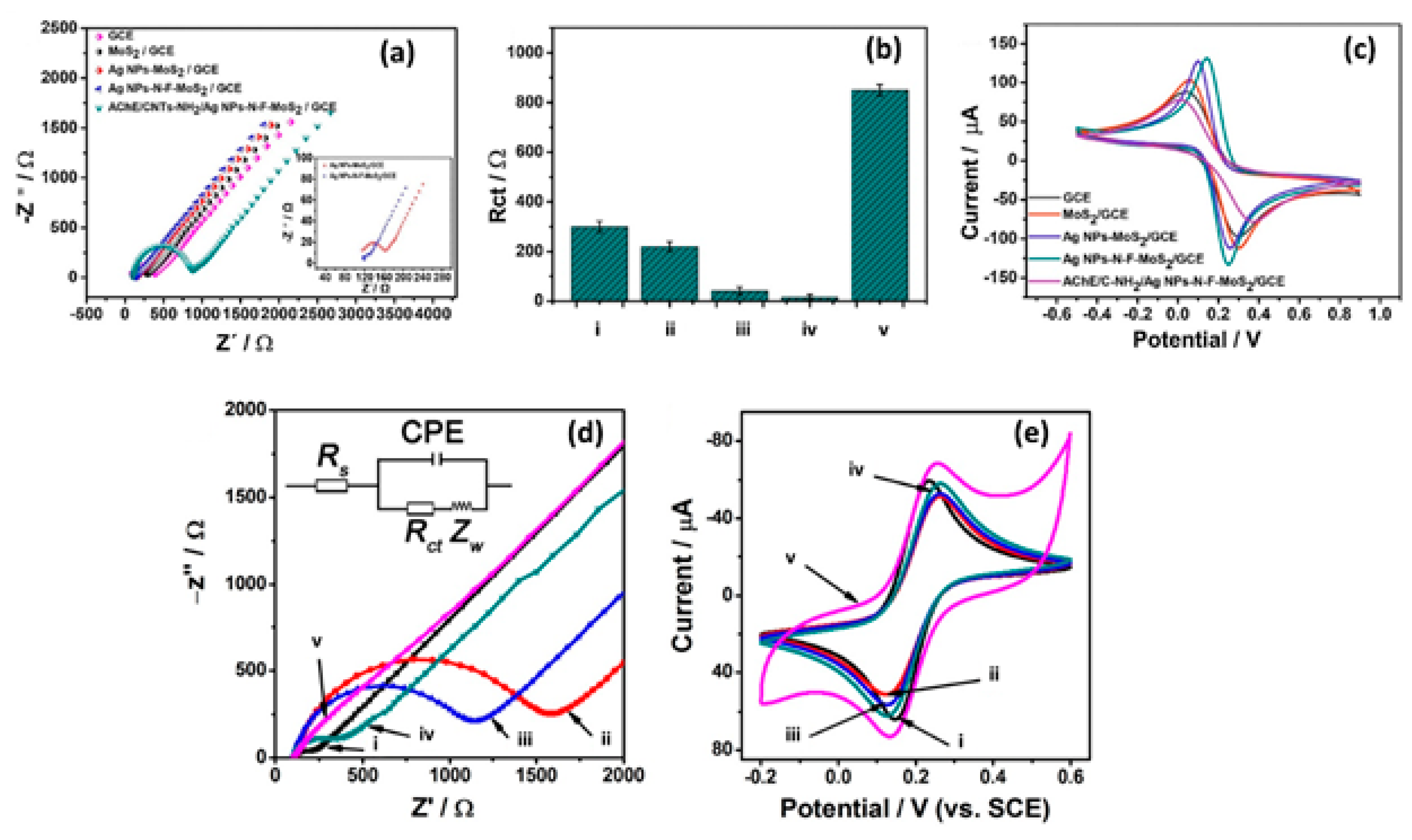
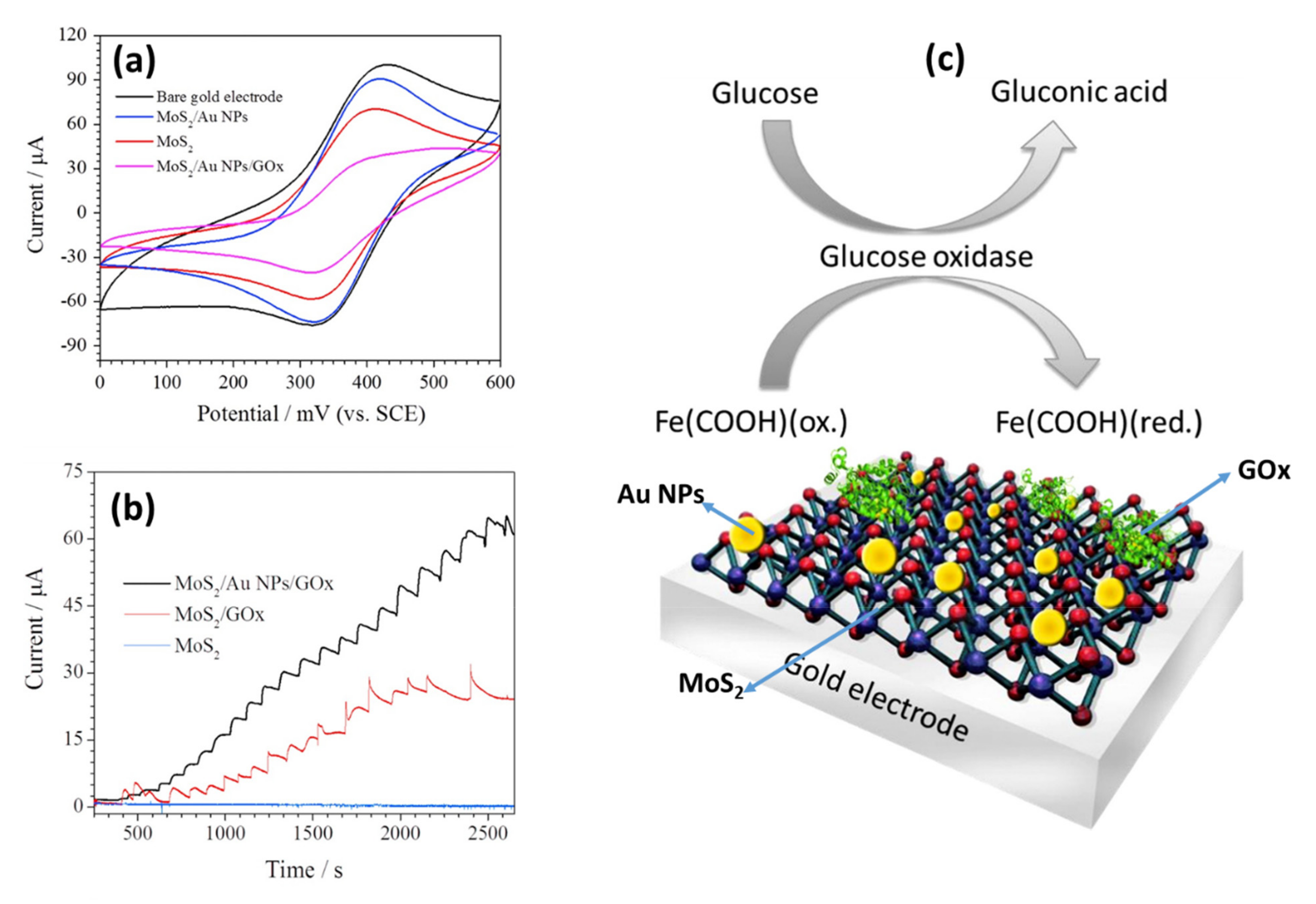
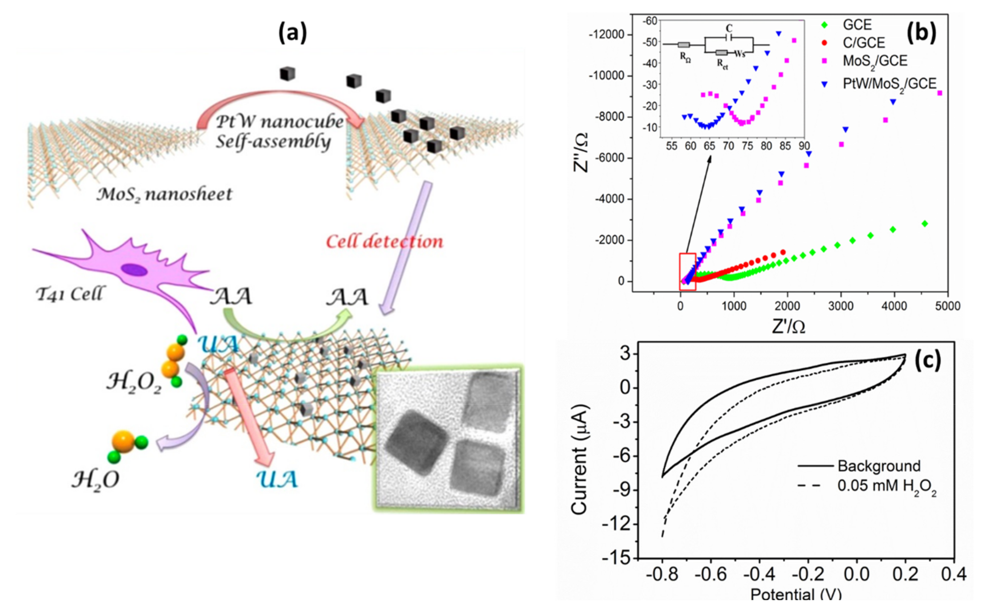
5.1. Electrochemical Biosensors

Recently, significant progress has been made in the development of electrochemical sensors and their application in point-of-care diagnostics, environmental studies, food safety, drug screening, and security. Electrochemical sensing has proven to be a simple analytical technique for detection of various chemicals and biological molecules due to intrinsic advantages, such as high sensitivity and selectivity, real-time measurements, low-cost instrumentation, and the potential for miniaturized and portable devices. A standard electrochemical sensor has three components, namely, a recognition component that specifically binds the target analyte, a transducer where specific reactions occur and a signal is produced, and an electronic component that converts the obtained signal to a response [195]. The operating mechanism of an electrochemical sensor involves the interaction of the target analyte with the electrode surface coated with a catalyst, and producing the desired change in the signal as a result of a redox reaction [196]. The reaction results in electrical, thermal, or optical output signals that can be used to investigate the nature of the analyte species [197]. The active sensing materials could be biological or chemical compounds that function as catalysts for sensing specific analytes [197]. Sensitivity and selectivity are essential variables in electrochemical sensors. Thus, the surface modifications of electrodes by immobilization of specific chemical or biological recognition elements is an efficient technique used for obtaining optimal binding of the target analyte. Commonly used biorecognition elements include enzymes [69], antibodies and antigens [70,96], aptamers [95], proteins [198], etc., for high catalytic activity and excellent selectivity of the target analytes. Even so, the resulting signal from biorecognition molecules is not strong enough to achieve the ultra-sensitive detection of biomolecules required for early and rapid diagnosis of diseases [199]. Biorecognition molecules have therefore been integrated into nanomaterials to address this limitation, and to significantly improve the overall performance of the biosensor [200]. The 2D MoS2 nanosheets are among the nanomaterials that have become incredibly popular for sensing applications. They have been reported to be good electrode materials for electrochemical sensing; hence, there is an increasing number of publications addressing their integration into sensors [69,108]. Although 2D MoS2 has low electrical conductivity compared to graphene due to its large band gap limiting its use as a pristine material, 2D MoS2 has tunable properties that depend on the crystal structure, nanosheet size, and surface defects [146,148,161], as already discussed in detail earlier. This gives researchers the opportunity to explore the electrocatalytic properties of non-functionalized 2D MoS2 for the detection of biological molecules. In a study presented by Wang et al. [201], an electrochemical sensor based on non-functionalized MoS2 nanosheets was fabricated for detection of DNA. The reported results indicated that the bulk MoS2 had no electrocatalytic effect due to the low electronic conductivity that resulted from the poor interlayer electron transport. However, the exfoliated MoS2 nanosheets showed increased electrochemical activity with a decreased change in potential (∆Ep). The enhanced electrocatalytic activity of MoS2 nanosheets was discovered to be due to the anisotropic layered structure of MoS2 nanosheets, whose electronic structures and electrochemical activities are directly influenced by the layer thicknesses of the nanosheets [201].
Moreover, Sha and co-workers explored the electrocatalytic properties of hydrothermally-grown non-functionalized MoS2 nanosheets on aluminum foil toward non-enzymatic detection of uric acid in human urine [202]. The group demonstrated a two-step successful growth of a few layered ( < 4 layers) MoS2 nanosheets with a high ratio of 1T phase MoS2 than 2H phase MoS2. This was not a typical sensor, in the sense that the aluminum foil was used as a sensor substrate, which contributed to the excellent selectivity and reproducibility, fast response time, and low limit of detection. The impressive sensing ability also resulted from a high proportion of the metallic 1T phase MoS2, which provided excellent conductivity, rapid electron transfer kinetics, and more exposed catalytic active sites arising from a significant number of surface defects [202]. The results of these two sensors are based on phenomena that describe the direct structure-dependent properties of MoS2. Changes in the interlayer coupling, the degree of quantum confinement, and symmetry elements result in major variations in the 2D MoS2 electronic structure compared to bulk [9,144,145,146]. The reduction in size of MoS2 offers abundant exposed edges, kinks, and corner atoms that induce additional chemical effects [149,190]. Moreover, the quantum size effects lead to changes in the valence band and the oxidation potential, thereby enabling catalytic activities not possible with the bulk band structure [149].
Primarily, due to its fundamental drawbacks, non-functionalized 2D MoS2 is rarely used as both an electrocatalyst to interact directly with the target analyte and as an electron transfer mediator to enhance the signal simply because its surface area is substantially reduced. Nevertheless, the synthesis or incorporation of 2D MoS2 into other nanomaterials to form nanocomposites could efficiently preserve its large specific surface area and improve its catalytic activity [203]. The large surface area of 2D MoS2 offers effective surface functionalization and creates new possibilities for practical applications. Functionalizing 2D MoS2 nanosheets with metal and metal oxide NSs can effectively exploit distinct properties of both materials through a synergistic effect between metal-based NSs and MoS2 nanosheets, which could result in greater electrocatalytic efficiency, conductivity, and prevent restacking of nanosheets. For instance, Au NPs were post-immobilized on MoS2 nanosheets for electrochemical detection of glucose [69]. Electrochemical techniques, such as CV and EIS, were utilized to study the interfacial electrochemical properties resulting from the synergistic effect between Au NPs and MoS2 nanosheets. The CV results (Figure 8a) showed that MoS2 was able to promote fast electron transfer kinetics; however, a dramatic increase in the current response was observed when the electrode surface was modified with the MoS2-Au nanocomposite [69]. This indicates that structuring of the Au NP created a higher electroactive surface area and provided a more conductive interlayer for the transfer of electrons. In an effort to further demonstrate the efficiency of MoS2-Au nanocomposite, glucose oxidase (GOx) was immobilized on the MoS2 and MoS2-Au nanocomposites to achieve optimal binding of glucose and to study its electrocatalytic oxidation. According to the amperometric measurements (Figure 8b), an electrocatalytic response was achieved with both MoS2-GOx and MoS2-Au-GOx, and a steady-state current was recorded within 5 and 3 s, respectively [69]. Generally, glucose oxidase catalyzes the oxidation of glucose to produce gluconic acid and hydrogen peroxide in the presence of oxygen, as shown in Figure 8c. During this conversion, two protons and two electrons transfer from glucose to the flavin moiety of GOx [204]. While both electrodes were able to catalyze glucose, MoS2-Au-GOx provided good electrocatalytic performance, high sensitivity, and a low detection limit, thereby proving that the Au NPs on the surface of MoS2 enhanced the conductivity, improved the surface area for effective GOx immobilization, and facilitated rapid electron transfer. Although GOx is electroactive and has active sites that can be electrochemically reduced by direct electron transfer [205], it has disadvantages, such as thermal and chemical instability, critical operating conditions, such as optimum temperature, humidity and pH, low sensitivity, and reproducibility [35,93]. Controlling the interactions of enzymes with the substrate to improve electron transfer processes remains a challenge that causes a substantial loss of GOx activity, leading to poor overall performance of the sensor. Therefore, other researchers saw an opportunity to explore various 2D MoS2/metal-NS composites (Ni-MoS2 [35], CuO-MoS2 [82], Cu-MoS2 [85], Au-Pd/MoS2 [89], Cu2O-MoS2 [93], NiO-MoS2 [103], NiCo2O4-MoS2 [108], and MoS2-PPY-Au [206]) as electrode materials to construct non-enzymatic sensors due to their extraordinary electrocatalytic activities, excellent conductivity, and large surface areas. The experimental results revealed that the performances of all these 2D MoS2/metal-NS composites were remarkable, as shown in Table 2. These sensors demonstrated excellent electrocatalytic capabilities to oxidize glucose without the enzyme, with high sensitivity and low detection limits.
In another study, Zhu and co-workers functionalized MoS2 with PtW nanocubes for detection of H2O2 released from breast cancer 4T1 cells [94] (Figure 9a). The study revealed that the functionalization of MoS2 with PtW nanocubes to form a composite improved the selective interaction of hydrogen peroxide (H2O2) with the sensing film, and further increased the sensitivity and selectivity of a sensor. The experimental results obtained from EIS and CV (Figure 9b,c) showed that the MoS2-PtW nanocomposite could catalyze H2O2 and reduce the charge transfer resistance, enabling rapid electron transfer kinetics compared to MoS2 alone. The group reported that the good electrocatalytic performance could be due to the fact that the integration of PtW nanocubes on the surface of MoS2 opened interlayer spacing in the hybrid structure, providing rich reactive sites and favorable surface permeabilities, further enhancing sensitivity during sensing processes [94]. In this sense, it is worth mentioning that the morphological structure of the PtW also played a significant role in electrocatalytic efficacy of the nanocomposite. Although the group did not study the effects of structural morphology, size, and shape toward the electrocatalytic properties of NSs, studies have shown that the structural morphologies of nanomaterials on the electrode surfaces have the potential to enhance the biomolecule sensing efficiency in terms of (i) electron transport durability, (ii) molecular adsorption capability, (iii) suitable lodging of targeted biomolecule [205,207].
Electrode modification with 2D-MoS2/metal-NSs composites has shown great potential in electrochemical biosensors. Current studies have demonstrated the ability of 2D-MoS2/metal-NSs composites to provide a convenient platform for the immobilization of biorecognition molecules and further enhance the electron transfer, resulting in faster reaction times and higher sensitivity [200]. It is therefore considered that nanocomposites based on 2D-MoS2/metal-NSs hold significant potential as active electrocatalysts for the development of highly sensitive and selective electrochemical sensors. Table 2 shows the performance of electrochemical biosensors based on 2D-MoS2/metal-NSs composites with and without biorecognition molecules for detection of various analytes.

5.2. Electrochemical Immunosensors

Electrochemical immunosensors (EIs) have received considerable attention due to their high sensitivity, low cost, simple instrumentation and operation, and inherent miniaturization [214,215,216]. They show great potential in the next-generation of point-of-care (POC) diagnostics for early detection and monitoring of diseases. An electrochemical immunosensor is a type of biosensor used to detect the specific antigen–antibody recognition; it quantitatively measures the resulting electrochemical signal [70,107]. The basic immunosensor concept is to load the antibody onto the electrode surface. Following the specific antigen–antibody binding, the electron transfer rate between the electrode surface and the solution interface changes, resulting in the production of membrane potential and change of the current response, which directly reflects the concentration of the targeted antigen [107]. This type of immunoassay sandwich is a common format of an immunosensor. Countless efforts have been made into the advancements of EIs to improve performance by achieving high sensitivity. This includes the use of different nanomaterials, such as layered nanomaterials [217], metal and metal oxides NSs [218,219], and carbon-based nanomaterials [123] to amplify the EI signals. Due to excellent catalytic activity and biocompatibility, MoS2 functionalized with metal or metal oxide NSs has recently been introduced among nanocomposites used in the construction of immunosensors. Tan et al. [90] developed a label-free PtPd-MoS2 nanocomposite-based immunosensor (Figure 10a) for quantitative detection of the hepatitis B surface antigen (HBs Ag). Under optimal conditions, the PtPd-MoS2-based electrochemical sensor was able to attain a lower detection limit of 10.2 fg/mL compared to the colorimetric method (3.3 pg/mL). This excellent detection limit was attributed to the synergistic effect between the two nanomaterials, which resulted in an increased substrate reaction rate, electron transfer efficiency, and enhanced sensitivity. The chronoamperometry method was used to characterize the catalytic efficiency of the presented nanomaterials. The findings (Figure 10b) indicated that the PtPd-MoS2 nanocomposite (curve iii) produced a higher current response than MoS2 (curve i) and PtPd nanocubes (curve ii) due to the distinctive cubic stacking structure of PtPd on the large surface area of MoS2. Most importantly, the group noted that the cubic structure of PtPd offered more active sites than nanospheres, and improved the biocompatibility and the easy binding of antibodies by Pt–N bonds and Pd–N bonds, which more likely increased the amount of the bound antibody. To further demonstrate the excellent sensitivity of the prepared electrochemical immunosensors, the group used the PtPd-MoS2 nanocomposite in colorimetric sensors for comparison. They found that in the colorimetric sensor, the immune composite film formed on the sensing surface as the antigen concentration increased and actively inhibited the diffusion pathway of the substrate to the signal interface, resulting in a reduced current response. On the contrary, the PtPd-MoS2 nanocomposite exhibited excellent electrocatalytic behavior in differential pulse voltammetry (DPV) response (Figure 10c) due to the effective electron transfer kinetics [96]. The sensor was able to capture biomolecules efficiently and amplify current signals; it showed good specificity, reproducibility, and stability.
The application of enzyme amplification has also been an effective way to further enhance the detection efficiency of nanomaterials. With the aim of improving detection accuracy of electrochemical immunosensors, Su and co-workers [220] developed an enzyme-assisted signal amplification approach for the detection of carcinoembryonic antigen (CEA) using the benefits of the MoS2-Au NPs composite and the catalytic effect of biological enzymes, as shown in Figure 11a. They immobilized horseradish peroxidase (HRP)-labeled carcinoembryonic monoclonal antibody (anti-CEA) and HRP on the MoS2-Au surface to create a MoS2-based sensing film that could greatly enhance the electrochemical response. As expected, the experimental results obtained from CV and EIS (Figure 11b,c) confirmed that the MoS2-Au nanocomposite had excellent electron transfer kinetics and reduced charge transfer resistance prior to enzyme immobilization. A decrease in the current response after modification with anti-CEA and HRP suggests an effective immobilization of the enzymes on the surface of MoS2-Au. It is commonly known that enzymes frequently inhibit the transfer of electrons and, therefore, an electroactive mediator (e.g., nanomaterials) is often required to promote the transfer of electrons. With that said, the HRP/HRP-anti-CEA/MoS2-AuNPs-modified electrodes showed the best electrocatalytic performance compared to other modified electrodes when they reacted with 1 ng mL−1 CEA in the absence (curve i) and presence (curve ii) of hydrogen peroxide H2O2 (Figure 11d–g). The excellent electrochemical response of the proposed sensors (HRP/HRP-anti-CEA/MoS2-AuNPs) was based on the perception that MoS2-Au nanocomposites improved the conductivity and increased the loading of anti-CEA and HRP-anti-CEA due to the large surface area. Moreover, The HRP labeled anti-CEA catalyzed the o-phenylenediamine (o-PD) in the presence of H2O2 and further enhanced the detection signal. Ultimately, the HRP blocked the nonspecific adsorption of the immunosensor, which multiplied the electrochemical signal due to an enzymatical catalytic reaction [220]. As a result, the fabricated immunosensor displayed high sensitivity and selectivity, good stability, and a low detection limit of 1.2 fg mL−1. It must be noted that, despite extensive handling and complexity of the enzymes, many researchers still find them to be ideal biorecognition molecules to improve the electrocatalytic behaviors of nano-based electrochemical sensors. Table 3 summarizes the performance of EIs based on 2D-MoS2/metal-NSs composites.

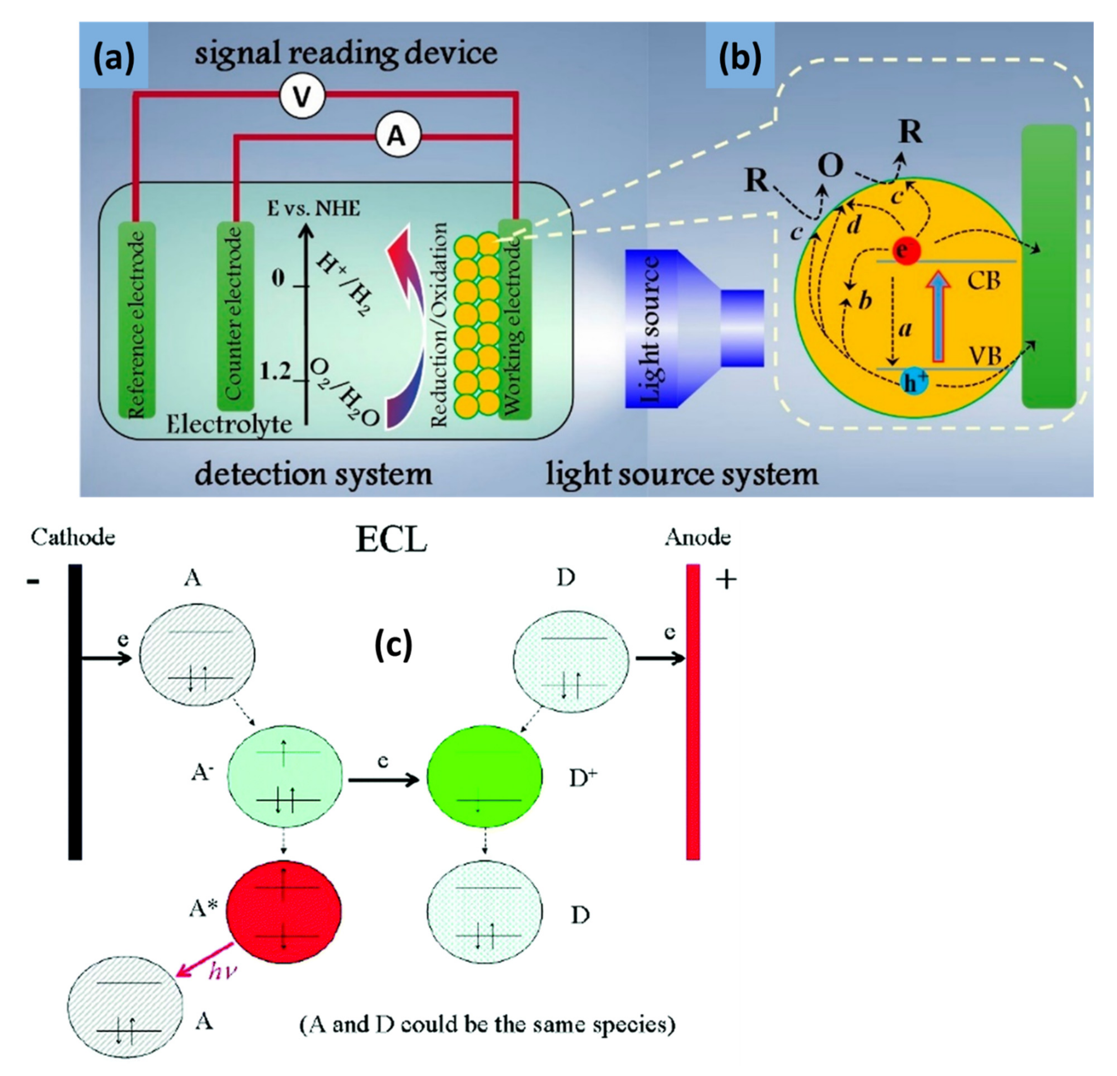
5.3. Photoelectrochemical Sensors

PEC sensing has experienced rapid growth as an important branch of electrochemical detection. PEC analysis, due to high sensitivity, fast detection, and low background current, has been wildly adopted in bioanalytical chemistry as a newly emerging and continuously developing analytical method [176]. The standard PEC sensor uses light as an excitation source and photocurrent as a signal identifier. Photoactive materials are immobilized on the electrode surface as a photo-to-current converter to generate photocurrent signals under light irradiation. The photo-to-current conversion results from the electron excitation and subsequent charge transfer of a material after absorbing photons [172,226]. The total separation of the source of excitation (light) and detection signal (photocurrent) enables this method to have the advantages of a low background signal and high sensitivity to recognize target analytes in complex samples as opposed to traditional optical methods [174,227]. Photoactive materials play critical roles in PEC systems; The PEC sensor output depends on the properties of these materials since they can influence the sensitivity and selectivity of the PEC sensor. Different photoactive materials, such as metal-based NPs [227,228], quantum dots (QDs) [229], carbon-based nanomaterials [230], layered nanomaterials [176], etc., have been studied in PEC application to fulfil specific demands. Furthermore, biological molecules, such as enzymes, antibodies, nucleic acids, etc., are also important for specific recognition in PEC biosensors and immunosensors. Amongst the photoactive materials, 2D MoS2 is the latest emerging material for use in PEC biosensors and immunosensors because of its special optical properties. Hun et al. [176] developed a PEC sensor based on a single-layer MoS2 nanosheet for detection of dopamine (DA). The fabricated sensor showed an incredible photocurrent response, which demonstrated that PEC activity was enhanced by the single-layer MoS2. That is because single-layer MoS2 exhibits exceptional semiconducting electronic properties as well as a good photocurrent with a sensitive photoresponse compared to multilayer MoS2. The photocurrent proportionally increased with the concentration of DA in the range of 0.01 nM to 10 µM with a detection limit of 0.0023 nM. Even though different photoactive materials are available for the fabrication of PEC sensors, due to the limitations of a single material, it is difficult to achieve the ever-increasing demands for detection. However, any drawbacks of the pristine photoactive material, such as MoS2, can be resolved by flexible nanocomposites with the tailor-made structure and composition [173]. Additionally, certain biological molecules, such as cells and DNA, can produce photocurrents by themselves. Thus, the interactions between these biomolecules and other photoactive materials can be examined through the change of photocurrents [172]. In general, PEC biosensing or immunosensing refers to the effect on the photocurrent signal of the interaction between the biorecognition molecule and the analyte, which involves the charge and energy transfer of the PEC reaction between the electron donor/acceptor and the photoactive material during light irradiation [174]. Liu et al. [106] fabricated a PEC biosensor by immobilizing glucose oxidase on an MoS2 nanosheet-TiO2 nanorod composite modified indium tin oxide (ITO) electrode for detection of glucose (Figure 12a). The PEC properties of nanomaterials were studied by irradiating the modified electrodes with visible incident light. According to the photocurrent results (Figure 12b), both pristine MoS2 (curve i) and TiO2 (curve ii) had small photocurrent responses. The small photocurrent response of non-functionalized MoS2 might be attributed to poor excitation capability caused by the material’s band gap. As expected, after functionalization with TiO2 nanorods, the MoS2-TiO2 nanocomposite (curve iii) exhibited a photocurrent that was 4.8 times greater than that of pristine MoS2 and TiO2. It is widely understood that the interfacial interaction between MoS2 nanosheets and TiO2 nanorods and the matched energy band levels improved the visible light absorption and increased the charge separation [179]. A sudden decrease in photocurrent response was observed after immobilization of the enzyme on the MoS2-TiO2 nanocomposite (curve iv). This decrease was due to the steric obstruction of the enzyme molecules, which prevented the transport of photogenerated electrons to the electrode surface and, thus, increased their recombinations with the holes [106]. Besides the adverse effect on the photocurrent response—GOx facilitated the catalytic oxidation of glucose and improved the sensitivity the PEC sensor. The biocatalytic results obtained from CV (Figure 12c–e) indicated that the excitation of visible light enhanced the current response of the Gox-modified electrodes towards glucose, suggesting that the catalytic behavior of GOx to glucose under illumination improved the photo-electrocatalytic activity of the sensor.
The proposed mechanism (Figure 12a) of the sensor was that the lower conduction band (CB) energy level of bulk or multi-layer MoS2 (1.2 eV), as shown by the dash line, would prohibit the electron injection from MoS2 CB to the higher CB of TiO2. However, due to the quantum confinement effect, the energy band gap of MoS2 (1.8 eV) increases with the decreasing number of layers. Moreover, according to theoretical calculations, the thickness of MoS2 would mainly influence the conductive band (CB) level of MoS2, and not affect the valence band level (VB). Therefore, the CB energy level of few-layer MoS2 becomes higher than that of TiO2 (solid-line arrows), resulting in the matched energy bands between MoS2 and TiO2 and an electron injection from MoS2 to TiO2 [106,179]. When GOx is immobilized, it catalyzes the oxidization of glucose to gluconolactone, while O2 simultaneously reduces to H2O2 [231]. The radiation of visible-light causes the photogenerated electrons from the VB of MoS2 to jump to the CB of MoS2; this electron is transmitted to the CB of TiO2 and is eventually attracted to the positive ITO electrode, leaving the holes in the VB of MoS2. As a result, the photogenerated electron–hole pairs are effectively separated and the visible-light photoactivity is enhanced. Simultaneously, the photogenerated holes left in the VB of MoS2 are consumed by H2O2, which hinders the recombination of photogenerated charges and, therefore, increases the photo-current [106,179].
Inspired by the good photocatalytic properties of the MoS2-TiO2 nanocomposite, Liu and co-workers also developed a PEC aptasensor based on the TiO2-MoS2-AuNPs composite for detection of kanamycin [90]. The incorporation of Au NPs to MoS2-TiO2 was intended to further enhance the photocurrent response of the sensor. The group noticed that due to the surface plasmon resonance effect of Au NPs, the NPs would directly convert the incident visible light into electrical energy by injecting photogenerated electrons into the MoS2 conduction band, which would then increase the efficiency of the photoelectric conversion. As expected, the TiO2-MoS2-AuNPs composite showed an approximate two-fold increase in the photocurrent compared to the MoS2-TiO2-modified electrode. A similar trend was observed in comparison with Figure 12b (curve iv), in that, following the immobilization of the biorecognition element (aptamer), the photocurrent response of the TiO2-MoS2-Au nanocomposite decreased significantly. This was due to the steric hindrance of the biological molecules, which prevented the transport of the photogenerated electrons from moving to the electrode surface. Interestingly, under optimal conditions, the specific interaction between the aptamer and kanamycin resulted in an increase in the photocurrent response due to the oxidation of kanamycin by the photogenerated holes, which improved the overall performance of the sensor [90].
In another study, Han et al. [232] utilized the good PEC properties of the MoS2-ZnO nanocomposite to construct the PEC sensor for the detection of the propyl gallate (PG) antioxidant without the biorecognition element. The photoelectrochemical performance of the MoS2-ZnO heterostructure was studied by irradiating the modified electrodes with 470 nm of visible light. The obtained photocurrent results (Figure 13a) indicated that MoS2-ZnO had a higher photocurrent response in the PBS solution as compared to pristine n-type ZnO and p-type MoS2 nanomaterials. A similar trend was observed upon addition of 12.43 μmol L−1 PG; MoS2-ZnO showed a drastic increase in the photocurrent response compared to pristine ZnO and MoS2. The group indicated that the incorporation of ZnO into MoS2 tends to form a p−n heterojunction for efficient carrier separation and light absorption, leading to a high photocurrent response. Furthermore, the photocurrent response of the MoS2-ZnO-modified electrode to a range of PG concentrations was analyzed and the results demonstrated a favorable linear relationship between the wide range of PG concentrations (0.1249–1643 μmol L−1) and the photocurrent responses, as shown in Figure 13b. The sensor displayed outstanding PG detection capability with undeniably higher sensitivity and selectivity, good stability, and a wider linear range. According to the proposed mechanism (Figure 13c), the three adjacent PG hydroxyl groups bind to the Zn(II) surface site of ZnO to form a chelate structure, resulting in a higher concentration of PG near the MoS2-ZnO photocatalyst. Thereafter, the electrons and holes of MoS2-ZnO separate and generate a photocurrent under light irradiation. The electrons would then be transferred from MoS2 to ZnO and, in response, the holes formed by MoS2 would efficiently oxidize PG. The proper conduction band formed in MoS2-ZnO nanocomposites effectively enhances the transfer of electrons from ZnO to the ITO electrode, which not only decreases the recombination rate between the electron and the hole, but also enhances the sensitivity of the MoS2-ZnO-based PEC sensor. Table 4 summarizes the performances of various PEC sensors based on 2D-MoS2/metal-NSs composites [232].

5.4. Electrochemiluminescence Sensors

ECL detection is commonly used in the various applications for biosensors. This technique combines the advantages of electrochemistry and chemiluminescence in resolving single sensing limitations, making it more desirable for precise detection and enhancement of a sensor’s sensitivity and specificity. ECL refers to the light emission from an excited state produced by the electron transfer reaction between species at electrode surfaces following electrochemical reactions [236]. ECL detection consists of measuring photon output and, thus, the light intensity emitted in the solution during an electrochemical reaction. The light intensity is therefore directly proportional to the concentration of one or more of the reactants involved in the electrochemical reaction [237]. ECL has many advantages over photoluminescence, such as simplicity, high sensitivity, and rapidity response, and does not require the use of an external light source, leading to a high luminescent purity and a low optical background noise [236,238]. Furthermore, the ECL emission light can be initiated and controlled with high reproducibility and accuracy by alternating the applied potential [236,239]. Unfortunately, one of the drawbacks of the ECL method is the possibility of electrode fouling, which can result in poor reproducibility. While this could sometimes be a concern in the presence of complex samples, this effect can be avoided by frequent electrochemical cleaning of the electrodes. Moreover, new electrode materials that are less prone to fouling, such as boron-doped diamond and disposable screen-printed electrodes, have been introduced and have become more popular [240]. The continuous development of nanomaterials offers new opportunities for conventional ECL research, mainly owing to their large surface area, abundant active sites, and distinctive optical properties. Nanomaterials with good electron transfer capabilities, such as 2D nanomaterials [241], quantum dots [242], and metal nanoparticles [243], have also been implemented to improve the efficiency of ECL sensors. Among these nanomaterials, the use of 2D MoS2 in ECL sensors is not so prominent. This is attributable to the fact that 2D MoS2 is not capable of generating electrochemiluminescence; however, it serves other functions, such as acting as a robust substrate or amplifying the signal [244]. MoS2 can also be used as a carrier for other nanomaterials with structural and compositional benefits to improve the ECL performance.
In that context, Zhang et al. [81] fabricated a sandwich ECL immunosensor for the detection of alpha fetal protein (AFP) based on MoS2-PEI-Au nanocomposites. As shown in Figure 14a, polyethylene (PEI) was first introduced to the surface of the MoS2 nanosheets to serve as a binding agent that can absorb the negatively charged Au NPs by electrostatic attraction. The formed MoS2-PEI-Au nanocomposite was used to capture the Ab1 and Au@BSA-luminol as a signal probe to immobilize Ab2, respectively (Figure 14b). In order to confirm the efficiency of the Au@BSA-luminol signal probe, the group studied the ECL behavior of the immunosensor before and after the immobilization of Au@BSA-luminol (Figure 14c) on the surface of MoS2-PEI-Au-Ab1 in the presence of H2O2 and AFP. The obtained result indicated that the MoS2-PEI-Au modified electrode could produce the ECL signal only after the presence of Au@BSA-luminol-Ab2, which demonstrated the efficiency of the bioconjugate as a luminescence reagent. In addition, the substantial enhancement on the ECL-sensing signal was due to the catalytic efficiency of MoS2 nanosheets, which could decompose H2O2 to increase the ECL intensity of luminol, and the excellent electrical conductivity of Au NPs, which facilitated the electron transfer and further enhanced the sensitivity of the ECL immunosensor. Under optimal conditions, a fabricated sandwiched immunoassay sensor was used to detect a series of AFP concentrations in 0.01 M PBS. The ECL intensity was found to increase simultaneously with an increase in concentration of AFP, as shown in Figure 14d. The target AFP molecules were being sandwich, captured between the primary antibody and the Au@BSA-luminol-Ab2 bioconjugate by means of a immune-specific reaction, leading to an enhanced detectable ECL signal. Based on the low detection limit obtained, the high sensitivity and increased intensity of the ECL signals, a rapid and sensitive quantitative detection of AFP was therefore successfully attained. Table 5 summarizes the performances of a few ECL sensors that have been reported based on 2D-MoS2/metal-NSs composites.
Focusing on the application of 2D MoS2-metal NS composites on various electrochemical sensors, it can be inferred that 2D MoS2 represents a new class of highly electroactive materials. The large surface areas of 2D MoS2 nanosheets enable surface functionalization with a variety of nanomaterials, providing new opportunities for 2D material-based functional devices. The effective support structure of MoS2 nanosheets allows for a good distribution of metal-based NSs, resulting in a synergistic effect that enhances catalytic efficiency and conductivity over a pristine MoS2. Furthermore, 2D-MoS2/metal-NS composites provide a convenient platform for the immobilization of biorecognition molecules and enhance electron transfer, resulting in faster reaction times as well as increased sensitivity and selectivity. Therefore, 2D MoS2-NSs composites are thought to have considerable potential as effective electrocatalysts for the production of highly responsive electrochemical sensors with low limits of detection.

6. Challenges, Limitations, and Future Outlooks

The fabrications of 2D MoS2 nanosheets as well as their use in electrochemical sensors have advanced significantly in recent years. However, uniform growth of high quality 2D MoS2 nanosheets in large-scale production remains a challenge. It is generally acceptable that controlling the number of layers, size, purity, stoichiometry, and phases of 2D MoS2 is not only enigmatic but also a demanding task. Although liquid–phase exfoliation is ideal for high scalability and crystallinity, a low yield of monolayers is inevitable, while the size distribution is rather wide. Moreover, environmental stability of 2D MoS2 poses some significant challenges. At ambient temperatures, pristine MoS2 nanosheets degrade gradually due to surface contamination and significant oxygen adsorption in an air environment [19,20]. More developments and optimization of the MoS2 nanosheet preparation methods are necessary to improve the quality of the material. Furthermore, emphasis should be placed on the development of improved surface functionalization methods capable of providing good control over the size and distribution of metal-based NSs on MoS2. It is fundamentally important to achieve a homogeneous dispersion of non-agglomerated NPs in the nanocomposite matrix using both in situ and ex situ functionalization methods. The uniform distribution of NPs degrades the properties of the nanocomposite. A high loading of NPs on the surface of MoS2 was also discovered to cause decay [69].
Metal-based NSs have shown great capability to improve the electrical, optical, and catalytic properties of 2D MoS2 in response to various redox processes. It is a known fact that metal-based NSs provide more active sites on the surface of the MoS2 nanosheet to improve electrocatalytic activity and electron transfer kinetics for the detection of various target analytes. However, because a MoS2-metal-based nanocomposite cannot electrocatalyze most biological molecules, the use of biological recognition elements, such as enzymes, aptamers, and antigen-antibodies as bioreceptors, remains prevalent. Extensive research on the mechanism of functionalization and its effect on the electronic band structures of MoS2 is lacking. As a result, failing to understand the interactions between MoS2 nanosheets and NPs limits the ability to further improve these nanocomposites for use in electrochemical sensors. In this sense, a thorough understanding of the catalytic mechanisms and structure configurations of MoS2 active sites can provide valuable guidance in resolving existing issues, potentially eliminating the need for biological recognition elements. Furthermore, stability of MoS2-metal-based nanocomposites was shown to be one of the limiting factors for improved catalytic efficiency. Most sensors showed a decrease in performance over a period of 4 weeks, indicating long-term stability issues of the MoS2-metal-based nanocomposites [96,198,212,223]. This is a problem because sensor stability and durability are critical requirements in commercial and industrial settings. Therefore, core advancements should be on developing various synthesis methods for 2D MoS2 nanocomposites that exhibit outstanding stability. Nonetheless, given recent advancements in the fabrication of MoS2-based sensors and biosensors, we anticipate extensive use of 2D-MoS2/metal-NSs composites for developing dimension-tailored devices, such as wearable sensors, for a variety of applications in the near future.

7. Conclusions

We highlighted some main features of MoS2 nanosheets when they are exfoliated into single or a few layers, the effects on properties when functionalized with metal and metal oxide NSs, and recent advances in electrochemical sensors based on 2D-MoS2/metal-NSs composites. Reducing the number of layers results in a gradual shift in the indirect band gap to a large direct band gap in single layers, which turns the material into a 2D semiconductor. Multiple methods have been suggested for synthesizing 2D MoS2; these methods can also be used to tune the 2D MoS2 electronic band structure. Methods (e.g., the Li intercalation and CVD) were found to alter the optical and electrical properties of material by simply manipulating the experimental conditions. The Li intercalation of MoS2 results in a structural transformation of MoS2 from phase 2H to phase 1T, as well as a transition from the semiconductor to metallic 2D MoS2 nanosheet. The interesting thing to note is, owing to the nature of the exfoliation process, many imperfections may occur on the material surface. Control of high quality, large surface areas, and a uniform 2D MoS2 are therefore necessary in order to further produce desirable nanosheets and to strongly understand the material’s surface chemistry. While various methods for preparing 2D MoS2 nanosheets have been developed, obtaining the perfect 2D MoS2 fitting the above requirements remains a challenge. Even so, 2D MoS2 and other layered materials still play important roles in the general application of sensors. On the other hand, functionalizing or doping MoS2 nanosheets would adjust or add the required properties to the material, which can be used in the fabrication of sensors. Integrating metal-based NSs on MoS2 nanosheets can effectively exploit the distinct qualities of both materials. This can be accomplished by ex situ or in situ functionalization. While it has been confirmed that MoS2 simply forms nanocomposites with metal and metal oxide NSs, achieving a homogeneous dispersion of non-agglomerated nanoparticles within the nanocomposite matrix remains a challenge. We noted that the method of preparation, functionalization, and layer thickness play important roles in the electrical, optical, and catalytic properties of the material. Control over these properties during production is therefore essential for the ultimate application regardless of the method of synthesis and functionalization. Recently, various sensors based on 2D-MoS2/metal-NSs composites have been developed, from field effect transistors (FET) to electrochemical sensors. Emerging research and publications have shown that 2D-MoS2/metal-NSs composites serve as good platforms for sensing. The nanocomposites offer a new range of highly-electroactive materials and may further advance to better the electrochemical sensing performance.

Author Contributions

The manuscript was written through contributions of all authors. N.M.: Investigation, Writing—original draft, Methodology. L.S.: Conceptualisation, Supervision, Project administration, Funding acquisition, Formal analysis, Writing—review & editing. S.S.R.: Conceptualisation, Supervision, Project administration, Funding acquisition, Formal analysis, Writing—review & editing. All authors have read and agreed to the published version of the manuscript.

Funding

This research received no external funding.

Institutional Review Board Statement

Not applicable.

Informed Consent Statement

Not applicable.

Data Availability Statement

Not applicable.

Acknowledgments

The authors wish to acknowledge the Department of Science and Innovation (DSI)—South Africa, DSI/Mintek, Nanotechnology Innovation Centre (NIC) for financial support. The authors also acknowledge financial support from the Council for Scientific and Industrial Research (CSIR)—South Africa, University of Johannesburg (UJ) and University of Venda (UNIVEN). Lastly, the authors wish to acknowledge NIPMO (The National Intellectual Property Management Office—South Africa and Centre for High Performance Computing (HPC) for support.

Conflicts of Interest

The authors declare no conflict of interest.

References

  1. Bhimanapati, G.R.; Lin, Z.; Meunier, V.; Jung, Y.; Cha, J.; Das, S.; Xiao, D.; Son, Y.; Strano, M.S.; Cooper, V.R.; et al. Recent Advances in Two-Dimensional Materials beyond Graphene. ACS Nano 2015, 9, 11509–11539. [Google Scholar] [CrossRef] [PubMed]
  2. Butler, S.Z.; Hollen, S.M.; Cao, L.; Cui, Y.; Gupta, J.A.; Gutiérrez, H.R.; Heinz, T.F.; Hong, S.S.; Huang, J.; Ismach, A.F.; et al. Progress, Challenges, and Opportunities in Two-Dimensional Materials Beyond Graphene. ACS Nano 2013, 7, 2898–2926. [Google Scholar] [CrossRef] [PubMed]
  3. Xu, M.; Liang, T.; Shi, M.; Chen, H. Graphene-Like Two-Dimensional Materials. Chem. Rev. 2013, 113, 3766–3798. [Google Scholar] [CrossRef] [PubMed]
  4. Hu, G.; Kang, J.; Ng, L.W.T.; Zhu, X.; Howe, R.C.T.; Jones, C.G.; Hersam, M.C.; Hasan, T. Functional Inks and Printing of Two-Dimensional Materials. Chem. Soc. Rev. 2018, 47, 3265–3300. [Google Scholar] [CrossRef] [PubMed] [Green Version]
  5. Fiori, G.; Bonaccorso, F.; Iannaccone, G.; Palacios, T.; Neumaier, D.; Seabaugh, A.; Banerjee, S.K.; Colombo, L. Electronics Based on Two-Dimensional Materials. Nat. Nanotechnol. 2014, 9, 768–779. [Google Scholar] [CrossRef]
  6. Wang, Q.H.; Kalantar-Zadeh, K.; Kis, A.; Coleman, J.N.; Strano, M.S. Electronics and Optoelectronics of Two-Dimensional Transition Metal Dichalcogenides. Nat. Nanotechnol. 2012, 7, 699–712. [Google Scholar] [CrossRef]
  7. Mann, J.; Ma, Q.; Odenthal, P.M.; Isarraraz, M.; Le, D.; Preciado, E.; Barroso, D.; Yamaguchi, K.; von Son Palacio, G.; Nguyen, A.; et al. 2-Dimensional Transition Metal Dichalcogenides with Tunable Direct Band Gaps: MoS2(1–x)Se2x Monolayers. Adv. Mater. 2014, 26, 1399–1404. [Google Scholar] [CrossRef]
  8. Zhang, X.; Lai, Z.; Tan, C.; Zhang, H. Solution-Processed Two-Dimensional MoS2 Nanosheets: Preparation, Hybridization, and Applications. Angew. Chem. Int. Ed. 2016, 55, 8816–8838. [Google Scholar] [CrossRef]
  9. Das, S.; Kim, M.; Lee, J.; Choi, W. Synthesis, Properties, and Applications of 2-D Materials: A Comprehensive Review. Crit. Rev. Solid State Mater. Sci. 2014, 39, 231–252. [Google Scholar] [CrossRef]
  10. Mutalik, C.; Krisnawati, D.I.; Patil, S.B.; Khafid, M.; Atmojo, D.S.; Santoso, P.; Lu, S.-C.; Wang, D.-Y.; Kuo, T.-R. Phase-Dependent MoS2 Nanoflowers for Light-Driven Antibacterial Application. ACS Sustain. Chem. Eng. 2021, 9, 7904–7912. [Google Scholar] [CrossRef]
  11. Hossain, R.F.; Deaguero, I.G.; Boland, T.; Kaul, A.B. Solution Dispersed 2D Graphene & MoS2 for an Inkjet Printed Biocompatible Photodetector. In Proceedings of the 2016 Lester Eastman Conference (LEC), Bethlehem, PI, USA, 2–4 August 2016; pp. 19–22. [Google Scholar]
  12. Radisavljevic, B.; Radenovic, A.; Brivio, J.; Giacometti, V.; Kis, A. Single-Layer MoS2 Transistors. Nat. Nanotechnol. 2011, 6, 147–150. [Google Scholar] [CrossRef]
  13. Su, S.; Sun, H.; Cao, W.; Chao, J.; Peng, H.; Zuo, X.; Yuwen, L.; Fan, C.; Wang, L. Dual-Target Electrochemical Biosensing Based on DNA Structural Switching on Gold Nanoparticle-Decorated MoS2 Nanosheets. ACS Appl. Mater. Interfaces 2016, 8, 6826–6833. [Google Scholar] [CrossRef]
  14. Kabachii, Y.A.; Golub, A.S.; Kochev, S.Y.; Lenenko, N.D.; Abramchuk, S.S.; Antipin, M.Y.; Valetsky, P.M.; Stein, B.D.; Mahmoud, W.E.; Al-Ghamdi, A.A.; et al. Multifunctional Nanohybrids by Self-Assembly of Monodisperse Iron Oxide Nanoparticles and Nanolamellar MoS2 Plates. Chem. Mater. 2013, 25, 2434–2440. [Google Scholar] [CrossRef]
  15. Sreeprasad, T.S.; Nguyen, P.; Kim, N.; Berry, V. Controlled, Defect-Guided, Metal-Nanoparticle Incorporation onto MoS2 via Chemical and Microwave Routes: Electrical, Thermal, and Structural Properties. Nano Lett. 2013, 13, 4434–4441. [Google Scholar] [CrossRef]
  16. Yu, S.H.; Lee, Y.; Jang, S.K.; Kang, J.; Jeon, J.; Lee, C.; Lee, J.Y.; Kim, H.; Hwang, E.; Lee, S.; et al. Dye-Sensitized MoS2 Photodetector with Enhanced Spectral Photoresponse. ACS Nano 2014, 8, 8285–8291. [Google Scholar] [CrossRef]
  17. Gomathi, P.T.; Sahatiya, P.; Badhulika, S. Large-Area, Flexible Broadband Photodetector Based on ZnS–MoS2 Hybrid on Paper Substrate. Adv. Funct. Mater. 2017, 27, 1701611. [Google Scholar] [CrossRef]
  18. Zhang, H.; Tian, Y.; Zhao, J.; Cai, Q.; Chen, Z. Small Dopants Make Big Differences: Enhanced Electrocatalytic Performance of MoS2 Monolayer for Oxygen Reduction Reaction (ORR) by N– and P–Doping. Electrochim. Acta 2017, 225, 543–550. [Google Scholar] [CrossRef] [Green Version]
  19. Cui, S.; Wen, Z.; Huang, X.; Chang, J.; Chen, J. Stabilizing MoS2 Nanosheets through SnO2 Nanocrystal Decoration for High-Performance Gas Sensing in Air. Small 2015, 11, 2305–2313. [Google Scholar] [CrossRef]
  20. Zhang, D.; Sun, Y.; Jiang, C.; Yao, Y.; Wang, D.; Zhang, Y. Room-Temperature Highly Sensitive CO Gas Sensor Based on Ag-Loaded Zinc Oxide/Molybdenum Disulfide Ternary Nanocomposite and Its Sensing Properties. Sens. Actuators B Chem. 2017, 253, 1120–1128. [Google Scholar] [CrossRef]
  21. Fedorov, V.E.; Naumov, N.G.; Lavrov, A.N.; Tarasenko, M.S.; Artemkina, S.B.; Romanenko, A.I.; Medvedev, M.V. Tuning Electronic Properties of Molybdenum Disulfide by a Substitution in Metal Sublattice. In Proceedings of the 2013 36th International Convention on Information and Communication Technology, Electronics and Microelectronics (MIPRO), Opatija, Croatia, 20–24 May 2013; pp. 11–14. [Google Scholar]
  22. Chen, X.; Berner, N.C.; Backes, C.; Duesberg, G.S.; McDonald, A.R. Functionalization of Two-Dimensional MoS2: On the Reaction Between MoS2 and Organic Thiols. Angew. Chem. Int. Ed. 2016, 55, 5803–5808. [Google Scholar] [CrossRef]
  23. Wu, S.; Zeng, Z.; He, Q.; Wang, Z.; Wang, S.J.; Du, Y.; Yin, Z.; Sun, X.; Chen, W.; Zhang, H. Electrochemically Reduced Single-Layer MoS2 Nanosheets: Characterization, Properties, and Sensing Applications. Small 2012, 8, 2264–2270. [Google Scholar] [CrossRef] [PubMed]
  24. Najmaei, S.; Zou, X.; Er, D.; Li, J.; Jin, Z.; Gao, W.; Zhang, Q.; Park, S.; Ge, L.; Lei, S.; et al. Tailoring the Physical Properties of Molybdenum Disulfide Monolayers by Control of Interfacial Chemistry. Nano Lett. 2014, 14, 1354–1361. [Google Scholar] [CrossRef]
  25. Mouri, S.; Miyauchi, Y.; Matsuda, K. Tunable Photoluminescence of Monolayer MoS2 via Chemical Doping. Nano Lett. 2013, 13, 5944–5948. [Google Scholar] [CrossRef] [PubMed] [Green Version]
  26. Kang, Y.; Najmaei, S.; Liu, Z.; Bao, Y.; Wang, Y.; Zhu, X.; Halas, N.J.; Nordlander, P.; Ajayan, P.M.; Lou, J.; et al. Plasmonic Hot Electron Induced Structural Phase Transition in a MoS2 Monolayer. Adv. Mater. 2014, 26, 6467–6471. [Google Scholar]
  27. Lin, Y.-C.; Dumcenco, D.O.; Huang, Y.-S.; Suenaga, K. Atomic Mechanism of the Semiconducting-to-Metallic Phase Transition in Single-Layered MoS2. Nat. Nanotechnol. 2014, 9, 391–396. [Google Scholar] [CrossRef]
  28. Sarkar, D.; Xie, X.; Kang, J.; Zhang, H.; Liu, W.; Navarrete, J.; Moskovits, M.; Banerjee, K. Functionalization of Transition Metal Dichalcogenides with Metallic Nanoparticles: Implications for Doping and Gas-Sensing. Nano Lett. 2015, 15, 2852–2862. [Google Scholar] [CrossRef] [PubMed]
  29. Chen, X.; McDonald, A.R. Functionalization of Two-Dimensional Transition-Metal Dichalcogenides. Adv. Mater. 2016, 28, 5738–5746. [Google Scholar] [CrossRef] [Green Version]
  30. Wang, Y.; Wang, B.; Huang, R.; Gao, B.; Kong, F.; Zhang, Q. First-Principles Study of Transition-Metal Atoms Adsorption on MoS2 Monolayer. Phys. E Low-Dimens. Syst. Nanostruct. 2014, 63, 276–282. [Google Scholar] [CrossRef]
  31. Lu, J.; Lu, J.H.; Liu, H.; Liu, B.; Gong, L.; Tok, E.S.; Loh, K.P.; Sow, C.H. Microlandscaping of Au Nanoparticles on Few-Layer MoS2 Films for Chemical Sensing. Small 2015, 11, 1792–1800. [Google Scholar] [CrossRef]
  32. Tan, Y.; Liu, P.; Chen, L.; Cong, W.; Ito, Y.; Han, J.; Guo, X.; Tang, Z.; Fujita, T.; Hirata, A.; et al. Monolayer MoS2 Films Supported by 3D Nanoporous Metals for High-Efficiency Electrocatalytic Hydrogen Production. Adv. Mater. 2014, 26, 8023–8028. [Google Scholar] [CrossRef]
  33. Shi, Y.; Wang, J.; Wang, C.; Zhai, T.-T.; Bao, W.-J.; Xu, J.-J.; Xia, X.-H.; Chen, H.-Y. Hot Electron of Au Nanorods Activates the Electrocatalysis of Hydrogen Evolution on MoS2 Nanosheets. J. Am. Chem. Soc. 2015, 137, 7365–7370. [Google Scholar] [CrossRef] [PubMed]
  34. Miao, J.; Hu, W.; Jing, Y.; Luo, W.; Liao, L.; Pan, A.; Wu, S.; Cheng, J.; Chen, X.; Lu, W. Au Nanoarrays: Surface Plasmon-Enhanced Photodetection in Few Layer MoS2 Phototransistors with Au Nanostructure Arrays (Small 20/2015). Small 2015, 11, 2346. [Google Scholar] [CrossRef]
  35. Huang, J.; He, Y.; Jin, J.; Li, Y.; Dong, Z.; Li, R. A Novel Glucose Sensor Based on MoS2 Nanosheet Functionalized with Ni Nanoparticles. Electrochim. Acta 2014, 136, 41–46. [Google Scholar] [CrossRef]
  36. Su, S.; Sun, H.; Xu, F.; Yuwen, L.; Wang, L. Highly Sensitive and Selective Determination of Dopamine in the Presence of Ascorbic Acid Using Gold Nanoparticles-Decorated MoS2 Nanosheets Modified Electrode. Electroanalysis 2013, 25, 2523–2529. [Google Scholar] [CrossRef]
  37. Zhang, D.; Jiang, C.; Li, P.; Sun, Y. Layer-by-Layer Self-Assembly of Co3O4 Nanorod-Decorated MoS2 Nanosheet-Based Nanocomposite toward High-Performance Ammonia Detection. ACS Appl. Mater. Interfaces 2017, 9, 6462–6471. [Google Scholar] [CrossRef]
  38. Huang, Y.; Guo, J.; Kang, Y.; Ai, Y.; Li, C.M. Two Dimensional Atomically Thin MoS2 Nanosheets and Their Sensing Applications. Nanoscale 2015, 7, 19358–19376. [Google Scholar] [CrossRef]
  39. Pumera, M.; Loo, A.H. Layered Transition-Metal Dichalcogenides (MoS2 and WS2) for Sensing and Biosensing. TrAC Trends Anal. Chem. 2014, 61, 49–53. [Google Scholar] [CrossRef]
  40. Sinha, A.; Tan, B.; Huang, Y.; Zhao, H.; Dang, X.; Chen, J.; Jain, R. MoS2 Nanostructures for Electrochemical Sensing of Multidisciplinary Targets: A Review. TrAC Trends Anal. Chem. 2018, 102, 75–90. [Google Scholar] [CrossRef]
  41. Liu, T.; Liu, Z. 2D MoS2 Nanostructures for Biomedical Applications. Adv. Healthc. Mater. 2018, 7, 1701158. [Google Scholar] [CrossRef]
  42. Li, H.; Wu, J.; Yin, Z.; Zhang, H. Preparation and Applications of Mechanically Exfoliated Single-Layer and Multilayer MoS2 and WSe2 Nanosheets. Acc. Chem. Res. 2014, 47, 1067–1075. [Google Scholar] [CrossRef]
  43. Joensen, P.; Frindt, R.F.; Morrison, S.R. Single-Layer MoS2. Mater. Res. Bull. 1986, 21, 457–461. [Google Scholar] [CrossRef]
  44. Ambrosi, A.; Sofer, Z.; Pumera, M. Lithium Intercalation Compound Dramatically Influences the Electrochemical Properties of Exfoliated MoS2. Small 2015, 11, 605–612. [Google Scholar] [CrossRef]
  45. Grayfer, E.D.; Kozlova, M.N.; Fedorov, V.E. Colloidal 2D Nanosheets of MoS2 and Other Transition Metal Dichalcogenides through Liquid-Phase Exfoliation. Adv. Colloid Interface Sci. 2017, 245, 40–61. [Google Scholar] [CrossRef]
  46. Eda, G.; Yamaguchi, H.; Voiry, D.; Fujita, T.; Chen, M.; Chhowalla, M. Photoluminescence from Chemically Exfoliated MoS2. Nano Lett. 2011, 11, 5111–5116. [Google Scholar] [CrossRef]
  47. Coleman, J.N.; Lotya, M.; O’Neill, A.; Bergin, S.D.; King, P.J.; Khan, U.; Young, K.; Gaucher, A.; De, S.; Smith, R.J.; et al. Two-Dimensional Nanosheets Produced by Liquid Exfoliation of Layered Materials. Science 2011, 331, 568–571. [Google Scholar] [CrossRef] [PubMed] [Green Version]
  48. Bonaccorso, F.; Sun, Z. Solution Processing of Graphene, Topological Insulators and Other 2d Crystals for Ultrafast Photonics. Opt. Mater. Express 2014, 4, 63–78. [Google Scholar] [CrossRef]
  49. Paton, K.R.; Varrla, E.; Backes, C.; Smith, R.J.; Khan, U.; O’Neill, A.; Boland, C.; Lotya, M.; Istrate, O.M.; King, P.; et al. Scalable Production of Large Quantities of Defect-Free Few-Layer Graphene by Shear Exfoliation in Liquids. Nat. Mater. 2014, 13, 624–630. [Google Scholar] [CrossRef] [PubMed]
  50. Varrla, E.; Backes, C.; Paton, K.R.; Harvey, A.; Gholamvand, Z.; McCauley, J.; Coleman, J.N. Large-Scale Production of Size-Controlled MoS2 Nanosheets by Shear Exfoliation. Chem. Mater. 2015, 27, 1129–1139. [Google Scholar] [CrossRef]
  51. May, P.; Khan, U.; O’Neill, A.; Coleman, J.N. Approaching the Theoretical Limit for Reinforcing Polymers with Graphene. J. Mater. Chem. 2012, 22, 1278–1282. [Google Scholar] [CrossRef]
  52. Gupta, A.; Arunachalam, V.; Vasudevan, S. Liquid-Phase Exfoliation of MoS2 Nanosheets: The Critical Role of Trace Water. J. Phys. Chem. Lett. 2016, 7, 4884–4890. [Google Scholar] [CrossRef]
  53. Li, J.; Wu, Q.; Wu, J. Synthesis of Nanoparticles via Solvothermal and Hydrothermal Methods BT—Handbook of Nanoparticles; Aliofkhazraei, M., Ed.; Springer International Publishing: Cham, Switzerland, 2015; pp. 1–28. [Google Scholar]
  54. Chaudhary, N.; Khanuja, M.; Islam, S.S. Hydrothermal Synthesis of MoS2 Nanosheets for Multiple Wavelength Optical Sensing Applications. Sens. Actuators A Phys. 2018, 277, 190–198. [Google Scholar] [CrossRef]
  55. Rajamathi, M.; Seshadri, R. Oxide and Chalcogenide Nanoparticles from Hydrothermal/Solvothermal Reactions. Curr. Opin. Solid State Mater. Sci. 2002, 6, 337–345. [Google Scholar] [CrossRef] [Green Version]
  56. Wang, X.; Feng, H.; Wu, Y.; Jiao, L. Controlled Synthesis of Highly Crystalline MoS2 Flakes by Chemical Vapor Deposition. J. Am. Chem. Soc. 2013, 135, 5304–5307. [Google Scholar] [CrossRef]
  57. Ago, H.; Ito, Y.; Mizuta, N.; Yoshida, K.; Hu, B.; Orofeo, C.M.; Tsuji, M.; Ikeda, K.; Mizuno, S. Epitaxial Chemical Vapor Deposition Growth of Single-Layer Graphene over Cobalt Film Crystallized on Sapphire. ACS Nano 2010, 4, 7407–7414. [Google Scholar] [CrossRef]
  58. Nguyen, E.P.; Carey, B.J.; Ou, J.Z.; van Embden, J.; Della Gaspera, E.; Chrimes, A.F.; Spencer, M.J.S.; Zhuiykov, S.; Kalantar-Zadeh, K.; Daeneke, T. Electronic Tuning of 2D MoS2 through Surface Functionalization. Adv. Mater. 2015, 27, 6225–6229. [Google Scholar] [CrossRef]
  59. KC, S.; Longo, R.C.; Addou, R.; Wallace, R.M.; Cho, K. Impact of Intrinsic Atomic Defects on the Electronic Structure of MoS2monolayers. Nanotechnology 2014, 25, 375703. [Google Scholar] [CrossRef]
  60. Zhong, X.; Yang, H.; Guo, S.; Li, S.; Gou, G.; Niu, Z.; Dong, Z.; Lei, Y.; Jin, J.; Li, R.; et al. In Situ Growth of Ni–Fe Alloy on Graphene-like MoS2 for Catalysis of Hydrazine Oxidation. J. Mater. Chem. 2012, 22, 13925–13927. [Google Scholar] [CrossRef]
  61. Kibsgaard, J.; Chen, Z.; Reinecke, B.N.; Jaramillo, T.F. Engineering the Surface Structure of MoS2 to Preferentially Expose Active Edge Sites for Electrocatalysis. Nat. Mater. 2012, 11, 963–969. [Google Scholar] [CrossRef]
  62. Kwon, H.J.; Shin, K.; Soh, M.; Chang, H.; Kim, J.; Lee, J.; Ko, G.; Kim, B.H.; Kim, D.; Hyeon, T. Large-Scale Synthesis and Medical Applications of Uniform-Sized Metal Oxide Nanoparticles. Adv. Mater. 2018, 30, 1704290. [Google Scholar] [CrossRef]
  63. Huang, A.; He, Y.; Zhou, Y.Y.; Zhou, Y.Y.; Yang, Y.; Zhang, J.; Luo, L.; Mao, Q.; Hou, D.; Yang, J. A Review of Recent Applications of Porous Metals and Metal Oxide in Energy Storage, Sensing and Catalysis. J. Mater. Sci. 2019, 54, 949–973. [Google Scholar] [CrossRef]
  64. Falcaro, P.; Ricco, R.; Yazdi, A.; Imaz, I.; Furukawa, S.; Maspoch, D.; Ameloot, R.; Evans, J.D.; Doonan, C.J. Application of Metal and Metal Oxide Nanoparticles@MOFs. Coord. Chem. Rev. 2016, 307, 237–254. [Google Scholar] [CrossRef]
  65. Chavali, M.S.; Nikolova, M.P. Metal Oxide Nanoparticles and Their Applications in Nanotechnology. SN Appl. Sci. 2019, 1, 607. [Google Scholar] [CrossRef] [Green Version]
  66. Huang, Q.; Zhu, Y. Printing Conductive Nanomaterials for Flexible and Stretchable Electronics: A Review of Materials, Processes, and Applications. Adv. Mater. Technol. 2019, 4, 1800546. [Google Scholar] [CrossRef]
  67. Corr, S.A. Metal Oxide Nanoparticles. Nanoscience 2013, 1, 180–207. [Google Scholar]
  68. Guo, S.; Wang, E. Noble Metal Nanomaterials: Controllable Synthesis and Application in Fuel Cells and Analytical Sensors. Nano Today 2011, 6, 240–264. [Google Scholar] [CrossRef]
  69. Parlak, O.; İncel, A.; Uzun, L.; Turner, A.P.F.; Tiwari, A. Structuring Au Nanoparticles on Two-Dimensional MoS2 Nanosheets for Electrochemical Glucose Biosensors. Biosens. Bioelectron. 2017, 89, 545–550. [Google Scholar] [CrossRef]
  70. Li, F.; Li, Y.; Feng, J.; Gao, Z.; Lv, H.; Ren, X.; Wei, Q. Facile Synthesis of MoS2@Cu2O-Pt Nanohybrid as Enzyme-Mimetic Label for the Detection of the Hepatitis B Surface Antigen. Biosens. Bioelectron. 2018, 100, 512–518. [Google Scholar] [CrossRef]
  71. Lassoued, A.; Dkhil, B.; Gadri, A.; Ammar, S. Control of the Shape and Size of Iron Oxide (α-Fe2O3) Nanoparticles Synthesized through the Chemical Precipitation Method. Results Phys. 2017, 7, 3007–3015. [Google Scholar] [CrossRef]
  72. Xiao, T.; Huang, J.; Wang, D.; Meng, T.; Yang, X. Au and Au-Based Nanomaterials: Synthesis and Recent Progress in Electrochemical Sensor Applications. Talanta 2020, 206, 120210. [Google Scholar] [CrossRef]
  73. Su, S.; Zou, M.; Zhao, H.; Yuan, C.; Xu, Y.; Zhang, C.; Wang, L.; Fan, C.; Wang, L. Shape-Controlled Gold Nanoparticles Supported on MoS2 Nanosheets: Synergistic Effect of Thionine and MoS2 and Their Application for Electrochemical Label-Free Immunosensing. Nanoscale 2015, 7, 19129–19135. [Google Scholar] [CrossRef]
  74. Han, J.; Ma, J.; Ma, Z. One-Step Synthesis of Graphene Oxide–Thionine–Au Nanocomposites and Its Application for Electrochemical Immunosensing. Biosens. Bioelectron. 2013, 47, 243–247. [Google Scholar] [CrossRef] [PubMed]
  75. Su, S.; Zhang, C.; Yuwen, L.; Chao, J.; Zuo, X.; Liu, X.; Song, C.; Fan, C.; Wang, L. Creating SERS Hot Spots on MoS2 Nanosheets with in Situ Grown Gold Nanoparticles. ACS Appl. Mater. Interfaces 2014, 6, 18735–18741. [Google Scholar] [CrossRef] [PubMed]
  76. Shetti, N.P.; Bukkitgar, S.D.; Reddy, K.R.; Reddy, C.V.; Aminabhavi, T.M. ZnO-Based Nanostructured Electrodes for Electrochemical Sensors and Biosensors in Biomedical Applications. Biosens. Bioelectron. 2019, 141, 111417. [Google Scholar] [CrossRef] [PubMed]
  77. Montiel, M.A.; Vidal-Iglesias, F.J.; Montiel, V.; Solla-Gullón, J. Electrocatalysis on Shape-Controlled Metal Nanoparticles: Progress in Surface Cleaning Methodologies. Curr. Opin. Electrochem. 2017, 1, 34–39. [Google Scholar] [CrossRef] [Green Version]
  78. Kebede, M.A.; Imae, T. Chapter 1.1—Low-Dimensional Nanomaterials. In Micro and Nano Technologies; Ariga, K., Aono, M.B.T.-A.S.N., Eds.; William Andrew Publishing: London, UK, 2019; pp. 3–16. [Google Scholar]
  79. Singh, A.K.; Srivastava, O.N.; Singh, K. Shape and Size-Dependent Magnetic Properties of Fe3O4 Nanoparticles Synthesized Using Piperidine. Nanoscale Res. Lett. 2017, 12, 298. [Google Scholar] [CrossRef] [PubMed]
  80. Wang, Y.; Chen, F.; Ye, X.; Wu, T.; Wu, K.; Li, C. Photoelectrochemical Immunosensing of Tetrabromobisphenol A Based on the Enhanced Effect of Dodecahedral Gold Nanocrystals/MoS2 Nanosheets. Sens. Actuators B Chem. 2017, 245, 205–212. [Google Scholar] [CrossRef]
  81. Zhang, X.; Guo, W.; Wang, Z.; Ke, H.; Zhao, W.; Zhang, A.; Huang, C.; Jia, N. A Sandwich Electrochemiluminescence Immunosensor for Highly Sensitive Detection of Alpha Fetal Protein Based on MoS2-PEI-Au Nanocomposites and Au@BSA Core/Shell Nanoparticles. Sens. Actuators B Chem. 2017, 253, 470–477. [Google Scholar] [CrossRef]
  82. Arunbalaji, S.; Vasudevan, R.; Arivanandhan, M.; Alsalme, A.; Alghamdi, A.; Jayavel, R. CuO/MoS2 Nanocomposites for Rapid and High Sensitive Non-Enzymatic Glucose Sensors. Ceram. Int. 2020, 46, 16879–16885. [Google Scholar] [CrossRef]
  83. Zhang, Y.; Wen, F.; Tan, J.; Jiang, C.; Zhu, M.; Chen, Y.; Wang, H. Highly Efficient Electrocatalytic Oxidation of Nitrite by Electrodeposition of Au Nanoparticles on Molybdenum Sulfide and Multi-Walled Carbon Nanotubes. J. Electroanal. Chem. 2017, 786, 43–49. [Google Scholar] [CrossRef]
  84. Zhou, J.; Zhao, Y.; Bao, J.; Huo, D.; Fa, H.; Shen, X.; Hou, C. One-Step Electrodeposition of Au-Pt Bimetallic Nanoparticles on MoS2 Nanoflowers for Hydrogen Peroxide Enzyme-Free Electrochemical Sensor. Electrochim. Acta 2017, 250, 152–158. [Google Scholar] [CrossRef]
  85. Lin, X.; Ni, Y.; Kokot, S. Electrochemical and Bio-Sensing Platform Based on a Novel 3D Cu Nano-Flowers/Layered MoS2 Composite. Biosens. Bioelectron. 2016, 79, 685–692. [Google Scholar] [CrossRef]
  86. Yang, T.; Chen, M.; Kong, Q.; Luo, X.; Jiao, K. Toward DNA Electrochemical Sensing by Free-Standing ZnO Nanosheets Grown on 2D Thin-Layered MoS2. Biosens. Bioelectron. 2017, 89, 538–544. [Google Scholar] [CrossRef]
  87. Zou, H.L.; Li, B.L.; Luo, H.Q.; Li, N.B. 0D-2D Heterostructures of Au Nanoparticles and Layered MoS2 for Simultaneous Detections of Dopamine, Ascorbic Acid, Uric Acid, and Nitrite. Sens. Actuators B Chem. 2017, 253, 352–360. [Google Scholar] [CrossRef]
  88. Song, D.; Wang, Y.; Lu, X.; Gao, Y.; Li, Y.; Gao, F. Ag Nanoparticles-Decorated Nitrogen-Fluorine Co-Doped Monolayer MoS2 Nanosheet for Highly Sensitive Electrochemical Sensing of Organophosphorus Pesticides. Sens. Actuators B Chem. 2018, 267, 5–13. [Google Scholar] [CrossRef]
  89. Li, X.; Du, X. Molybdenum Disulfide Nanosheets Supported Au-Pd Bimetallic Nanoparticles for Non-Enzymatic Electrochemical Sensing of Hydrogen Peroxide and Glucose. Sens. Actuators B Chem. 2017, 239, 536–543. [Google Scholar] [CrossRef]
  90. Liu, X.; Liu, P.; Tang, Y.; Yang, L.; Li, L.; Qi, Z.; Li, D.; Wong, D.K.Y. A Photoelectrochemical Aptasensor Based on a 3D Flower-like TiO2-MoS2-Gold Nanoparticle Heterostructure for Detection of Kanamycin. Biosens. Bioelectron. 2018, 112, 193–201. [Google Scholar] [CrossRef]
  91. Duan, K.; Du, Y.; Feng, Q.; Ye, X.; Xie, H.; Xue, M.; Wang, C. Synthesis of Platinum Nanoparticles by Using Molybdenum Disulfide as a Template and Its Application to Enzyme-like Catalysis. ChemCatChem 2014, 6, 1873–1876. [Google Scholar] [CrossRef]
  92. Ma, L.; Zhang, Q.; Wu, C.; Zhang, Y.; Zeng, L. PtNi Bimetallic Nanoparticles Loaded MoS2 Nanosheets: Preparation and Electrochemical Sensing Application for the Detection of Dopamine and Uric Acid. Anal. Chim. Acta 2019, 1055, 17–25. [Google Scholar] [CrossRef]
  93. Fang, L.; Wang, F.; Chen, Z.; Qiu, Y.; Zhai, T.; Hu, M.; Zhang, C.; Huang, K. Flower-like MoS2 Decorated with Cu2O Nanoparticles for Non-Enzymatic Amperometric Sensing of Glucose. Talanta 2017, 167, 593–599. [Google Scholar] [CrossRef]
  94. Zhu, L.; Zhang, Y.; Xu, P.; Wen, W.; Li, X.; Xu, J. PtW/MoS2 Hybrid Nanocomposite for Electrochemical Sensing of H2O2 Released from Living Cells. Biosens. Bioelectron. 2016, 80, 601–606. [Google Scholar] [CrossRef]
  95. Jing, P.; Yi, H.; Xue, S.; Chai, Y.; Yuan, R.; Xu, W. A Sensitive Electrochemical Aptasensor Based on Palladium Nanoparticles Decorated Graphene–Molybdenum Disulfide Flower-like Nanocomposites and Enzymatic Signal Amplification. Anal. Chim. Acta 2015, 853, 234–241. [Google Scholar] [CrossRef] [PubMed]
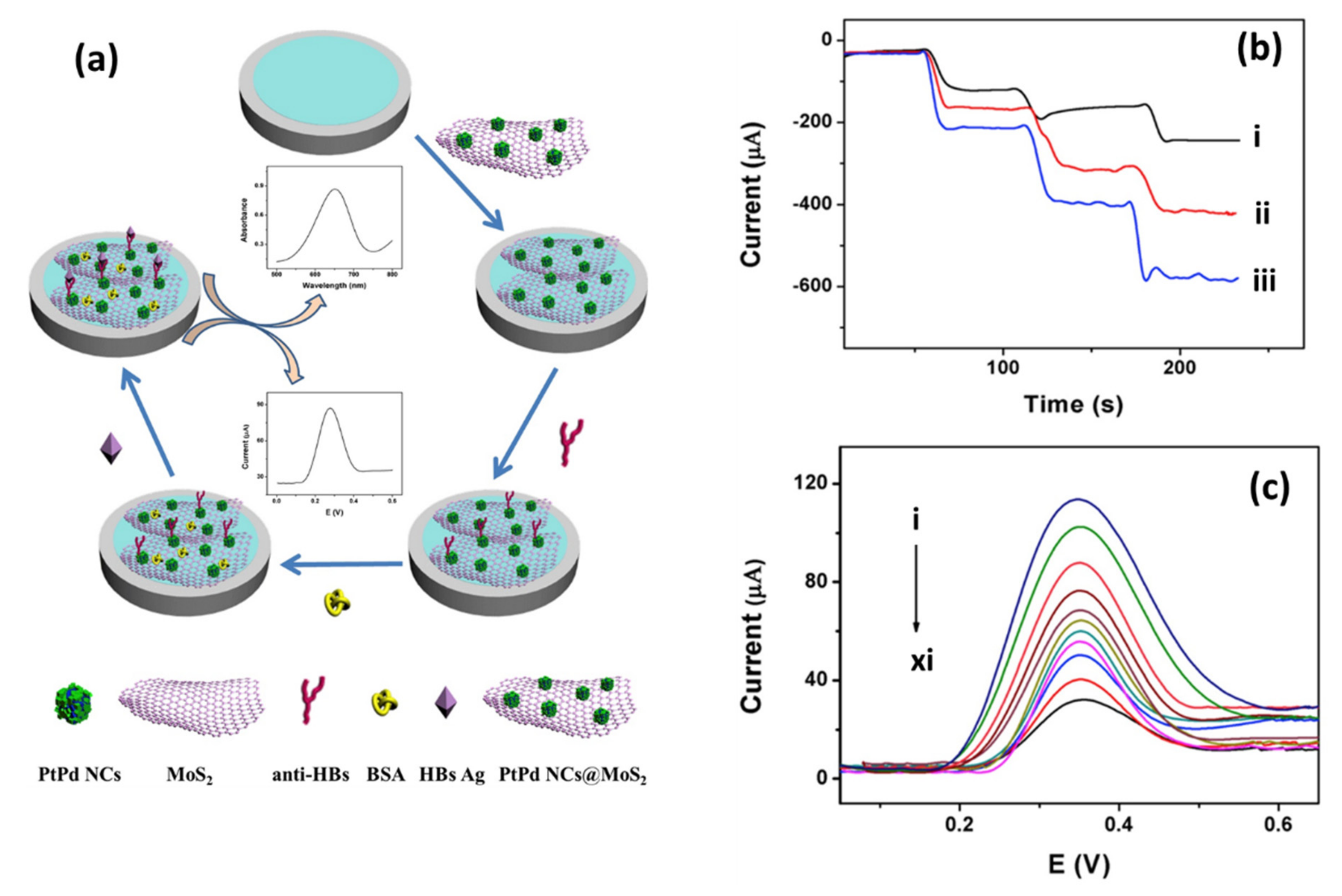
  96. Tan, Z.; Dong, H.; Liu, Q.; Liu, H.; Zhao, P.; Wang, P.; Li, Y.; Zhang, D.; Zhao, Z.; Dong, Y. A Label-Free Immunosensor Based on PtPd NCs@MoS2 Nanoenzymes for Hepatitis B Surface Antigen Detection. Biosens. Bioelectron. 2019, 142, 111556. [Google Scholar] [CrossRef]
  97. Chao, J.; Han, X.; Sun, H.; Su, S.; Weng, L.; Wang, L. Platinum Nanoparticles Supported MoS2 Nanosheet for Simultaneous Detection of Dopamine and Uric Acid. Sci. China Chem. 2016, 59, 332–337. [Google Scholar] [CrossRef]
  98. Sookhakian, M.; Basirun, W.J.; Goh, B.T.; Woi, P.M.; Alias, Y. Molybdenum Disulfide Nanosheet Decorated with Silver Nanoparticles for Selective Detection of Dopamine. Colloids Surf. B Biointerfaces 2019, 176, 80–86. [Google Scholar] [CrossRef] [PubMed]
  99. Zhu, Z.; Jin, C.; Miao, X.; Shen, Y. Simultaneous Determination of Dopamine and Uric Acid on a MoS2-CPtNPs Nanocomposite-Modified Electrode. Int. J. Electrochem. Sci. 2020, 15, 3969–3979. [Google Scholar] [CrossRef]
  100. Dou, B.; Yang, J.; Yuan, R.; Xiang, Y. Trimetallic Hybrid Nanoflower-Decorated MoS2 Nanosheet Sensor for Direct in Situ Monitoring of H2O2 Secreted from Live Cancer Cells. Anal. Chem. 2018, 90, 5945–5950. [Google Scholar] [CrossRef]
  101. Song, D.; Li, Q.; Lu, X.; Li, Y.; Li, Y.; Wang, Y.; Gao, F. Ultra-Thin Bimetallic Alloy Nanowires with Porous Architecture/Monolayer MoS2 Nanosheet as a Highly Sensitive Platform for the Electrochemical Assay of Hazardous Omethoate Pollutant. J. Hazard. Mater. 2018, 357, 466–474. [Google Scholar] [CrossRef]
  102. Ma, N.; Zhang, T.; Fan, D.; Kuang, X.; Ali, A.; Wu, D.; Wei, Q. Triple Amplified Ultrasensitive Electrochemical Immunosensor for Alpha Fetoprotein Detection Based on MoS2@Cu2O-Au Nanoparticles. Sens. Actuators B Chem. 2019, 297, 126821. [Google Scholar] [CrossRef]
  103. Jeevanandham, G.; Jerome, R.; Murugan, N.; Preethika, M.; Vediappan, K.; Sundramoorthy, A.K. Nickel Oxide Decorated MoS2 Nanosheet-Based Non-Enzymatic Sensor for the Selective Detection of Glucose. RSC Adv. 2020, 10, 643–654. [Google Scholar] [CrossRef] [Green Version]
  104. Wang, H.; Chen, P.; Wen, F.; Zhu, Y.; Zhang, Y. Flower-like Fe2O3@MoS2 Nanocomposite Decorated Glassy Carbon Electrode for the Determination of Nitrite. Sens. Actuators B Chem. 2015, 220, 749–754. [Google Scholar] [CrossRef]
  105. Zhang, Y.; Chen, P.; Wen, F.; Yuan, B.; Wang, H. Fe3O4 Nanospheres on MoS2 Nanoflake: Electrocatalysis and Detection of Cr(VI) and Nitrite. J. Electroanal. Chem. 2016, 761, 14–20. [Google Scholar] [CrossRef]
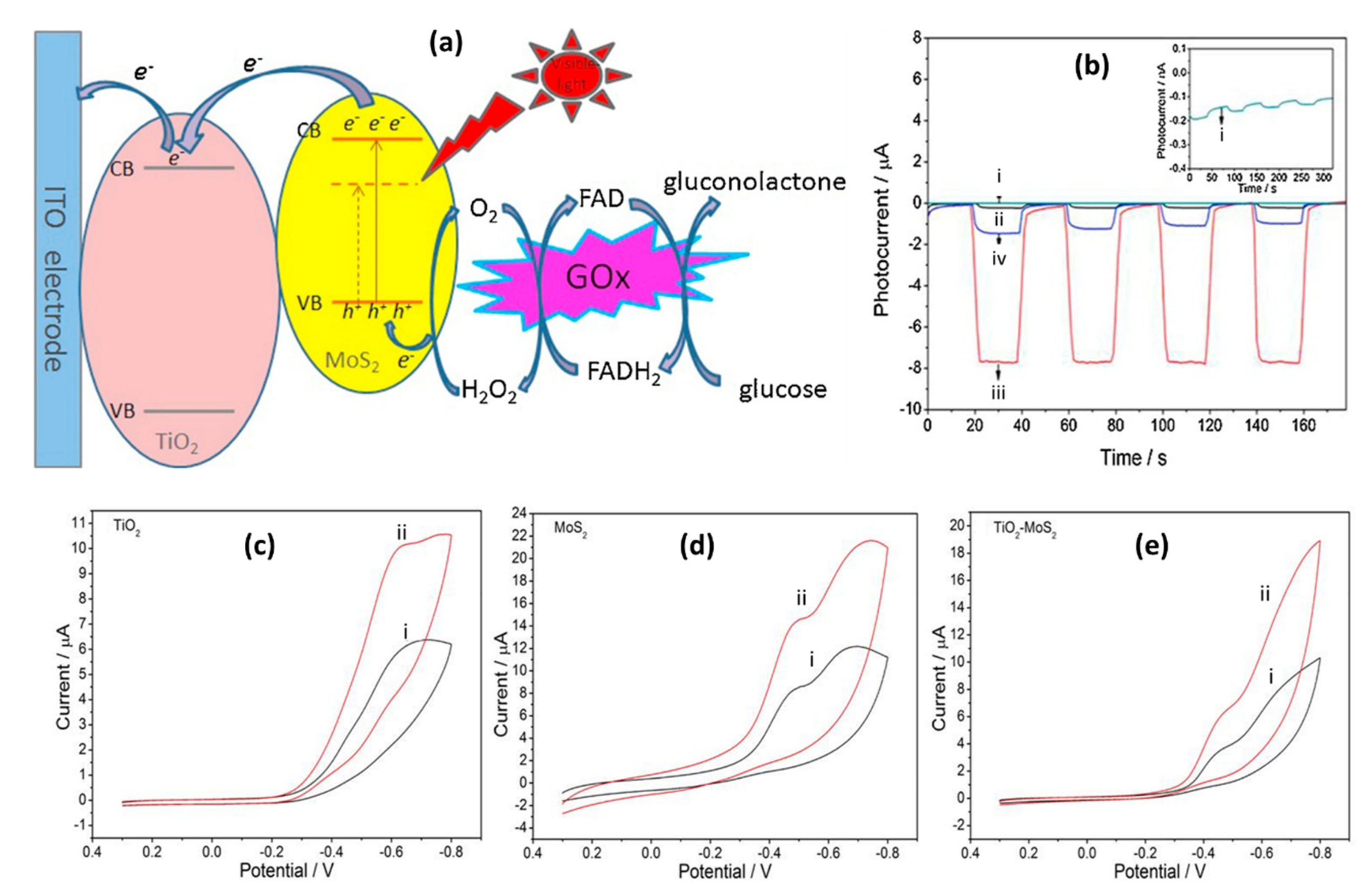
  106. Liu, X.; Huo, X.; Liu, P.; Tang, Y.; Xu, J.; Liu, X.; Zhou, Y. Assembly of MoS2 Nanosheet-TiO2 Nanorod Heterostructure as Sensor Scaffold for Photoelectrochemical Biosensing. Electrochim. Acta 2017, 242, 327–336. [Google Scholar] [CrossRef]
  107. Wang, Y.; Zhao, G.; Zhang, Y.; Pang, X.; Cao, W.; Du, B.; Wei, Q. Sandwich-Type Electrochemical Immunosensor for CEA Detection Based on Ag/MoS2@Fe3O4 and an Analogous ELISA Method with Total Internal Reflection Microscopy. Sens. Actuators B Chem. 2018, 266, 561–569. [Google Scholar] [CrossRef]
  108. Huang, J.; Dong, Z.; Li, Y.; Li, J.; Tang, W.; Yang, H.; Wang, J.; Bao, Y.; Jin, J.; Li, R. MoS2 Nanosheet Functionalized with Cu Nanoparticles and Its Application for Glucose Detection. Mater. Res. Bull. 2013, 48, 4544–4547. [Google Scholar] [CrossRef]
  109. Zhao, H.; Xu, J.; Sheng, Q.; Zheng, J.; Cao, W.; Yue, T. NiCo2O4 Nanorods Decorated MoS2 Nanosheets Synthesized from Deep Eutectic Solvents and Their Application for Electrochemical Sensing of Glucose in Red Wine and Honey. J. Electrochem. Soc. 2019, 166, H404–H411. [Google Scholar] [CrossRef]
  110. Xu, J.; Wang, Y.; Hu, S. Nanocomposites of Graphene and Graphene Oxides: Synthesis, Molecular Functionalization and Application in Electrochemical Sensors and Biosensors. A Review. Microchim. Acta 2017, 184, 1–44. [Google Scholar] [CrossRef]
  111. Bai, S.; Shen, X. Graphene–Inorganic Nanocomposites. RSC Adv. 2012, 2, 64–98. [Google Scholar] [CrossRef]
  112. Liu, M.; Zhu, H.; Wang, Y.; Sevencan, C.; Li, B.L. Functionalized MoS2-Based Nanomaterials for Cancer Phototherapy and Other Biomedical Applications. ACS Mater. Lett. 2021, 3, 462–496. [Google Scholar] [CrossRef]
  113. Souri, Z.; Adeli, M.; Mehdipour, E.; Yari, A.; Shams, A.; Beyranvand, S.; Sattari, S. Covalent Decoration of MoS2 Platforms by Silver Nanoparticles through the Reversible Addition–Fragmentation Chain Transfer Reaction. Langmuir 2021, 37, 3382–3390. [Google Scholar] [CrossRef]
  114. Stergiou, A.; Tagmatarchis, N. Molecular Functionalization of Two-Dimensional MoS2 Nanosheets. Chem. A Eur. J. 2018, 24, 18246–18257. [Google Scholar] [CrossRef]
  115. Zuo, L.-X.; Jiang, L.-P.; Zhu, J.-J. A Facile Sonochemical Route for the Synthesis of MoS2/Pd Composites for Highly Efficient Oxygen Reduction Reaction. Ultrason. Sonochem. 2017, 35, 681–688. [Google Scholar] [CrossRef] [PubMed]
  116. Li, Z.; Wong, S.L. Functionalization of 2D Transition Metal Dichalcogenides for Biomedical Applications. Mater. Sci. Eng. C 2017, 70, 1095–1106. [Google Scholar] [CrossRef] [PubMed]
  117. Mallakpour, S.; Madani, M. A Review of Current Coupling Agents for Modification of Metal Oxide Nanoparticles. Prog. Org. Coat. 2015, 86, 194–207. [Google Scholar] [CrossRef]
  118. Kumar, S.V.; Ganesan, S. Preparation and Characterization of Gold Nanoparticles with Different Capping Agents. Int. J. Green Nanotechnol. 2011, 3, 47–55. [Google Scholar] [CrossRef]
  119. Li, W.; Guo, M.; Zhang, G.; Zhang, Y.W. Edge-Specific Au/Ag Functionalization-Induced Conductive Paths in Armchair MoS2 Nanoribbons. Chem. Mater. 2014, 26, 5625–5631. [Google Scholar] [CrossRef]
  120. Singh, A.; Dahotre, N.B. Laser In-Situ Synthesis of Mixed Carbide Coating on Steel. J. Mater. Sci. 2004, 39, 4553–4560. [Google Scholar] [CrossRef]
  121. Wang, H.Y.; Jiang, Q.C.; Li, X.L.; Wang, J.G. In Situ Synthesis of TiC/Mg Composites in Molten Magnesium. Scr. Mater. 2003, 48, 1349–1354. [Google Scholar] [CrossRef]
  122. Eshun, K.; Xiong, H.D.; Yu, S.; Li, Q. Doping Induces Large Variation in the Electrical Properties of MoS2 Monolayers. Solid. State. Electron. 2015, 106, 44–49. [Google Scholar] [CrossRef]
  123. Viet, N.X.; Hoan, N.X.; Takamura, Y. Development of Highly Sensitive Electrochemical Immunosensor Based on Single-Walled Carbon Nanotube Modified Screen-Printed Carbon Electrode. Mater. Chem. Phys. 2019, 227, 123–129. [Google Scholar] [CrossRef]
  124. Guo, Q.; Ghadiri, R.; Weigel, T.; Aumann, A.; Gurevich, E.L.; Esen, C.; Medenbach, O.; Cheng, W.; Chichkov, B.; Ostendorf, A. Comparison of in Situ and Ex Situ Methods for Synthesis of Two-Photon Polymerization Polymer Nanocomposites. Polymers 2014, 6, 2037–2050. [Google Scholar] [CrossRef]
  125. Adnan, M.M.; Dalod, A.R.M.; Balci, M.H.; Glaum, J.; Einarsrud, M.-A. In Situ Synthesis of Hybrid Inorganic–Polymer Nanocomposites. Polymers 2018, 10, 1129. [Google Scholar] [CrossRef] [Green Version]
  126. Aliofkhazraei, M.; Ali, N. Fabrication and Properties of Micro- and Nanostructured Coatings Using Electrochemical Depositions; Hashmi, S., Batalha, G.F., Van Tyne, C.J., Yilbas, B.B.T.-C.M.P., Eds.; Elsevier: Oxford, UK, 2014; pp. 119–156. [Google Scholar]
  127. Sahoo, P.; Das, S.K.; Davim, J.P. 3.3 Surface Finish Coatings; Hashmi, M.S.J.B.T.-C.M.F., Ed.; Elsevier: Oxford, UK, 2017; pp. 38–55. [Google Scholar]
  128. Karatutlu, A.; Barhoum, A.; Sapelkin, A. Chapter 1—Liquid-Phase Synthesis of Nanoparticles and Nanostructured Materials. In Micro and Nano Technologies; Barhoum, A., Makhlouf, A.S., Barhoum, A., Eds.; Elsevier: Oxford, UK, 2018; pp. 1–28. [Google Scholar]
  129. Bera, D.; Kuiry, S.C.; Seal, S. Synthesis of Nanostructured Materials Using Template-Assisted Electrodeposition. JOM 2004, 56, 49–53. [Google Scholar] [CrossRef]
  130. Cai, Z.; Yao, Q.; Chen, X.; Wang, X. Chapter 14—Nanomaterials With Different Dimensions for Electrocatalysis. In Novel Nanomaterials for Biomedical, Environmental and Energy Applications, Micro and Nano Technologies; Wang, X., Chen, X., Eds.; Elsevier: London, UK, 2019; pp. 435–464. [Google Scholar]
  131. Escoubas, L.; Simon, J.J.; Le Rouzo, J.; Bermudez, V. Innovative Approaches in Thin Film Photovoltaic Cells. In Woodhead Publishing Series in Electronic and Optical Materials; Piegari, A., Flory, F., Eds.; Woodhead Publishing: Cambridge, UK, 2013; pp. 596–630. [Google Scholar]
  132. Yang, S.; Lu, Z.; Luo, S.; Liu, C.; Tang, Y. Direct Electrodeposition of a Biocomposite Consisting of Reduced Graphene Oxide, Chitosan and Glucose Oxidase on a Glassy Carbon Electrode for Direct Sensing of Glucose. Microchim. Acta 2013, 180, 127–135. [Google Scholar] [CrossRef]
  133. Feng, S.-H.; Li, G.-H. Chapter 4—Hydrothermal and Solvothermal Syntheses. In Modern Inorganic Synthetic Chemistry, 2nd ed.; Xu, R., Xu, Y., Eds.; Elsevier: Amsterdam, The Netherlands, 2017; pp. 73–104. [Google Scholar]
  134. Byrappa, K.; Yoshimura, M. Hydrothermal Technology—Principles and Applications. In Handbook of Hydrothermal Technology; Byrappa, K., Yoshimura, M.B.T.-H., Eds.; William Andrew Publishing: Norwich, NY, USA, 2001; pp. 1–52. [Google Scholar]
  135. Dang, T.M.D.; Le, T.T.T.; Fribourg-Blanc, E.; Dang, M.C. Synthesis and Optical Properties of Copper Nanoparticles Prepared by a Chemical Reduction Method. Adv. Nat. Sci. Nanosci. Nanotechnol. 2011, 2, 15009. [Google Scholar] [CrossRef]
  136. Lee, S.M.; Song, K.C.; Lee, B.S. Antibacterial Activity of Silver Nanoparticles Prepared by a Chemical Reduction Method. Korean J. Chem. Eng. 2010, 27, 688–692. [Google Scholar] [CrossRef]
  137. Govindasamy, M.; Mani, V.; Chen, S.M.; Karthik, R.; Manibalan, K.; Umamaheswari, R. MoS2 Flowers Grown on Graphene/Carbon Nanotubes: A Versatile Substrate for Electrochemical Determination of Hydrogen Peroxide. Int. J. Electrochem. Sci. 2016, 11, 2954–2961. [Google Scholar] [CrossRef]
  138. Li, C.; Zhang, D.; Wang, J.; Hu, P.; Jiang, Z. Magnetic MoS2 on Multiwalled Carbon Nanotubes for Sulfide Sensing. Anal. Chim. Acta 2017, 975, 61–69. [Google Scholar] [CrossRef]
  139. Yang, T.; Chen, H.; Ge, T.; Wang, J.; Li, W.; Jiao, K. Highly Sensitive Determination of Chloramphenicol Based on Thin-Layered MoS2/Polyaniline Nanocomposite. Talanta 2015, 144, 1324–1328. [Google Scholar] [CrossRef]
  140. Sadeghi, M.; Jahanshahi, M.; Javadian, H. Highly Sensitive Biosensor for Detection of DNA Nucleobases: Enhanced Electrochemical Sensing Based on Polyaniline/Single-Layer MoS2 Nanosheets Nanocomposite Modified Carbon Paste Electrode. Microchem. J. 2020, 152, 104315. [Google Scholar] [CrossRef]
  141. Li, Y.; Lin, H.; Peng, H.; Qi, R.; Luo, C. A Glassy Carbon Electrode Modified with MoS2 Nanosheets and Poly(3,4-Ethylenedioxythiophene) for Simultaneous Electrochemical Detection of Ascorbic Acid, Dopamine and Uric Acid. Microchim. Acta 2016, 183, 2517–2523. [Google Scholar] [CrossRef]
  142. Huang, K.-J.; Wang, L.; Li, J.; Liu, Y.-M. Electrochemical Sensing Based on Layered MoS2–Graphene Composites. Sens. Actuators B Chem. 2013, 178, 671–677. [Google Scholar] [CrossRef]
  143. Lee, C.; Rathi, S.; Khan, M.A.; Lim, D.; Kim, Y.; Yun, S.J.; Youn, D.-H.; Watanabe, K.; Taniguchi, T.; Kim, G.-H. Comparison of Trapped Charges and Hysteresis Behavior in HBN Encapsulated Single MoS2 Flake Based Field Effect Transistors on SiO2 and HBN Substrates. Nanotechnology 2018, 29, 335202. [Google Scholar] [CrossRef]
  144. Mak, K.F.; Lee, C.; Hone, J.; Shan, J.; Heinz, T.F. Atomically thin MoS 2: A new direct-gap semiconductor. Phys. Rev. Lett. 2010, 105, 136805. [Google Scholar] [CrossRef] [PubMed] [Green Version]
  145. Kadantsev, E.S.; Hawrylak, P. Electronic Structure of a Single MoS2 Monolayer. Solid State Commun. 2012, 152, 909–913. [Google Scholar] [CrossRef]
  146. Kuc, A.; Zibouche, N.; Heine, T. Influence of Quantum Confinement on the Electronic Structure of the Transition Metal Sulfide T S 2. Phys. Rev. B 2011, 83, 245213. [Google Scholar] [CrossRef] [Green Version]
  147. Li, T.; Galli, G. Electronic Properties of MoS2 Nanoparticles. J. Phys. Chem. C 2007, 111, 16192–16196. [Google Scholar] [CrossRef]
  148. Splendiani, A.; Sun, L.; Zhang, Y.; Li, T.; Kim, J.; Chim, C.-Y.; Galli, G.; Wang, F. Emerging Photoluminescence in Monolayer MoS2. Nano Lett. 2010, 10, 1271–1275. [Google Scholar] [CrossRef] [PubMed]
  149. Chhowalla, M.; Shin, H.S.; Eda, G.; Li, L.-J.; Loh, K.P.; Zhang, H. The Chemistry of Two-Dimensional Layered Transition Metal Dichalcogenide Nanosheets. Nat. Chem. 2013, 5, 263–275. [Google Scholar] [CrossRef]
  150. Kim, I.S.; Sangwan, V.K.; Jariwala, D.; Wood, J.D.; Park, S.; Chen, K.-S.; Shi, F.; Ruiz-Zepeda, F.; Ponce, A.; Jose-Yacaman, M.; et al. Influence of Stoichiometry on the Optical and Electrical Properties of Chemical Vapor Deposition Derived MoS2. ACS Nano 2014, 8, 10551–10558. [Google Scholar] [CrossRef] [Green Version]
  151. Chaabani, R.; Lamouchi, A.; Mari, B.; Chtourou, R. Effect of Sulfurization on Physical and Electrical Properties of MoS2 Films Synthesized by Electrodeposition Route. Mater. Res. Express 2019, 6, 115902. [Google Scholar] [CrossRef]
  152. Zhan, Y.; Liu, Z.; Najmaei, S.; Ajayan, P.M.; Lou, J. Large-Area Vapor-Phase Growth and Characterization of MoS2 Atomic Layers on a SiO2 Substrate. Small 2012, 8, 966–971. [Google Scholar] [CrossRef] [PubMed] [Green Version]
  153. Chamlagain, B.; Bhanu, U.; Mou, S.; Khondaker, S.I. Tailoring the Potential Landscape and Electrical Properties of 2D MoS2 Using Gold Nanostructures of Different Coverage Density. J. Phys. Chem. C 2020, 124, 6461–6466. [Google Scholar] [CrossRef]
  154. Wang, S.Y.; Ko, T.S.; Huang, C.C.; Lin, D.Y.; Huang, Y.S. Optical and Electrical Properties of MoS2and Fe-Doped MoS2. Jpn. J. Appl. Phys. 2014, 53, 04EH07. [Google Scholar] [CrossRef]
  155. Da Cunha, W.F.; dos Santos, R.M.; de Sousa Júnior, R.T.; Santos, R.B.; e Silva, G.M.; Ribeiro Júnior, L.A. Tuning the Electronic Structure Properties of MoS2 Monolayers with Carbon Doping. Phys. Chem. Chem. Phys. 2019, 21, 11168–11174. [Google Scholar] [CrossRef]
  156. Zhao, X.; Chen, P.; Xia, C.; Wang, T.; Dai, X. Electronic and Magnetic Properties of N-Type and p-Doped MoS2 Monolayers. RSC Adv. 2016, 6, 16772–16778. [Google Scholar] [CrossRef]
  157. Khan, M.F.; Nazir, G.; Lermolenko, V.M.; Eom, J. Electrical and Photo-Electrical Properties of MoS2 Nanosheets with and without an Al2O3 Capping Layer under Various Environmental Conditions. Sci. Technol. Adv. Mater. 2016, 17, 166–176. [Google Scholar] [CrossRef] [Green Version]
  158. Bonaccorso, F.; Bartolotta, A.; Coleman, J.N.; Backes, C. 2D-Crystal-Based Functional Inks. Adv. Mater. 2016, 28, 6136–6166. [Google Scholar] [CrossRef]
  159. El-Mahalawy, S.H.; Evans, B.L. Temperature Dependence of the Electrical Conductivity and Hall Coefficient in 2H-MoS2, MoSe2, WSe2, and MoTe2. Phys. Status Solidi 1977, 79, 713–722. [Google Scholar] [CrossRef]
  160. El-Mahalawy, S.H.; Evans, B.L. Pressure Dependence of the Electrical Conductivity in 2H-MoS2 and 2H-WSe2. Phys. Status Solidi 1978, 86, 151–157. [Google Scholar] [CrossRef]
  161. Kim, E.; Lee, Y.; Ko, C.; Park, Y.; Yeo, J.; Chen, Y.; Choe, H.S.; Allen, F.I.; Rho, J.; Tongay, S.; et al. Tuning the Optical and Electrical Properties of MoS2 by Selective Ag Photo-Reduction. Appl. Phys. Lett. 2018, 113, 13105. [Google Scholar] [CrossRef]
  162. Wilcoxon, J.P.; Newcomer, P.P.; Samara, G.A. Synthesis and Optical Properties of MoS2 and Isomorphous Nanoclusters in the Quantum Confinement Regime. J. Appl. Phys. 1997, 81, 7934–7944. [Google Scholar] [CrossRef]
  163. Edvinsson, T. Optical Quantum Confinement and Photocatalytic Properties in Two-, One- and Zero-Dimensional Nanostructures. R. Soc. Open Sci. 2020, 5, 180387. [Google Scholar] [CrossRef] [Green Version]
  164. Qiao, W.; Yan, S.; Song, X.; Zhang, X.; He, X.; Zhong, W.; Du, Y. Luminescent Monolayer MoS2 Quantum Dots Produced by Multi-Exfoliation Based on Lithium Intercalation. Appl. Surf. Sci. 2015, 359, 130–136. [Google Scholar] [CrossRef]
  165. Molina-Sánchez, A.; Hummer, K.; Wirtz, L. Vibrational and Optical Properties of MoS2: From Monolayer to Bulk. Surf. Sci. Rep. 2015, 70, 554–586. [Google Scholar] [CrossRef] [Green Version]
  166. Yim, C.; O’Brien, M.; McEvoy, N.; Winters, S.; Mirza, I.; Lunney, J.G.; Duesberg, G.S. Investigation of the Optical Properties of MoS2 Thin Films Using Spectroscopic Ellipsometry. Appl. Phys. Lett. 2014, 104, 103114. [Google Scholar] [CrossRef] [Green Version]
  167. Sundaram, R.S.; Engel, M.; Lombardo, A.; Krupke, R.; Ferrari, A.C.; Avouris, P.; Steiner, M. Electroluminescence in Single Layer MoS2. Nano Lett. 2013, 13, 1416–1421. [Google Scholar] [CrossRef] [Green Version]
  168. Vikraman, D.; Akbar, K.; Hussain, S.; Yoo, G.; Jang, J.-Y.; Chun, S.-H.; Jung, J.; Park, H.J. Direct Synthesis of Thickness-Tunable MoS2 Quantum Dot Thin Layers: Optical, Structural and Electrical Properties and Their Application to Hydrogen Evolution. Nano Energy 2017, 35, 101–114. [Google Scholar] [CrossRef]
  169. Li, W.; Birdwell, A.G.; Amani, M.; Burke, R.A.; Ling, X.; Lee, Y.-H.; Liang, X.; Peng, L.; Richter, C.A.; Kong, J.; et al. Broadband Optical Properties of Large-Area Monolayer CVD Molybdenum Disulfide. Phys. Rev. B 2014, 90, 195434. [Google Scholar] [CrossRef] [Green Version]
  170. Lee, C.; Yan, H.; Brus, L.E.; Heinz, T.F.; Hone, J.; Ryu, S. Anomalous Lattice Vibrations of Single- and Few-Layer MoS2. ACS Nano 2010, 4, 2695–2700. [Google Scholar] [CrossRef] [Green Version]
  171. Ye, M.; Winslow, D.; Zhang, D.; Pandey, R.; Yap, Y.K. Recent Advancement on the Optical Properties of Two-Dimensional Molybdenum Disulfide (MoS2) Thin Films. Photonics 2015, 2, 288–307. [Google Scholar] [CrossRef] [Green Version]
  172. Wang, G.; Xu, J.; Chen, H. Progress in the Studies of Photoelectrochemical Sensors. Sci. China Ser. B Chem. 2009, 52, 1789. [Google Scholar] [CrossRef]
  173. Shu, J.; Tang, D. Recent Advances in Photoelectrochemical Sensing: From Engineered Photoactive Materials to Sensing Devices and Detection Modes. Anal. Chem. 2020, 92, 363–377. [Google Scholar] [CrossRef] [PubMed]
  174. Zang, Y.; Lei, J.; Ju, H. Principles and Applications of Photoelectrochemical Sensing Strategies Based on Biofunctionalized Nanostructures. Biosens. Bioelectron. 2017, 96, 8–16. [Google Scholar] [CrossRef]
  175. Qiu, Z.; Tang, D. Nanostructure-Based Photoelectrochemical Sensing Platforms for Biomedical Applications. J. Mater. Chem. B 2020, 8, 2541–2561. [Google Scholar] [CrossRef] [PubMed]
  176. Hun, X.; Wang, S.; Wang, S.; Zhao, J.; Luo, X. A Photoelectrochemical Sensor for Ultrasensitive Dopamine Detection Based on Single-Layer NanoMoS2 Modified Gold Electrode. Sens. Actuators B Chem. 2017, 249, 83–89. [Google Scholar] [CrossRef]
  177. Wang, X.; Deng, H.; Wang, C.; Wei, Q.; Wang, Y.; Xiong, X.; Li, C.; Li, W. A Pro-Gastrin-Releasing Peptide Imprinted Photoelectrochemical Sensor Based on the in Situ Growth of Gold Nanoparticles on a MoS2 Nanosheet Surface. Analyst 2020, 145, 1302–1309. [Google Scholar] [CrossRef]
  178. Shi, Y.; Zhang, Q.; Zhai, T.-T.; Zhou, Y.; Yang, D.-R.; Wang, F.-B.; Xia, X.-H. Localized Surface Plasmon Resonance Enhanced Label-Free Photoelectrochemical Immunoassay by Au-MoS2 Nanohybrid. Electrochim. Acta 2018, 271, 361–369. [Google Scholar] [CrossRef]
  179. Zhou, W.; Yin, Z.; Du, Y.; Huang, X.; Zeng, Z.; Fan, Z.; Liu, H.; Wang, J.; Zhang, H. Synthesis of Few-Layer MoS2 Nanosheet-Coated TiO2 Nanobelt Heterostructures for Enhanced Photocatalytic Activities. Small 2013, 9, 140–147. [Google Scholar] [CrossRef]
  180. Ma, C.; Cao, Y.; Gou, X.; Zhu, J.-J. Recent Progress in Electrochemiluminescence Sensing and Imaging. Anal. Chem. 2020, 92, 431–454. [Google Scholar] [CrossRef]
  181. Li, L.; Chen, Y.; Zhu, J.-J. Recent Advances in Electrochemiluminescence Analysis. Anal. Chem. 2017, 89, 358–371. [Google Scholar] [CrossRef]
  182. Truong, C.K.P.; Nguyen, T.D.D.; Shin, I.-S. Electrochemiluminescent Chemosensors for Clinical Applications: A Review. BioChip J. 2019, 13, 203–216. [Google Scholar] [CrossRef]
  183. Rizwan, M.; Mohd-Naim, N.F.; Ahmed, M.U. Trends and Advances in Electrochemiluminescence Nanobiosensors. Sensors 2018, 18, 166. [Google Scholar] [CrossRef] [Green Version]
  184. Miao, W. 13—Electrogenerated Chemiluminescence. In Handbook of Electrochemistry; Zoski, C.G., Ed.; Elsevier: Amsterdam, The Netherlands, 2007; pp. 541–590. [Google Scholar]
  185. Chen, Y.; Cao, Y.; Ma, C.; Zhu, J.-J. Carbon-Based Dots for Electrochemiluminescence Sensing. Mater. Chem. Front. 2020, 4, 369–385. [Google Scholar] [CrossRef]
  186. Li, Y.; Wang, Y.; Bai, L.; Lv, H.; Huang, W.; Liu, S.; Ding, S.; Zhao, M. Ultrasensitive Electrochemiluminescent Immunosensing Based on Trimetallic Au–Pd–Pt/MoS2 Nanosheet as Coreaction Accelerator and Self-Enhanced ABEI-Centric Complex. Anal. Chim. Acta 2020, 1125, 86–93. [Google Scholar] [CrossRef]
  187. Liu, Y.-M.; Zhou, M.; Liu, Y.-Y.; Shi, G.-F.; Zhang, J.-J.; Cao, J.-T.; Huang, K.-J.; Chen, Y.-H. Fabrication of Electrochemiluminescence Aptasensor Based on in Situ Growth of Gold Nanoparticles on Layered Molybdenum Disulfide for Sensitive Detection of Platelet-Derived Growth Factor-BB. RSC Adv. 2014, 4, 22888–22893. [Google Scholar] [CrossRef]
  188. Kalantar-zadeh, K.; Ou, J.Z. Biosensors Based on Two-Dimensional MoS2. ACS Sensors 2016, 1, 5–16. [Google Scholar] [CrossRef]
  189. Karunadasa, H.I.; Montalvo, E.; Sun, Y.; Majda, M.; Long, J.R.; Chang, C.J. A Molecular MoS2 Edge Site Mimic for Catalytic Hydrogen Generation. Science 2012, 335, 698–702. [Google Scholar] [CrossRef] [Green Version]
  190. Tuxen, A.; Kibsgaard, J.; Gøbel, H.; Lægsgaard, E.; Topsøe, H.; Lauritsen, J.V.; Besenbacher, F. Size Threshold in the Dibenzothiophene Adsorption on MoS2 Nanoclusters. ACS Nano 2010, 4, 4677–4682. [Google Scholar] [CrossRef]
  191. Chia, X.; Ambrosi, A.; Sedmidubský, D.; Sofer, Z.; Pumera, M. Precise Tuning of the Charge Transfer Kinetics and Catalytic Properties of MoS2 Materials via Electrochemical Methods. Chem. A Eur. J. 2014, 20, 17426–17432. [Google Scholar] [CrossRef]
  192. Wang, D.; Wang, Z.; Wang, C.; Zhou, P.; Wu, Z.; Liu, Z. Distorted MoS2 Nanostructures: An Efficient Catalyst for the Electrochemical Hydrogen Evolution Reaction. Electrochem. Commun. 2013, 34, 219–222. [Google Scholar] [CrossRef]
  193. Ambrosi, A.; Chia, X.; Sofer, Z.; Pumera, M. Enhancement of Electrochemical and Catalytic Properties of MoS2 through Ball-Milling. Electrochem. Commun. 2015, 54, 36–40. [Google Scholar] [CrossRef]
  194. Lauritsen, J.V.; Kibsgaard, J.; Olesen, G.H.; Moses, P.G.; Hinnemann, B.; Helveg, S.; Nørskov, J.K.; Clausen, B.S.; Topsøe, H.; Lægsgaard, E.; et al. Location and Coordination of Promoter Atoms in Co- and Ni-Promoted MoS2-Based Hydrotreating Catalysts. J. Catal. 2007, 249, 220–233. [Google Scholar] [CrossRef]
  195. Keçili, R.; Büyüktiryaki, S.; Hussain, C.M. Chapter 57—Engineered Nanosensors Based on Molecular Imprinting Technology. In Micro and Nano Technologies; Hussain, C.M., Ed.; Elsevier: Amsterdam, The Netherlands, 2018; pp. 1031–1046. [Google Scholar]
  196. Ananda Murthy, H.C.; Wagassa, A.N.; Ravikumar, C.R.; Nagaswarupa, H.P. 17—Functionalized Metal and Metal Oxide Nanomaterial-Based Electrochemical Sensors. In Woodhead Publishing Series in Electronic and Optical Materials; Hussain, C.M., Manjunatha, J.G., Eds.; Woodhead Publishing: Cambridge, UK, 2022; pp. 369–392. [Google Scholar]
  197. Yogeswaran, U.; Chen, S.-M. A Review on the Electrochemical Sensors and Biosensors Composed of Nanowires as Sensing Material. Sensors 2008, 8, 290–313. [Google Scholar] [CrossRef] [PubMed] [Green Version]
  198. Chao, J.; Zou, M.; Zhang, C.; Sun, H.; Pan, D.; Pei, H.; Su, S.; Yuwen, L.; Fan, C.; Wang, L. A MoS2–Based System for Efficient Immobilization of Hemoglobin and Biosensing Applications. Nanotechnology 2015, 26, 274005. [Google Scholar] [CrossRef]
  199. Yang, H. Enzyme-Based Ultrasensitive Electrochemical Biosensors. Curr. Opin. Chem. Biol. 2012, 16, 422–428. [Google Scholar] [CrossRef]
  200. Putzbach, W.; Ronkainen, N.J. Immobilization Techniques in the Fabrication of Nanomaterial-Based Electrochemical Biosensors: A Review. Sensors 2013, 13, 4811–4840. [Google Scholar] [CrossRef]
  201. Wang, X.; Nan, F.; Zhao, J.; Yang, T.; Ge, T.; Jiao, K. A Label-Free Ultrasensitive Electrochemical DNA Sensor Based on Thin-Layer MoS2 Nanosheets with High Electrochemical Activity. Biosens. Bioelectron. 2015, 64, 386–391. [Google Scholar] [CrossRef]
  202. Sha, R.; Vishnu, N.; Badhulika, S. MoS2 Based Ultra-Low-Cost, Flexible, Non-Enzymatic and Non-Invasive Electrochemical Sensor for Highly Selective Detection of Uric Acid in Human Urine Samples. Sens. Actuators B Chem. 2019, 279, 53–60. [Google Scholar] [CrossRef]
  203. Tan, C.; Zhang, H. Two-Dimensional Transition Metal Dichalcogenide Nanosheet-Based Composites. Chem. Soc. Rev. 2015, 44, 2713–2731. [Google Scholar] [CrossRef]
  204. Bankar, S.B.; Bule, M.V.; Singhal, R.S.; Ananthanarayan, L. Glucose Oxidase—An Overview. Biotechnol. Adv. 2009, 27, 489–501. [Google Scholar] [CrossRef]
  205. Zhai, Y.; Zhai, S.; Chen, G.; Zhang, K.; Yue, Q.; Wang, L.; Liu, J.; Jia, J. Effects of Morphology of Nanostructured ZnO on Direct Electrochemistry and Biosensing Properties of Glucose Oxidase. J. Electroanal. Chem. 2011, 656, 198–205. [Google Scholar] [CrossRef]
  206. Ma, K.; Sinha, A.; Dang, X.; Zhao, H. Electrochemical Preparation of Gold Nanoparticles-Polypyrrole Co-Decorated 2D MoS2 Nanocomposite Sensor for Sensitive Detection of Glucose. J. Electrochem. Soc. 2019, 166, B147–B154. [Google Scholar] [CrossRef]
  207. Waqas, M.; Zulfiqar, A.; Ahmad, H.B.; Akhtar, N.; Hussain, M.; Shafiq, Z.; Abbas, Y.; Mehmood, K.; Ajmal, M.; Yang, M. Fabrication of Highly Stable Silver Nanoparticles with Shape-Dependent Electrochemical Efficacy. Electrochim. Acta 2018, 271, 641–651. [Google Scholar] [CrossRef]
  208. Su, S.; Cao, W.; Liu, W.; Lu, Z.; Zhu, D.; Chao, J.; Weng, L.; Wang, L.; Fan, C.; Wang, L. Dual-Mode Electrochemical Analysis of MicroRNA-21 Using Gold Nanoparticle-Decorated MoS2 Nanosheet. Biosens. Bioelectron. 2017, 94, 552–559. [Google Scholar] [CrossRef]
  209. Lin, X.; Ni, Y.; Kokot, S. Electrochemical Cholesterol Sensor Based on Cholesterol Oxidase and MoS2-AuNPs Modified Glassy Carbon Electrode. Sens. Actuators B Chem. 2016, 233, 100–106. [Google Scholar] [CrossRef]
  210. Yang, Y.; Zhang, H.; Huang, C.; Yang, D.; Jia, N. Electrochemical Non-Enzyme Sensor for Detecting Clenbuterol (CLB) Based on MoS2-Au-PEI-Hemin Layered Nanocomposites. Biosens. Bioelectron. 2017, 89, 461–467. [Google Scholar] [CrossRef]
  211. Bao, J.; Qi, Y.; Huo, D.; Hou, J.; Geng, X.; Samalo, M.; Liu, Z.; Luo, H.; Yang, M.; Hou, C. A Sensitive and Selective Non-Enzymatic Glucose Sensor Based on AuNPs/CuO NWs-MoS2 Modified Electrode. J. Electrochem. Soc. 2019, 166, B1179–B1185. [Google Scholar] [CrossRef]
  212. Lin, M.; Wan, H.; Zhang, J.; Wang, Q.; Hu, X.; Xia, F. Electrochemical DNA Sensors Based on MoS2-AuNPs for Polynucleotide Kinase Activity and Inhibition Assay. ACS Appl. Mater. Interfaces 2020, 12, 45814–45821. [Google Scholar] [CrossRef]
  213. Liu, L.; Zhu, S.; Wei, Y.; Liu, X.; Jiao, S.; Yang, J. Ultrasensitive Detection of MiRNA-155 Based on Controlled Fabrication of AuNPs@MoS2 Nanostructures by Atomic Layer Deposition. Biosens. Bioelectron. 2019, 144, 111660. [Google Scholar] [CrossRef]
  214. Zhang, B.; Zhang, Y.; Liang, W.; Yu, X.; Tan, H.; Wang, G.; Li, A.; Jin, J.; Huang, L. Copper Sulfide-Functionalized Molybdenum Disulfide Nanohybrids as Nanoenzyme Mimics for Electrochemical Immunoassay of Myoglobin in Cardiovascular Disease. RSC Adv. 2017, 7, 2486–2493. [Google Scholar] [CrossRef] [Green Version]
  215. Wan, Y.; Su, Y.; Zhu, X.; Liu, G.; Fan, C. Development of Electrochemical Immunosensors towards Point of Care Diagnostics. Biosens. Bioelectron. 2013, 47, 1–11. [Google Scholar] [CrossRef] [PubMed]
  216. Liu, G.; Lin, Y. Nanomaterial Labels in Electrochemical Immunosensors and Immunoassays. Talanta 2007, 74, 308–317. [Google Scholar] [CrossRef] [PubMed] [Green Version]
  217. Kukkar, M.; Tuteja, S.K.; Kumar, P.; Kim, K.-H.; Bhadwal, A.S.; Deep, A. A Novel Approach for Amine Derivatization of MoS2 Nanosheets and Their Application toward Label-Free Immunosensor. Anal. Biochem. 2018, 555, 1–8. [Google Scholar] [CrossRef] [PubMed]
  218. Bohli, N.; Belkilani, M.; Mora, L.; Abdelghani, A. Antibody-Functionalised Gold Nanoparticles-Based Impedimetric Immunosensor: Detection Methods for Better Sensitivity. Micro Nano Lett. 2019, 14, 629–633. [Google Scholar] [CrossRef]
  219. Li, Q.; Liu, D.; Xu, L.; Xing, R.; Liu, W.; Sheng, K.; Song, H. Wire-in-Tube IrOx Architectures: Alternative Label-Free Immunosensor for Amperometric Immunoassay toward α-Fetoprotein. ACS Appl. Mater. Interfaces 2015, 7, 22719–22726. [Google Scholar] [CrossRef]
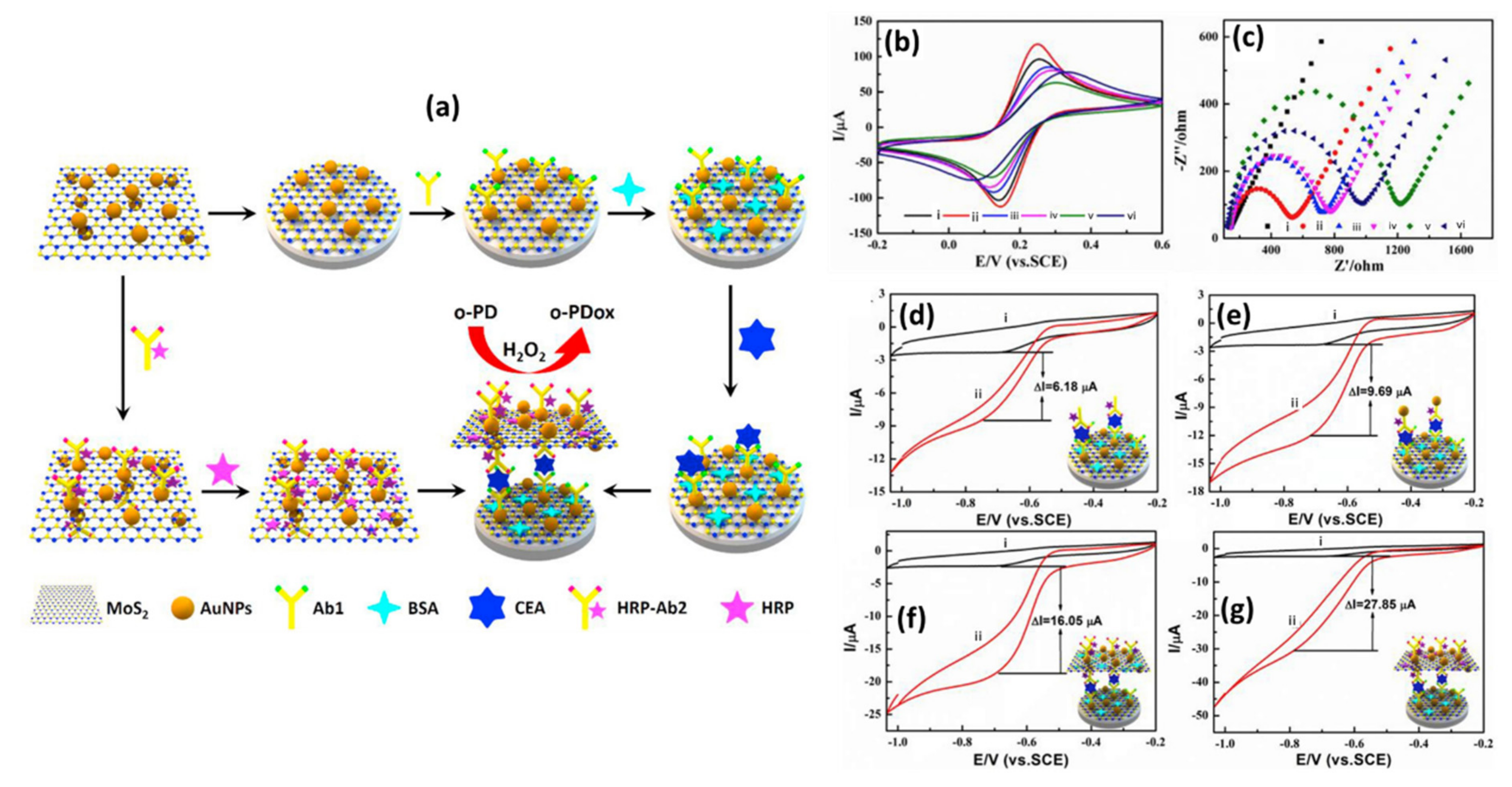
  220. Su, S.; Sun, Q.; Wan, L.; Gu, X.; Zhu, D.; Zhou, Y.; Chao, J.; Wang, L. Ultrasensitive Analysis of Carcinoembryonic Antigen Based on MoS2-Based Electrochemical Immunosensor with Triple Signal Amplification. Biosens. Bioelectron. 2019, 140, 111353. [Google Scholar] [CrossRef]
  221. Wang, X.; Chu, C.; Shen, L.; Deng, W.; Yan, M.; Ge, S.; Yu, J.; Song, X. An Ultrasensitive Electrochemical Immunosensor Based on the Catalytical Activity of MoS2-Au Composite Using Ag Nanospheres as Labels. Sens. Actuators B Chem. 2015, 206, 30–36. [Google Scholar] [CrossRef]
  222. Ding, H.; Yang, L.; Jia, H.; Fan, D.; Zhang, Y.; Sun, X.; Wei, Q.; Ju, H. Label-Free Electrochemical Immunosensor with Palladium Nanoparticles Functionalized MoS2/NiCo Heterostructures for Sensitive Procalcitonin Detection. Sens. Actuators B Chem. 2020, 312, 127980. [Google Scholar] [CrossRef]
  223. Yagati, A.K.; Go, A.; Vu, N.H.; Lee, M.-H. A MoS2–Au Nanoparticle-Modified Immunosensor for T3 Biomarker Detection in Clinical Serum Samples. Electrochim. Acta 2020, 342, 136065. [Google Scholar] [CrossRef]
  224. Giang, H.; Pali, M.; Fan, L.; Suni, I.I. Impedance Biosensing atop MoS2 Thin Films with Mo−S Bond Formation to Antibody Fragments Created by Disulphide Bond Reduction. Electroanalysis 2019, 31, 957–965. [Google Scholar] [CrossRef]
  225. Zhang, Z.; Zhang, Y.; Yu, H.; Rong, S.; Gao, H.; Meng, L.; Dai, J.; Pan, H.; Chang, D. Spherical Carrier Amplification Strategy for Electrochemical Immunosensor Based on Polystyrene-Gold Nanorods @L-Cysteine/MoS2 for Determination of Tacrolimus. Talanta 2020, 220, 121321. [Google Scholar] [CrossRef]
  226. Zhou, Q.; Tang, D. Recent Advances in Photoelectrochemical Biosensors for Analysis of Mycotoxins in Food. TrAC Trends Anal. Chem. 2020, 124, 115814. [Google Scholar] [CrossRef]
  227. Syrek, K.; Skolarczyk, M.; Zych, M.; Sołtys-Mróz, M.; Sulka, G.D. A Photoelectrochemical Sensor Based on Anodic TiO2 for Glucose Determination. Sensors 2019, 19, 4981. [Google Scholar] [CrossRef] [Green Version]
  228. Liu, W.; Zhan, W.; Jia, X.; Liu, Q.; Chen, R.; Li, D.; Huang, Y.; Zhang, G.; Ni, H. Rapid Synthesis of Vertically-Aligned Zinc Oxide Nanorods on Stainless Steel for Non-Enzymatic Glucose and H2O2 Photoelectrochemical Sensor. Appl. Surf. Sci. 2019, 480, 341–348. [Google Scholar] [CrossRef]
  229. Zhang, N.; Ruan, Y.-F.; Ma, Z.-Y.; Zhao, W.-W.; Xu, J.-J.; Chen, H.-Y. Simultaneous Photoelectrochemical and Visualized Immunoassay of β-Human Chorionic Gonadotrophin. Biosens. Bioelectron. 2016, 85, 294–299. [Google Scholar] [CrossRef]
  230. Wang, Y.; Zhou, Y.; Xu, L.; Han, Z.; Yin, H.; Ai, S. Photoelectrochemical Apta-Biosensor for Zeatin Detection Based on Graphene Quantum Dots Improved Photoactivity of Graphite-like Carbon Nitride and Streptavidin Induced Signal Inhibition. Sens. Actuators B Chem. 2018, 257, 237–244. [Google Scholar] [CrossRef]
  231. Wu, P.; Shao, Q.; Hu, Y.; Jin, J.; Yin, Y.; Zhang, H.; Cai, C. Direct Electrochemistry of Glucose Oxidase Assembled on Graphene and Application to Glucose Detection. Electrochim. Acta 2010, 55, 8606–8614. [Google Scholar] [CrossRef]
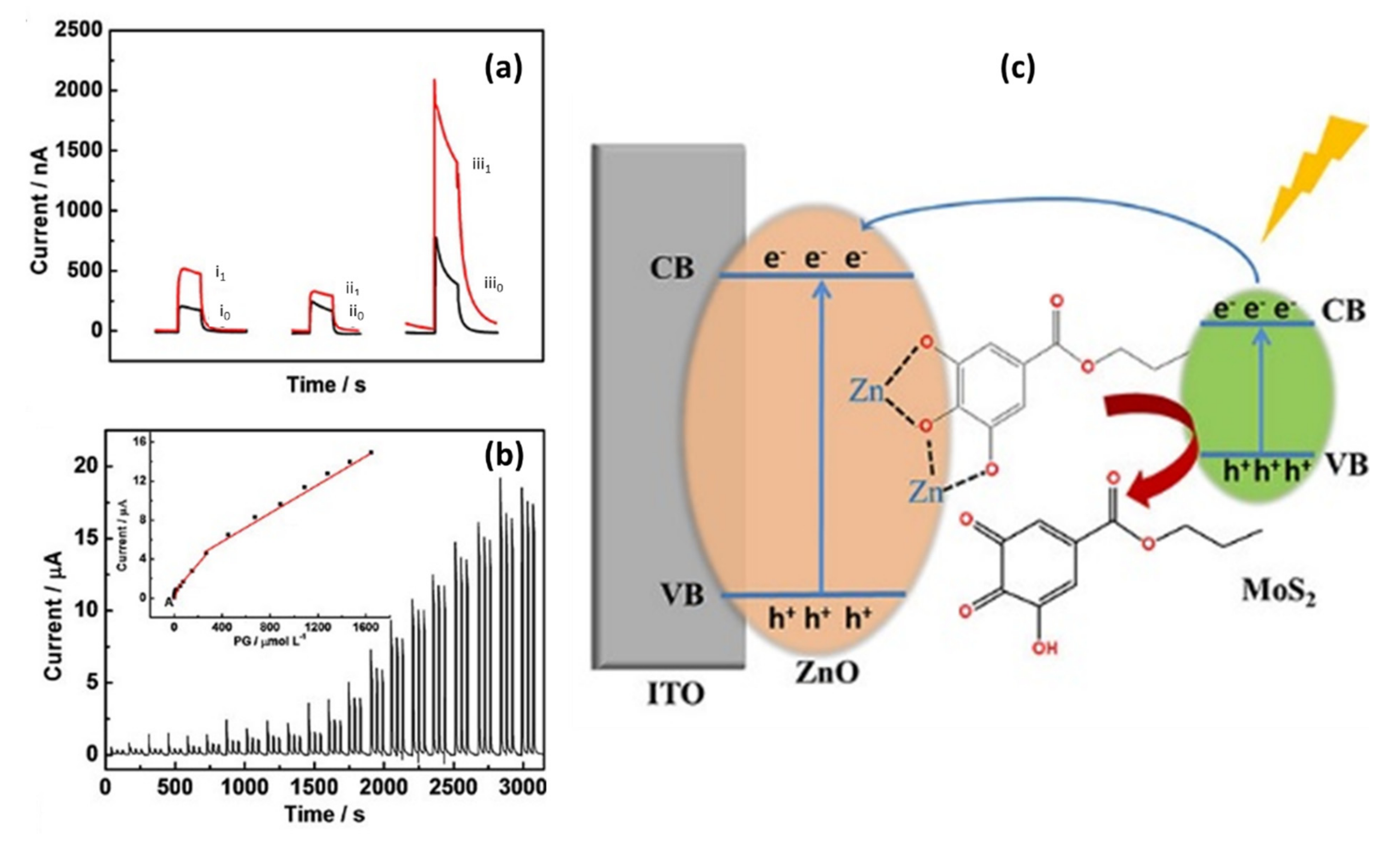
  232. Han, F.; Song, Z.; Nawaz, M.H.; Dai, M.; Han, D.; Han, L.; Fan, Y.; Xu, J.; Han, D.; Niu, L. MoS2/ZnO-Heterostructures-Based Label-Free, Visible-Light-Excited Photoelectrochemical Sensor for Sensitive and Selective Determination of Synthetic Antioxidant Propyl Gallate. Anal. Chem. 2019, 91, 10657–10662. [Google Scholar] [CrossRef]
  233. Jalali, M.; Moakhar, R.S.; Abdelfattah, T.; Filine, E.; Mahshid, S.S.; Mahshid, S. Nanopattern-Assisted Direct Growth of Peony-like 3D MoS2/Au Composite for Nonenzymatic Photoelectrochemical Sensing. ACS Appl. Mater. Interfaces 2020, 12, 7411–7422. [Google Scholar] [CrossRef]
  234. Çakıroğlu, B.; Özacar, M. A Photoelectrochemical Biosensor Fabricated Using Hierarchically Structured Gold Nanoparticle and MoS2 on Tannic Acid Templated Mesoporous TiO2. Electroanalysis 2020, 32, 166–177. [Google Scholar] [CrossRef]
  235. Fu, N.; Hu, Y.; Shi, S.; Ren, S.; Liu, W.; Su, S.; Zhao, B.; Weng, L.; Wang, L. Au Nanoparticles on Two-Dimensional MoS2 Nanosheets as a Photoanode for Efficient Photoelectrochemical MiRNA Detection. Analyst 2018, 143, 1705–1712. [Google Scholar] [CrossRef]
  236. Sun, J.; Sun, H.; Liang, Z. Nanomaterials in Electrochemiluminescence Sensors. ChemElectroChem 2017, 4, 1651–1662. [Google Scholar] [CrossRef] [Green Version]
  237. Ravalli, A.; Voccia, D.; Palchetti, I.; Marrazza, G. Electrochemical, Electrochemiluminescence, and Photoelectrochemical Aptamer-Based Nanostructured Sensors for Biomarker Analysis. Biosensors 2016, 6, 39. [Google Scholar] [CrossRef] [PubMed] [Green Version]
  238. Li, J.; Guo, S.; Wang, E. Recent Advances in New Luminescent Nanomaterials for Electrochemiluminescence Sensors. RSC Adv. 2012, 2, 3579–3586. [Google Scholar] [CrossRef]
  239. Chen, X.; Liu, Y.; Ma, Q. Recent Advances in Quantum Dot-Based Electrochemiluminescence Sensors. J. Mater. Chem. C 2018, 6, 942–959. [Google Scholar] [CrossRef]
  240. Francis, P.S.; Hogan, C.F. Chapter 13—Luminescence. In Advances in Flow Injection Analysis and Related Techniques; Kolev, S.D., Mckelvie, I.D., Eds.; Elsevier: Amsterdam, The Netherlands, 2008; Volume 54, pp. 343–373. [Google Scholar]
  241. Fu, X.-L.; Hou, F.; Liu, F.-R.; Ren, S.-W.; Cao, J.-T.; Liu, Y.-M. Electrochemiluminescence Energy Resonance Transfer in 2D/2D Heterostructured g-C3N4/MnO2 for Glutathione Detection. Biosens. Bioelectron. 2019, 129, 72–78. [Google Scholar] [CrossRef] [PubMed]
  242. Li, M.; Wang, C.; Chen, L.; Liu, D. A Novel Electrochemiluminescence Sensor Based on Resonance Energy Transfer System between Nitrogen Doped Graphene Quantum Dots and Boron Nitride Quantum Dots for Sensitive Detection of Folic Acid. Anal. Chim. Acta 2019, 1090, 57–63. [Google Scholar] [CrossRef]
  243. Zhang, W.; Xiong, H.; Chen, M.; Zhang, X.; Wang, S. Surface-Enhanced Molecularly Imprinted Electrochemiluminescence Sensor Based on Ru@SiO2 for Ultrasensitive Detection of Fumonisin B1. Biosens. Bioelectron. 2017, 96, 55–61. [Google Scholar] [CrossRef]
  244. Gan, X.; Zhao, H.; Quan, X. Two-Dimensional MoS2: A Promising Building Block for Biosensors. Biosens. Bioelectron. 2017, 89, 56–71. [Google Scholar] [CrossRef]
Figure 1. Schematic diagrams of (a) lithium intercalation exfoliation [44], (b) (i) exfoliation by sonication [48], (ii) exfoliation by high shear rate using a basic kitchen blender [50], (c) hydrothermal synthesis [54], (d) CVD method [56]. Figures reproduced with permission from Ref. [44], © 2014 WILEY-VCH Verlag GmbH & Co. KGaA, Weinheim, Germany, Refs. [48,50] copyright © 2015, American Chemical Society, Washington, DC, USA, Ref. [54] © 2018 Elsevier B.V., Amsterdam, The Netherlands. All rights reserved, Ref. [56] copyright © 2013, American Chemical Society.
Biosensors 12 00386 g001
Figure 2. TEM images of (a) MoS2-Au [69], (b) TTR-MoS2-Au [80], (c) MoS2-PEI-Au [81], (d) CuO-MoS2 [82] nanocomposites produced by ex situ functionalization. Figures reproduced with permission from Ref. [69] copyright © 2016 Elsevier B.V., Refs. [80,81] copyright © 2017 Elsevier B.V., Ref. [82] copyright 2020 Elsevier, Ltd. and Techna Group.
Biosensors 12 00386 g002
Figure 3. SEM image of (a) MoS2-Au [13], TEM images of (b) MoS2-MWCNT/Au [83], (c) MoS2-TiO2 [106], (d) MoS2-Cu2O/Pt, ((e) insert Pt NPs) [70], (f) N/F/MoS2-Ag [88], and (g) MoS2-PtPd ((h) insert SEM of MoS2-PtPd) [96], produced by in situ functionalization. Figures reproduced with permission from Ref. [13] copyright © 2016 American Chemical Society, Refs. [70,83] copyright © 2017 Elsevier B.V., Ref. [106] copyright © 2017 Published by Elsevier Ltd., ref. [88] copyright © 2018 Elsevier B.V., Ref. [96] copyright © 2019 Elsevier B.V.
Biosensors 12 00386 g003
Figure 4. (a) The band structures of MoS2 from bulk to monolayer MoS2 calculated at the DFT-PBE level. The horizontal dashed lines indicate the Fermi level. The arrows indicate the smallest value of the band gap (direct or indirect) for a given system. The green and blue lines represent the conduction and valence band edges, respectively [146]. (b) Structure of 2H- and 1T-MoS2 [46]. Figures reproduced with permission from Ref. [146] copyright © 2011 American Physical Society, and Ref. [46] copyright © 2011, American Chemical Society.
Biosensors 12 00386 g004
Figure 5. (a) EIS response of bare and modified electrodes with a frequency range from 0.01 to 100 kHz, with an amplitude of 5 mV. (b) The histogram for RCT of (i) bare/GCE, (ii) MoS2/GCE, (iii) Ag NPs-MoS2/GCE, (iv) Ag NPs-N-F-MoS2/GCE, (iii) AChE/CNTs-NH2/Ag NPs-N-F-MoS2/GCE. Error bars are coefficients of variation across three repetitive experiments. (c) CV response of bare and modified electrodes at a scan rate of 100 mV s−1 [88], (d) EIS and (e) CV responses of (i) bare/GCE, (ii) MoS2/GCE, (iii) Au-MoS2/GCE, (iv) Pd-MoS2/GCE, and (v) Au-Pd-MoS2/GCE [89]. Figures reproduced with permission from Ref. [88] copyright © 2018 Elsevier B.V, and Ref. [89] copyright © 2016 Elsevier B.V.
Biosensors 12 00386 g005
Figure 6. (a) UV–visible spectroscopy spectra of MoS2 layers [168], (b) PL spectra of MoS2 thin films with thicknesses ranging from 1.3 to 7.6 nm [46], (c) photoconductivity spectra for mono (red dots) and bilayer (green dots) MoS2 [144]. (d) Raman spectra for (top) bulk MoS2, and (bottom) 1L-MoS2 [167], (e) Raman spectra of MoS2 before (red) and after (blue) Ag NP decoration [161], (f) PL spectra of MoS2 decorated with Ag NPs [161]. Figures reproduced with permission from Ref. [168] copyright © 2017 Elsevier, Ltd., Refs. [46,144] copyright © 2011, American Chemical Society, Ref. [167] copyright 2019–2020 Aptara, Inc. and Ref. [161] rights managed by AIP Publishing, Woodbury, NY, USA.
Biosensors 12 00386 g006
Figure 7. (a) Schematic representation of PEC sensing with a traditional three-electrode system, (b) the photocurrent generation mechanism, [173], and (c) schematic representation showing the general principles of ECL [184]. Figure reproduced with permission from Ref. [173] copyright © 2020 American Chemical Society, Ref. [184] copyright © 2007 Elsevier B.V.
Biosensors 12 00386 g007
Figure 8. (a) CV response of bare and modified gold electrodes in 1 mM ferrocene carboxylic acid and 0.1 M PBS at 50 mV/s vs. Ag/AgCl reference electrode. (b) Amperometric responses of modified gold electrodes for the sensing of glucose concentration in the range from 0.25 to 13.2 mM at + 0.35 V applied potential. (c) Schematic representation of Au NPs decorated on a MoS2 interface and a reaction mechanism on MoS2-AuNPs-GOx composite [69]. Figures reproduced with permission from Ref. [69], copyright © 2016 Elsevier B.V.
Biosensors 12 00386 g008
Figure 9. (a) Schematic representation of the PtW-MoS2 nanocomposite sensor for the detection of H2O2 released from living cells (AA: ascorbic acid, UA: uric acid). (b) EIS response of bare and modified electrodes in a solution containing 0.1 M KCl and 2 mM Fe(CN)63−-Fe(CN)64−. The equivalent circuit used to fit the Nyquist plots obtained from modified electrodes is shown in inset. (c) CV responses of PtW-MoS2 nanocomposite in the absence and presence of 0.05 mM H2O2 in 0.1 M PBS (pH = 7.4) [94]. Figures reproduced with permission from Ref. [94], copyright © 2016 Elsevier B.V.
Biosensors 12 00386 g009
Figure 10. (a) Schematic representation of PtPd-MoS2 for the detection of HBs Ag and signal response mechanism. (b) Amperometric response: (curve i) MoS2, (curve ii) PtPd NCs, (curve iii) PtPd-MoS2 in 10 mL PBS (pH = 7.38). (c) DPV responses of different concentrations of HBs Ag ranging from (curve i) 32 fg/mL to (curve xi) 100 ng/mL [96]. Figures reproduced with permission from Ref. [96], copyright © 2019 Elsevier B.V.
Biosensors 12 00386 g010
Figure 11. (a) Schematic representation of MoS2-Au-based immunosensor for CEA detection and signal response mechanism. (b) CV and (c) EIS curves of (i) bare GCE, modified GCE (ii) MoS2-Au, (iii) anti-CEA/MoS2-Au, (iv) BSA/anti-CEA/MoS2-Au, (v) CEA/BSA/anti-CEA/MoS2-Au and (vi) CEA/BSA/anti-CEA/MoS2-Au by using [Fe(CN)6]3-/4- as an electrochemical indicator, respectively. CV responses of the proposed “sandwich” immunosensor formation with different electrodes (d) HRP-anti-CEA, (e) HRP-anti-CEA/Au, (f) BSA/HRP-anti-CEA/MoS2-Au, and (g) HRP/HRP-anti-CEA/MoS2-Au in 0.1 M PBS (i) in the absence and (ii) presence of 0.01 M o-PD + 0.16 M H2O2 [220]. Figures reproduced with permission from Ref. [220], copyright © 2019 Elsevier B.V.
Biosensors 12 00386 g011
Figure 12. (a) Schematic representation of MoS2-TiO2-GOxǀITO PEC biosensor, the energy diagram and the proposed charge transfer mechanism. (b) Photocurrent response of (i) Pure MoS2|ITO, (ii) TiO2 nanorods|ITO, (iii) MoS2-TiO2|ITO, (iv) MoS2-TiO2-GOx|ITO in PBS solution (pH 7.4). CV of (c) TiO2-GOx, (d) MoS2-Gox, and (e) MoS2-TiO2-GOx (i) without and (ii) with illumination in PBS solution containing 2 mM glucose [106]. Figures reproduced with permission from Ref. [106], copyright © 2017 Published by Elsevier, Ltd.
Biosensors 12 00386 g012
Figure 13. (a) Photocurrent responses of ZnO (curves i0 and i1), MoS2 (curves ii0 and ii1), and MoS2-ZnO (curves iii0 and iii1)-modified ITO electrodes in the absence of (curves i0, ii0, and iii0) and presence of (curves i1, ii1, and iii1) 12.43 μmol L−1 PG. (b) Photocurrent responses of MoS2-ZnO-modified ITO electrodes upon different concentrations of PG. The inset is the corresponding linear calibration curve. (c) Proposed mechanism of the MoS2-ZnO-based PEC sensor for the detection of PG [232]. Figures reproduced with permission from Ref. [232], copyright © 2019, American Chemical Society.
Biosensors 12 00386 g013
Figure 14. Schematic representation of the proposed immunosensor. (a) Formation of MoS2-PEI-Au nanocomposites and (b) the preparation procedure of the luminol-Au@BSA-Ab2 bioconjugation. (c) ECL profiles of the immunosensor before and after incubation with luminol-Au@BSA-Ab2 bioconjugate in 0.01 M pH 7.4 PBS containing 3 mM H2O2 and 10 ng/mL AFP. (d) ECL responses for AFP detection. The concentrations of AFP (ng/mL): (i) 0.0001, (ii) 0.001, (iii) 0.01, (iv) 0.1, (v) 1, (vi) 10, (vii) 100, and (viii) 200 (inset: calibration curve) [81]. Figures reproduced with permission from Ref., copyright © 2017 Elsevier B.V.
Biosensors 12 00386 g014
Table 1. Functionalization methods of MoS2 nanosheets with different metal and metal oxide NSs and their applications in electrochemical sensors.
MoS2-NS Composites Method of FunctionalizationMetal and Metal Oxides Structural MorphologySize (Diameter)Type of SensorRef.
Ex situ functionalizationMoS2-AuPost immobilizationNanoparticles5 nmElectrochemical biosensor[69]
TTR-MoS2-AuPost immobilizationNanocrystals-Photoelectrochemical immunosensor[80]
MoS2-PEI-AuPost immobilizationNanoparticles12 nmElectrochemiluminescence immunosensor[81]
CuO-MoS2Post immobilizationNanotubes20 nmElectrochemical sensor[82]
In situ functionalizationMoS2-AuElectrodepositionNanoparticles 10 mElectrochemical aptasensor[13]
MoS2-MWCNT/AuElectrodepositionNanoparticles3–5 nmElectrochemical sensor[83]
MoS2-Au/PtElectrodepositionNanoparticles100 nmElectrochemical biosensor[84]
Cu-MoS2ElectrodepositionNanoflowers-Electrochemical biosensor[85]
ZnO-MoS2ElectrodepositionNanosheets50 nmElectrochemical sensor[86]
Ni-MoS2-NafChemical reductionNanoparticles6 nmElectrochemical sensor[35]
Au-MoS2Chemical reductionNanoparticles80 nmElectrochemical sensor[87]
N/F/MoS2-AgChemical reductionNanoparticles3 nmElectrochemical sensor[88]
Au-Pd/MoS2Chemical reductionNanoparticles-Electrochemical sensor[89]
TiO2-MoS2-AuChemical reductionNanoparticles5–10 nmPhotoelectrochemical aptasensor[90]
Pt-MoS2Chemical reductionNanoparticles2.5 nmElectrochemical biosensor[91]
PtNi-MoS2Chemical reductionNanoparticles1.35–6.26 nmElectrochemical sensor[92]
Cu2O-MoS2Chemical reductionNanoparticles6–18 nmElectrochemical sensor[93]
PtW-MoS2Chemical reductionNanocubes10 nmElectrochemical sensor[94]
Pd–MoS2Chemical reductionNanoparticles-Electrochemical aptasensor[95]
PtPd-MoS2Chemical reductionNanocubes50 nmElectrochemical immunosensor[96]
Pt-MoS2Chemical reductionNanoparticles-Electrochemical sensor[97]
Ag-MoS2Chemical reductionNanoparticles5 nmElectrochemical sensor[98]
MoS2-PtChemical reductionClover-like nanoparticles15.3–2 nmElectrochemical sensor[99]
Au−Pd−Pt/MoS2Chemical reductionNanoflowers14–26 nmElectrochemical sensor[100]
PdNi-MoS2Chemical reductionNanowires0.5–3 nmElectrochemical sensor[101]
MoS2-Cu2O-AuHydrothermal reactionNanocrystals20–30 nmElectrochemical immunosensor[102]
NiO-MoS2Hydrothermal reactionNanoparticles38–72 nmElectrochemical sensor[103]
Fe2O3-MoS2Hydrothermal reactionNanoflowers-Electrochemical sensor[104]
Fe3O4-MoS2Hydrothermal reactionNanospheres20–30 nmElectrochemical sensor[105]
MoS2-TiO2Hydrothermal reactionNanorods20 nmPhotoelectrochemical biosensing[106]
Ag/MoS2@Fe3O4Hydrothermal reactionNanospheres50 nmElectrochemical immunosensor[107]
MoS2-Cu2O/PtSolvothermal reactionNanoparticles15 and 3 nmElectrochemical immunosensor[70]
Cu-MoS2-NafSolvothermal reactionNanoparticles1–5 nmElectrochemical sensor[108]
NiCo2O4-MoS2Solvothermal reactionNanorods-Electrochemical sensor[109]
TTR; transthyretin, PEI; polyethylenimine, CuO; copper oxide, MWCNT; multiwalled carbon nanotubes, Cu2O; cuprous oxide, Cu; copper, ZnO; zinc oxide, Naf; Nafion, N/F; nitrogen fluorine, TiO2; titanium dioxide, PtW; platinum/tungsten, NiO; nickel oxide, Fe2O3, Fe3O4; iron (II, III) oxide, NiCo2O4; nickel cobaltite.
Table 2. Electrochemical biosensors based on 2D-MoS2/metal-NSs composites.
SensorAnalyteElectrochemical MethodLinear RangeLODRef.
Au-MoS2/GCEATP
Thrombin
SWV1 nM–10 mM
0.01 nM–10 µM
0.32 nM
0.0014 nM
[13]
GCE/Ni-MoS2/NafGlucoseAmperometry0–4 mM0.31 M[35]
MoS2/Au/GOxGlucoseAmperometry0.25–13.2 mM0.042 µM[69]
CuO/MoS2/GCEGlucoseAmperometry35–800 μM0.017 μM[82]
MoS2−Au/Pt@GCEH2O2Amperometry10 μM–19.07 mM0.39 μM[84]
Cu-MoS2/GCEH2O2
glucose
Amperometry0.04–35.6 μM
1–70 μM
0.021 μM
0.32 μM
[85]
ZnO/MoS2/GCEDNADPV1.0 fM–1.0 µM0.66 fM[86]
Au@MoS2/GCEAA
DA
UA
DPV20–300 µmol/L
5–200 µmol/L
20–400 µmol/L
3.0 µmol/L
1.0 µmol/L
5.0 µmol/L
[87]
Au-Pd/MoS2/GCEH2O2
Glucose
DPV
Amperometry
0.8 µM–10 Mm
0.5–20 mM
0.16 µM
0.40 mM
[89]
Pt-MoS2/GCEH2O2Amperometry0.004–48.5 mM0.001 mM[91]
PtNi@MoS2/GCEDA
UA
DPV0.5–250 µM
0.5–1800 µM
0.1 µM
0.1 µM
[92]
Cu2O/MoS2/GCEGlucoseAmperometry0.01–4.0 mM1.0 µM[93]
PtW/MoS2/GCEH2O2Chronoamperometry1 μM–0.2 mM5 nM[94]
Pd/PDDA–G–MoS2/GCETBDPV0.0001–40 nM0.062 pM[95]
PtNPs@MoS2/GCEDA
UA
DPV0.5–150 μmol/L
5–1000 μmol/L
0.12 μmol/L
0.8 μmol/L
[97]
Ag@MoS2/GCEDADPV1−500 μM0.2 μM[98]
MoS2-CPtNPs/GCEDA
UA
DPV5–200 µΜ
20–500 μM
0.39 μM
1.8 μM
[99]
Laminin/Au−Pd−Pt/MoS2/SPCEH2O2Amperometry1–100 nM0.3 nM[100]
NiO/MoS2/GCEGlucoseAmperometry0.01–10 mM1.62 μM[103]
GCE/Cu-MoS2/NafionGlucoseAmperometry0–4 mM-[108]
NiCo2O4-MoS2/chitosan/GCEGlucoseAmperometry0.0007–13.78 mM0.23 µM[109]
MoS2-PPY-AuNPs/GCEGlucoseDPV0.1–80 nM0.08 nM[206]
AuNPs@MoS2/GCEmiRNA-21DPV10 fM–1 nM0.78 fM[208]
Chox/MoS2-AuNPs/GCECholesterolAmperometry0.5–48 μM0.26 ± 0.015 μM[209]
MoS2-Au-PEI-heminClenbuterol (CLB)DPV10 ng/mL–2 μg/mL1.92 ng/mL[210]
NF/AuNPs/CuO-MoS2GlucoseChronoamperometry0.5 μM–5.67 mΜ0.5 μM[211]
MCH/dsDNA/MoS2-AuNPs/GCET4 polynucleotide kinase
(PNK)
SWV0.001–10 U/mL2.18 × 10−4 U/mL[212]
miRNA/MCH/SH-RNA/AuNPs-MoS2/FTOMicroRNA-155DPV1 fM–10 nM0.32 fM[213]
ATP; triphosphate, DA; dopamine, DNA; deoxyribonucleic acid, DPV; differential pulse voltammetry, SWV; square Wave Voltammetry, PDDA–G; poly(diallyldimethylammonium chloride)–graphene, TB; thrombin, CPtNPs; Clover-like platinum nanoparticle, PPY; polypyrrole, miRNA-21; microribonucleic acid-21, Chox; cholesterol oxidase, NF; Nafion, MCH; 6-mercaptohexanol, FTO; fluorine doped tin oxide.
Table 3. Electrochemical immunosensors based on 2D-MoS2/metal-NSs composites.
SensorAnalyteElectrochemical MethodLinear RangeLODRef.
MoS2@Cu2O-Pt/Ab2hepatitis B antigenAmperometry0.5 pg/mL–200 ng/mL0.15 pg/mL[70]
BSA/anti-HBs/PtPd NCs@MoS2/
GCE
Hepatitis B antigenDPV32 fg/mL–100 ng/mL10.2 fg/mL[96]
MoS2@Cu2O-Au-Ab2Alpha fetoprotein (AFP)Amperometry0.1 pg/mL–50 ng/mL0.037 pg/mL[102]
Ab2-Ag/MoS2@Fe3O4/MGCEcarcinoembryonic antigen (CEA)DPV0.0001–20 ng/mL0.03 pg/mL[107]
HRP/HRP-anti-CEA/MoS2-AuNPscarcinoembryonic antigen (CEA)DPV10 fg/mL–1 ng/mL1.2 fg/mL[220]
GCE/MoS2-Au-Ab1CEADPV1 pg/mL–50 ng/mL0.27 pg/mL[221]
Pd NPs@MoS2/NiCoProcalcitonin Chronoamperometry0.001–50 ng/mL0.36 pg/mL[222]
Au-MoS2/ITOTriiodothyronine (T3) EIS0.01–100 ng/mL2.5 pg/mL[223]
Cu-MoS2/GCE3-phenoxybenzoic acid (3-PBA),EIS0–6 µg/mL3.8 µM[224]
Tac/BSA/Ab/PS-AuNRs@L-Cys-MoS2/GCETacrolimus (Tac)DPV1.0–30 ng/mL0.17 ng/mL[225]
Ab1; primary antibody, Ab2; secondary antibody, HBs Ag; Hepatitis B surface antigen, BSA; bovine serum albumin, ITO; indium tin oxide, L-Cys; L-cysteine, PS-AuNRs; polystyrene-gold nanorods.
Table 4. Photoelectrochemical sensors based on 2D-MoS2/metal-NSs composites.
SensorAnalyteLinear RangeLODRef.
TTR/AuCNs/MoS2/GCETetrabromobisphenol A0.1 nM−1.0 µM.0.045 nM[80]
BSA|aptamer|TiO2-MoS2-AuNP|ITOkanamycin0.2 nM−450 nM0.05 nM[90]
GOx|MoS2-TiO2|ITOGlucose 0.1−10.5 mM0.015 mM[106]
MoS2-ZnO|ITOPropyl gallate0.1249−1643 μmol/L1.2 × 10−8 mol/L[232]
Au/MoS2/TiO2Glucose5−1000 μM1.3 nM[233]
Pro-GRP-MIP/AuNPs/2D-MoS2/GCEPro-gastrin-releasing peptide (Pro-GRP) 0.02–5 ng/mL0.0032 ng/mL[177]
Au-MoS2/FTOanti-human IgG41.7 nM–4.17 μM4.17 nM[178]
ITO/MTiO2-AuNPs-MoS2-GOxGlucose 0.004–1.75  mM1.2  μM[234]
biotin DNA/MoS2-AuNPs/ITOmiRNA10 fM–1 nM4.21 fM[235]
MIP; molecularly imprinted polymer.
Table 5. Electrochemiluminescence sensors based on 2D-MoS2/metal-NSs composites.
SensorAnalyteLinear RangeLODRef.
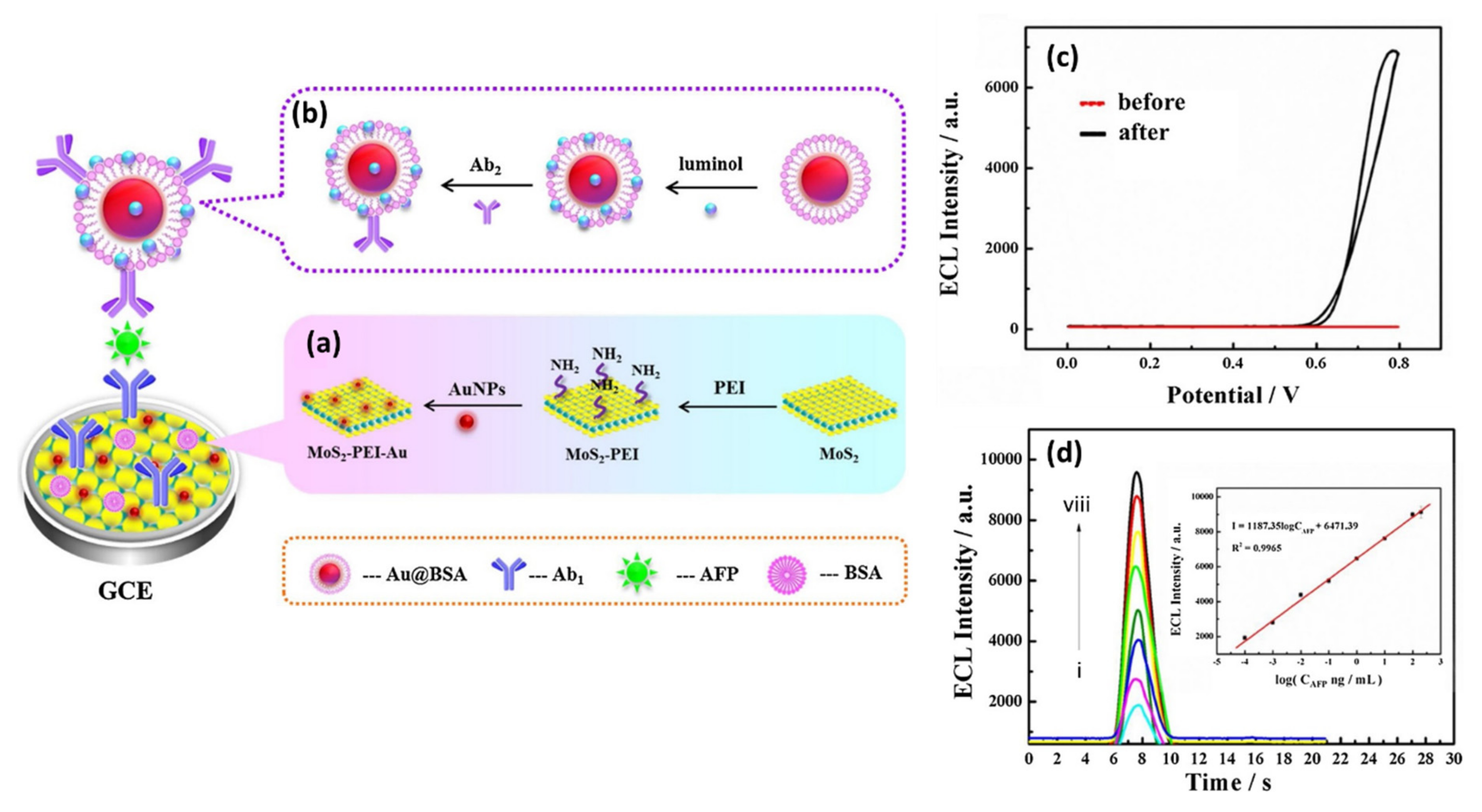
luminol-Au@BSA-Ab2/AFP/BSAT/Ab1/Chi/MoS2-PEI-Au/GCE.Alpha fetal protein (AFP),0.0001−200.0 ng/mL1.0 × 10−5 ng/mL[81]
BSA/Ab2/ABEI-Cys/Au–Pd–Pt/MoS2cystatin C (CYSC)1.0 fg/mL−5.0 ng/mL0.35 fg/mL[186]
QDs–Apt2/PDGF-BB/Apt1/MoS2–AuNPs/GCEplatelet-derived growth factor-BB0.01−100 pmol/L1.1 fmol/L[187]
ABEI; N-(aminobutyl)-N-(ethylisoluminol), PDGF-BB; platelet-derived growth factor BB, QDs; quantum dots.
Publisher’s Note: MDPI stays neutral with regard to jurisdictional claims in published maps and institutional affiliations.

