Spintronics [
1] is a promising research field that focuses on electrons in a degree of freedom (i.e., spin). Conventional electronic devices have high power consumption and a relatively low circuit integration, resulting in physical limitations. Generally, spintronics strives for ultra-efficient and ultra-fast devices [
2,
3,
4,
5]. Thus, the development of corresponding spintronic materials is crucial and must be realized. For the past several years, diluted magnetic semiconductors [
6], half-metals [
7], and topological insulators [
8] were proposed, and while they can each meet various requirements of spintronics, they cannot meet all of them.
In 2008, Wang [
2] proposed a new spintronic material—spin-gapless semiconductors (SGSs) [
9]. In general, SGSs possess a gapless feature in one spin channel and a semiconducting gap in the other spin channel. In terms of differences in the dispersion of its band structures near the Fermi level, SGSs can be divided further into parabolic or Dirac-like crossing types. Parabolic SGSs show a quadratic band dispersion for gapless bands, while Dirac-like crossing SGSs (DSGSs) exhibit a linear band dispersion at the Fermi level in one spin channel. Due to this unique dispersion, the effective electron quantity can be eliminated in DSGSs. As a member of the topological non-trivial family, DSGSs have 100% spin polarization, high Fermi velocity (
vF), massless fermions around the Fermi level, and no dissipation characteristics. These desirable characteristics indicate possible applications in future high efficiency spintronic devices.
In the past (and based on first-principle calculations), DSGSs with a single Dirac-like crossing could be observed in two-dimensional Ni
2C
24S
6H
12 [
10] and Mn
2C
6S
12 [
11] metal–organic frameworks as well as NiCl
3 [
12], MnX
3 (X = F, Cl, Br, and I) [
13] and YN
2 monolayers [
14]. DSGSs with more than two Dirac-like crossings can be found in CrO
2/TiO
2 heterostructures [
15] and three-dimensional MnF
3 materials [
16]. Compared with DSGSs that have a single Dirac-like crossing, DSGSs with multiple Dirac band dispersions have a stronger nonlinear electromagnetic response and a higher carrier transport efficiency at the Fermi level.
In this study, we proposed a new rhombohedral-type of bulk material, PdF
3, which demonstrates the spin-gapless semiconducting feature with multiple linear band dispersions, by means of the density functional theory (DFT) method. We should point out that this material with
has been prepared by the reaction of dry fluorine on PdI
2 at about 400 °C [
17]. Its magnetism and physical stability under the spin-orbit coupling effect and mechanic pressure was also investigated in detail. Additionally, we built a PdF
3/Ga
2O
3/PdF
3 magnetic tunnel junction (MTJ) and investigated its nonequilibrium spin injection and spin-polarized quantum transport properties based on the non-equilibrium Green’s function (NEGF) and in combination with first-principles calculations. The results showed that the MTJ exhibits a perfect spin-filtering feature with extremely high magnetoresistance. Details about the computational and simulation models can be found in the
supplementary materials (Supplementary Figures S1 and S2).
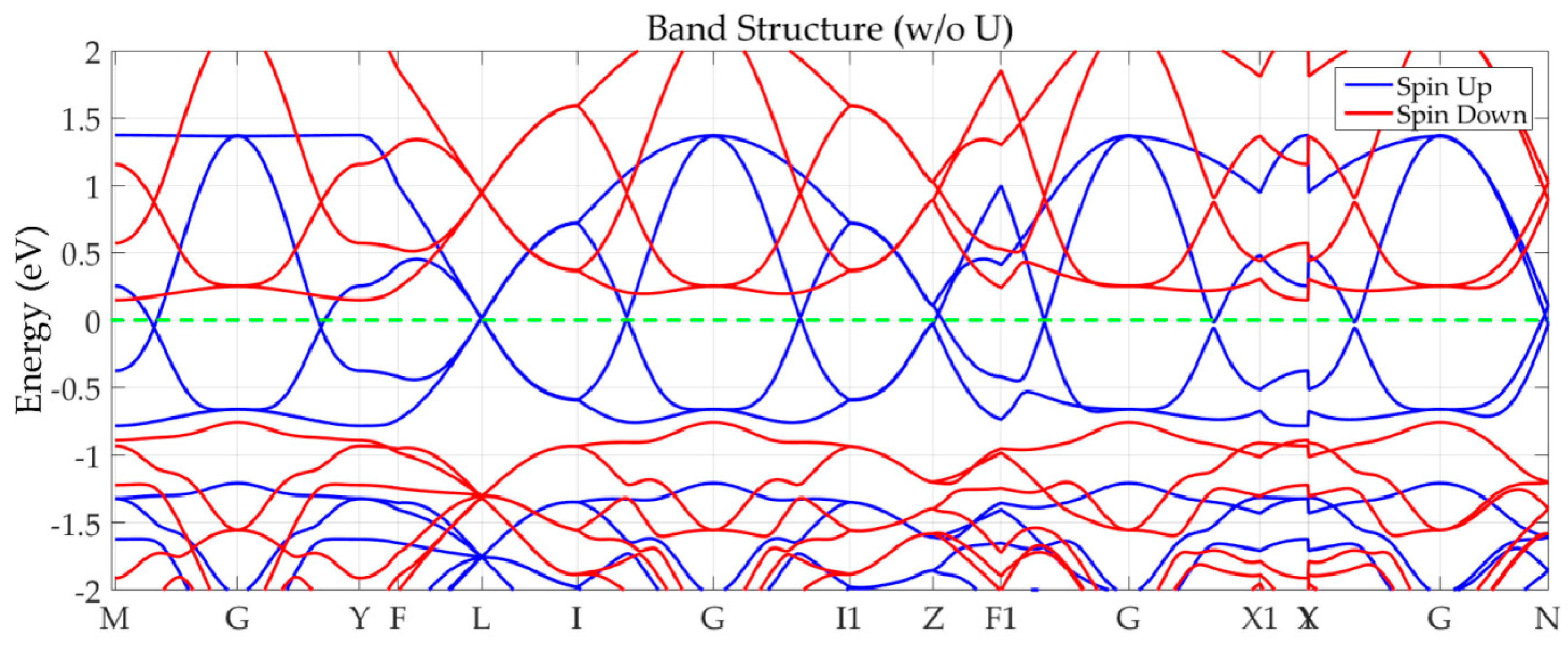
The electronic structures of bulk PdF
3 were calculated without the effect of spin-orbit coupling (
Figure 1). We found that its electronic structure shows multiple spin-gapless semiconducting features with linear dispersion, which indicates excitation at the Fermi level owning the dissipationless and massless features. Considering that the correlation effect from the 4
d orbit of a Pd element cannot be regarded, we also adapted DFT plus U to conduct this calculation. In this study, several Hubbard U values (from 0 to 4 eV) were tested on-site for Pd-4
d orbits. The corresponding band structures (
Supplementary Figure S3) were not significantly different from the gapless spin-up structures, and the enlargement of the gap in the spin-down channel stabilized the semiconducting feature. Therefore, we will focus on the Perdew−Burke−Ernzerhof (PBE) results in the following discussion. Also, the modified Becke–Johnson exchange potential with the generalized gradient approximation (GGA) method was also used in this work to examine the electronic structure of PdF
3 bulk and the results are shown in
Supplementary Figure S4.
As shown in
Figure 1, there is clearly a semiconducting gap at about 0.92 eV in the spin-down channel, and a gapless configuration in the spin-up channel. In total, ten linear band crosses appear exactly at the Fermi level. Some of these linear crosses are located at the high symmetry points (one at the L point and another near the Z point along the Z–F1 line), and some appear along the high symmetry lines (M–G, G–Y, I–G, G–I1, F1–G, G–X1, Y|X–G, and G–N lines respectively). Also, one can see that the crossing bands have a very large linear energy range (up to 1 eV). As was the case with bulk ReO
2 [
18], hourglass-shaped band dispersions are apparent along the Z–F
1 and G–N lines. Such an irregular distribution of band crosses and linear SGS features bring the anisotropy, but high Fermi velocities, in the whole Brillouin zone. Considering the rotation symmetry of the Brillouin zone, these linear crosses will form the Dirac rings and induce a more intensive nonlinear electromagnetic response than that induced by other materials containing a single Dirac cone. Moreover, a higher efficiency of carrier transport will exist at the Fermi level via the multiple crosses.
As shown in
Figure 2, we computed the spin-resolved total density of states (TDOS) and partial density of states (PDOS) spectra. From the TDOS, a valley can be seen at the Fermi level in the spin-up channel, and the major distribution of spin-down states is below −0.7 eV and above 0.2 eV, thus forming a semiconducting gap. The spin-polarization rate [
19] can be obtained by
, where
represents the states of the spin-up or spin-down channels near the Fermi level. Here,
P is 100%. In PDOS, the electronic structures near the Fermi level are dominated by the
p-d hybridization between Pd and F atoms.
To calculate the effect of spin-orbit coupling, we examined the band structures (
Supplementary Figure S5). As shown in this figure, the impact of SOC on these linear band crosses of PdF
3 was very weak. Meanwhile, we considered the uniform strain effect to examine the band structural stability of PdF
3 (
Supplementary Figure S6). It was apparent that as stress is applied, some linear crossings (such as the gapless crossings along I–I
1 under 8 GPa) are opened. In general, the characteristics of the spin-gapless behaviors in the spin-up channel still exist for PdF
3 based on our calculated band structures.
Due to the large band gap, Ga
2O
3 is one of the materials that have received significant attention in recent years [
20]. Further, the lattice mismatch between PdF
3 and Ga
2O
3 is less than 5%, and therefore, in this work, we built a PdF
3/Ga
2O
3/PdF
3 magnetic tunnel junction (MTJ) to conduct the corresponding spin-transport calculation (
Supplementary Figure S2).
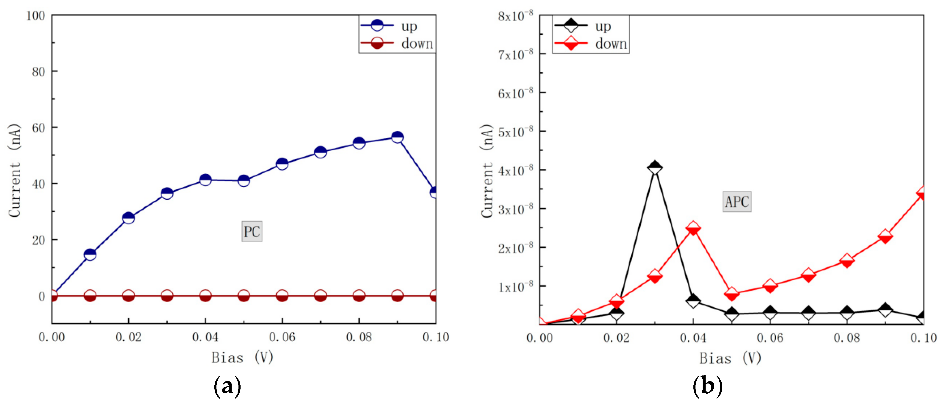
Figure 3 presents the calculated current–voltage curves of the MTJ in the parallel magnetization configuration (PC) and the antiparallel magnetization configuration (APC) between two electrodes. For PC, only the spin-up current contributes to the total spin-current in the range of considered bias voltage (from 0.0 to 0.1 V), and the spin-down current is strongly inhibited. In summary, the spin-up current increased rapidly when accompanied by an increase in bias voltage, while the turning decreased after the bias voltage increased up to 0.09 V. For APC, it does not matter if the spin-up and spin-down currents are both blocked.
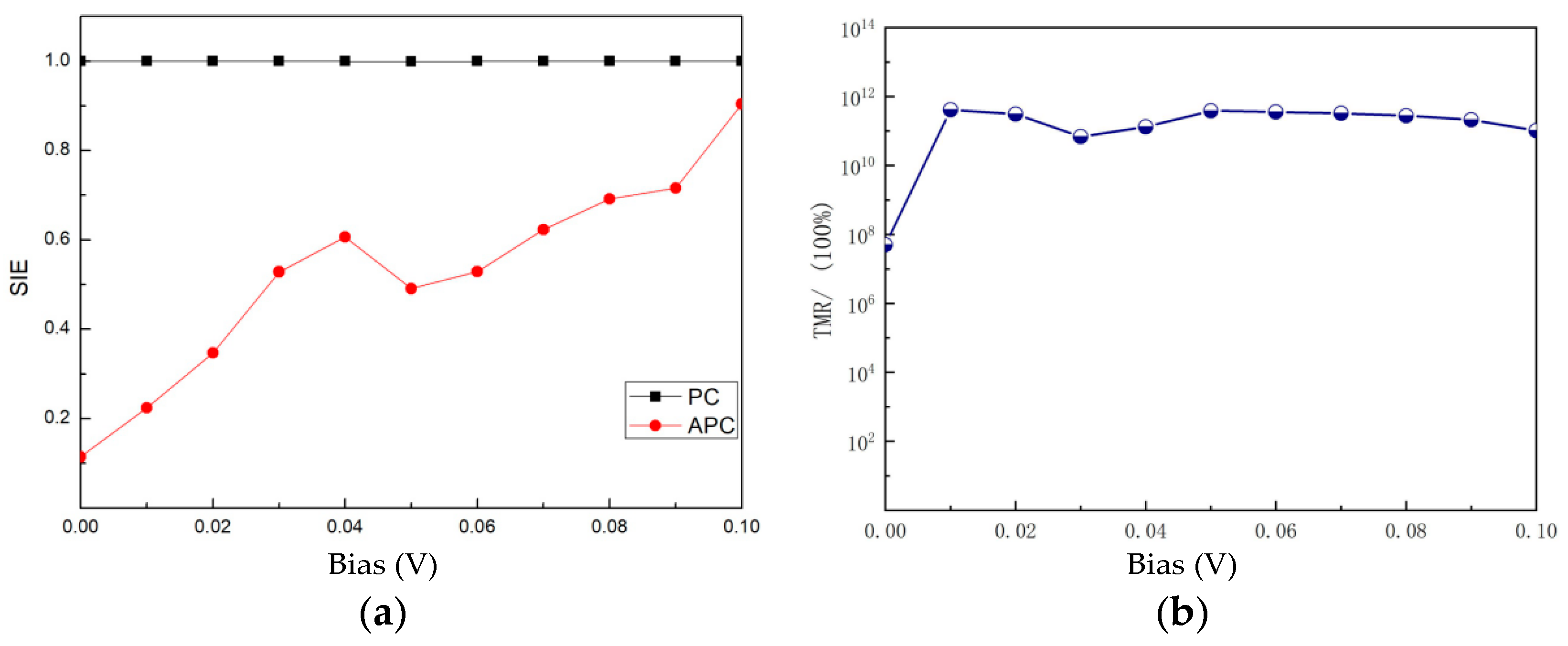
From the results of the spin-dependent current for PC and APC, the bias-voltage-dependent spin-injection efficiency (SIE) [
21] can be obtained by
, as shown in
Figure 4a. In PC, SIE maintains 100% consistently. This can be attributed to the electronic structures of the two electrodes; the spin-down gap blocks the leap of carriers, thus making
Idown vanishingly small. In APC, SIE at an equilibrium state is about 10% rather than 0% due to the broken mirror symmetry of this MTJ. When the bias voltage is applied, SIE increases to nearly 90%. Moreover, the fluctuation of
Iup/down notably causes a decrease in SIE at the range of bias voltage from 0.4 V to 0.5 V.
In our study, a tunnel magnetoresistance (TMR) ratio [
21] under finite bias is defined as
.
Figure 4b exhibits the TMR ratio versus bias voltage under equilibrium and nonequilibrium states. Here, for a PdF
3/Ga
2O
3/PdF
3 MTJ, the obtained equilibrium state TMR is about 5.04 × 10
7%, while the nonequilibrium state TMR is in the order of magnitudes of 10
11%. Also shown in
Figure 4b is the calculated TMR of about 4.11 × 10
11% at a bias of 0.01 V. Most importantly, the high TMR in this MTJ is very stable in the range of bias voltage variation from 0.01 V to 0.1 V.
To further understand the equilibrium state of the TMR, the transmission coefficient as a function of electron energy at a finite bias voltage range is shown in
Supplementary Figure S7. In PC, results reveal that the transmission coefficient of spin-up electrons at the Fermi level is much higher than that of spin-down electrons, showing that the major contribution of current comes from the spin-up electrons. In APC, the transmission coefficients of both spin-up and spin-down electrons are almost equal and vanishingly small, inducing an imperceptible current compared with that in PC. In summary, the transmission coefficient in APC is much smaller than that in PC, so an extremely high TMR can be obtained.
Furthermore, we calculated the nonequilibrium transmission spectrum
. It is worth noting that the aforementioned spin-polarized current is obtained according to integral transmission coefficients at the bias voltage window of
which is to say,
Supplementary Figure S8 shows the nonequilibrium transmission spectrum under the bias voltage value of 20 mV, 40 mV, 60 mV, and 80 mV, respectively. One can see that the PC transmission curves within the bias window have not changed much. Also, the APC is still much lower than the PC within the bias window; therefore, an ultra-high TMR ratio can be maintained under a broad range of bias. Meanwhile, due to the enhancement of the broken geometric symmetry of this MTJ, the increased bias voltage will intensify the division of transmission curves in APC. Moreover, there is an obvious decrease in the spin-up curve in APC within the bias voltage window, while the spin-down curve is not affected. This induces a rapid increase in spin-injection efficiency, with bias voltage increasing.
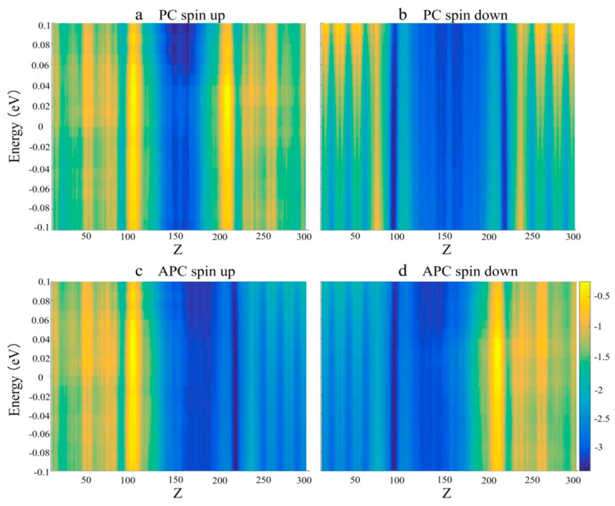
Finally, as shown in
Figure 5, the local density of states (LDOS) of this MTJ was calculated and summed up along the
z-axis. The insulating gap of Ga
2O
3 results in a central barrier without density of states.
Figure 5a demonstrates that in PC, the spin-up direction is free, and several spin-up electrons are able to tunnel in the central scattering zone from the left electrode and into the right electrode, indicating the formation of a transport channel. Therefore, the spin-up channel is in a majority spin state. As shown in
Figure 5b, there are few densities of states in the two electrodes in the spin-down channel. In other words, the spin-down channel is suppressed (minority spin state), and the spin-down electrons are difficult to transmit via the magnetic electrode by tunneling through the Ga
2O
3 barrier.
Figure 5c shows that in the APC spin-up channel, the density of states is mainly localized in the left electrode, while almost no density of states can be found in the right electrode. An explanation for this is that although the left electrode can generate spin-up electrons, there are few states in the right electrode that can accommodate these electrons; therefore, spin electrons cannot flow into the right electrode. On the contrary, in the APC spin-down channel (
Figure 5d), the density of states is concentrated on the right electrode, while there is little density of states in the left electrode. This shows that although the right electrode can accept a large number of electrons, the left electrode does not provide many electrons in the spin-down channel. Therefore, when this MTJ is in the APC state, both the spin-up and spin-down channels are blocked and the spin-polarized current cannot be detected; this resulted in a high resistance state.
To summarize, we theoretically proposed a new spintronic material, rhombohedral-type PdF3, which has fully spin-polarized and multiple linear spin-gapless semiconducting features. The computed results reveal the robustness of its innovative electronic structures and a long spin-coherence length. These excellent features show great promise for future experimental study and realistic application. We further built the PdF3/Ga2O3/PdF3 MTJ to deeply investigate the spin-transport feature by first-principles combined with the nonequilibrium Green’s function method. The ultrahigh equilibrium and nonequilibrium states of TMR are obtained at about 5.04 × 10⁷% and 4.11 × 10¹¹% (at 0.01 V), respectively. Additionally, the calculation of spin-injection efficiency exhibited the perfect spin-filtering performance of this MTJ. We also utilized the current–voltage curve, transmission spectrum, and local density of states to gain a deep understanding of the physical mechanism of its spin-transport properties. In conclusion, such an MTJ is a promising candidate for realistic spintronic applications. We hope this work can provide guidance for future experimental studies.

 ,
, 
