Article

Tunable Graphene-Based Plasmon-Induced Transparency Based on Edge Mode in the Mid-Infrared Region

1
College of Liberal Arts and Sciences, National University of Defense Technology, Changsha 410072, China
2
College of Physics and Electronics, Hunan University, Changsha 410006, China
*
Authors to whom correspondence should be addressed.
Nanomaterials 2019, 9(3), 448; https://doi.org/10.3390/nano9030448
Submission received: 11 February 2019 / Revised: 13 March 2019 / Accepted: 13 March 2019 / Published: 17 March 2019
(This article belongs to the Special Issue Graphene-Based Nanostructures and Optoelectronic Applications)

Abstract

:
A monolayer-graphene-based concentric-double-rings (CDR) structure is reported to achieve broadband plasmon-induced transparency (PIT) on the strength of edge mode in the mid-infrared regime. The theoretical analysis and simulation results reveal that the structure designed here has two plasmonic resonance peaks at 39.1 and 55.4 THz, and a transparency window with high transmission amplitude at the frequency of 44.1 THz. Based on the edge mode coupling between neighbor graphene ribbons, PIT phenomenon is produced through the interference between different (bright and dark) modes. The frequency and bandwidth of the transparency window and slow light time could be effectively adjusted and controlled via changing geometrical parameters of graphene or applying different gate voltages. Additionally, this structure is insensitive to the polarization and incident angle. This work has potential application on the optical switches and slow light modulators.

1. Introduction

Graphene, a single layer of carbon atoms gathered in a two-dimensional honeycomb lattice [1,2,3], has attracted significant attention in past few years owing to its excellent physical properties, such as ultra-high electronic mobility [4], extremely low loss [5], stable optical response [6] and more importantly, tunable surface conductivity [7,8]. According to the Kubo formula [9], the graphene surface conductivity could be effectively tuned by changing Fermi energy via electrical gating or chemical doping. Meanwhile, the short response time could make the ultrafast switching flexibly on the order of picosecond come true [10]. Therefore, tunable optical devices based on graphene have been widely developed in the nanoelectronics and optoelectronics domain [11,12,13,14,15], including optical modulators, photovoltaic cells and photodetectors.
Plasmon-induced transparency (PIT) based on graphene, as an electromagnetically induced transparency (EIT) analogue in the plasmonic system [16,17], has been a popular research hotspot due to widespread applications. As we all know, EIT is a quantum concept, coming from quantum coherence effect between atomic light excitation channels, which results in declining absorption of light at the atomic resonance frequency or even turns into completely transparent [18]. This phenomenon has promise for applications in label-free biological sensing [19], enhanced nonlinear effects [20] and slow light modulators [21]. However, its implementation is restricted by harsh experimental conditions such as the need for stable pumping, low temperature and high power laser systems [22,23,24,25]. Besides, the frequency of the transparent window is mainly limited in the spectrum because of limited energy interval [26]. Therefore, plenty of works about PIT have been investigated in the aspect of nanostructures due to operability at room temperature and wide operational bandwidth. Ever since S. Zhang et al. [27] demonstrated a π-shaped metamaterial (MM) structure to research PIT, varieties of MMS structures have been emerging endlessly, including split-ring [28], cut wires [29], U-shape [30] and various combination structures [31,32,33]. Recently, Z. Zhang et al. [34] studied a hybrid metal-graphene MM to achieve the active control of broadband PIT in the terahertz (THz) region. L. Han et al. [35] demonstrated anisotropic PIT in black phosphorus nanostrip trimer realizing wide range adjustment at the mid-infrared (MIR) region. L. Jiang et al. [36] reported the low-threshold optical bistability of reflected light by using the multilayer structure at THz frequencies. The realization of the PIT effect is usually achieved by destructive interference between the bright and dark modes via near-field coupling [37]. However, most of structures are too complicated to be fabricated easily and they commonly concentrate on switching the amplitude of a narrowband PIT. Moreover, plenty of structures only support surface plasmonic mode rather than edge plasmonic mode.
In this paper, we propose a concentric-double-rings (CDR) monolayer-graphene structure to achieve the effective control of broadband PIT based on edge mode. Via near-field coupling, the broadband PIT could be realized by destructive interference of different modes. This structure could not only manipulate the bandwidth of the transparent window by changing the radius of rings in the manufacturing process but also control the frequency position of the PIT window in the spectrum by tuning the Fermi energy of graphene. Additionally, it possesses the polarization-insensitive and large angle tolerance properties. Meanwhile, both the region and capability of slow light also could be tunable via Fermi energy of graphene. This work offers possible applications at tunable MIR functional devices, such as optical switches and slow light modulators.

2. Structures and Methods

Figure 1a,b denotes the geometry of the proposed CDR structure, which consists of the patterned graphene arrays and dielectric substrate, and the corresponding detailed geometric parameters are given in the caption. This structure is periodic in the x and y directions with periodicity 400 nm, and the periodic graphene pattern is composed of two parts: outer ring (OR) and inner ring (IR), laid on the dielectric substrate with the refractive index of 1.6. The width of gap wg between OR and IR is 48 nm, which could be adjusted in the fabrication process according to the requirements. The OR and IR of graphene have the same material properties except the size. Additionally, we assume a plane wave at the MIR region vertically impinges on the CDR structure along the negative z direction and the incident electric field polarized along the x direction.
The complex surface conductivity of monolayer graphene could be derived by the Kubo formula [9], which consists of intraband and interband transitions and describes as following:
σ s ( ω , μ c , Γ , T ) = σ i n t r a + σ i n t e r .
In the random-phase approximation, the specific expressions are
σ i n t r a = j e 2 k B T π 2 ( ω j 2 Γ ) [ μ c k B T + 2 ln ( exp ( μ c k B T ) + 1 ) ] ,
σ i n t e r = j e 2 4 π ln [ 2 | μ c | ( ω j 2 Γ ) 2 | μ c | + ( ω j 2 Γ ) ] ,
herein, e is the charge of an electron, kB is the Boltzmann’s constant, T is the absolute temperature in Kelvin and the = h/2π is the reduced Planck’s constant. Γ and μc is are the phenomenological scattering rate and Fermi energy level, respectively. τ = 1/2Γ is the relaxation of electrons, which is governed by τ = μmμc/evf2. In this equation, μm is the carrier mobility and vf denotes the Fermi velocity. ω is the radian frequency of the incident wave. Moreover, if the photon energy is far less than the Fermi energy, the interband contribution consequently could be neglected according to the Pauli Exclusion Principle, and only the intraband part will be considered [38]. The real and imaginary parts of the conductivity of graphene are calculated in Figure 2 with regard to different Fermi energy levels. Obviously, both the real and imaginary parts of the conductivity of graphene decrease with the increase of the incident wave frequency. The effective permittivity of graphene is
ε g = 1 j σ s ( ω , μ c , Γ , T ) ε 0 ω Δ ,
where ε0 is permittivity of vacuum, Δ is the thickness of graphene. In this paper, the carrier mobility is fixed as 1.0 × 104 cm2/V/s, the environment temperature is 300 K, and the Fermi velocity is set as 1.0 × 10⁶ m/s.
In this study, the numerical simulations were carried out by the finite-difference time domain (FDTD) method and we used the software called FDTD Solutions to simulate the features of proposed CDR structure. The FDTD method is a well-known method to solve Maxwell’s equations in the time domain. The Maxwell’s equations in a source free region are given as [39]:
× E = μ H t ,
× H = ε E t ,
where E is the electric field and H is the magnetic field. μ and ε are the permeability and permittivity of the medium respectively. According to the material parameters and initial conditions, the electro-magnetic field’s quantities in each space-time point could be evaluated by solving Maxwell’s equations. In the simulations, the periodical boundary conditions (PBC) is employed for a unit cell in the x and y directions and the perfectly matched layer (PML) is applied in at the top and bottom of the structure along the z direction. In order to get more accurate calculation results, we divided mesh grids towards unit cell with dx = 2 nm, dy = 2 nm, and dz = 1 nm. Then the Frequency-Domain Field and Power (FDFP) monitor was utilized detect the transmitted power at the bottom of structure.

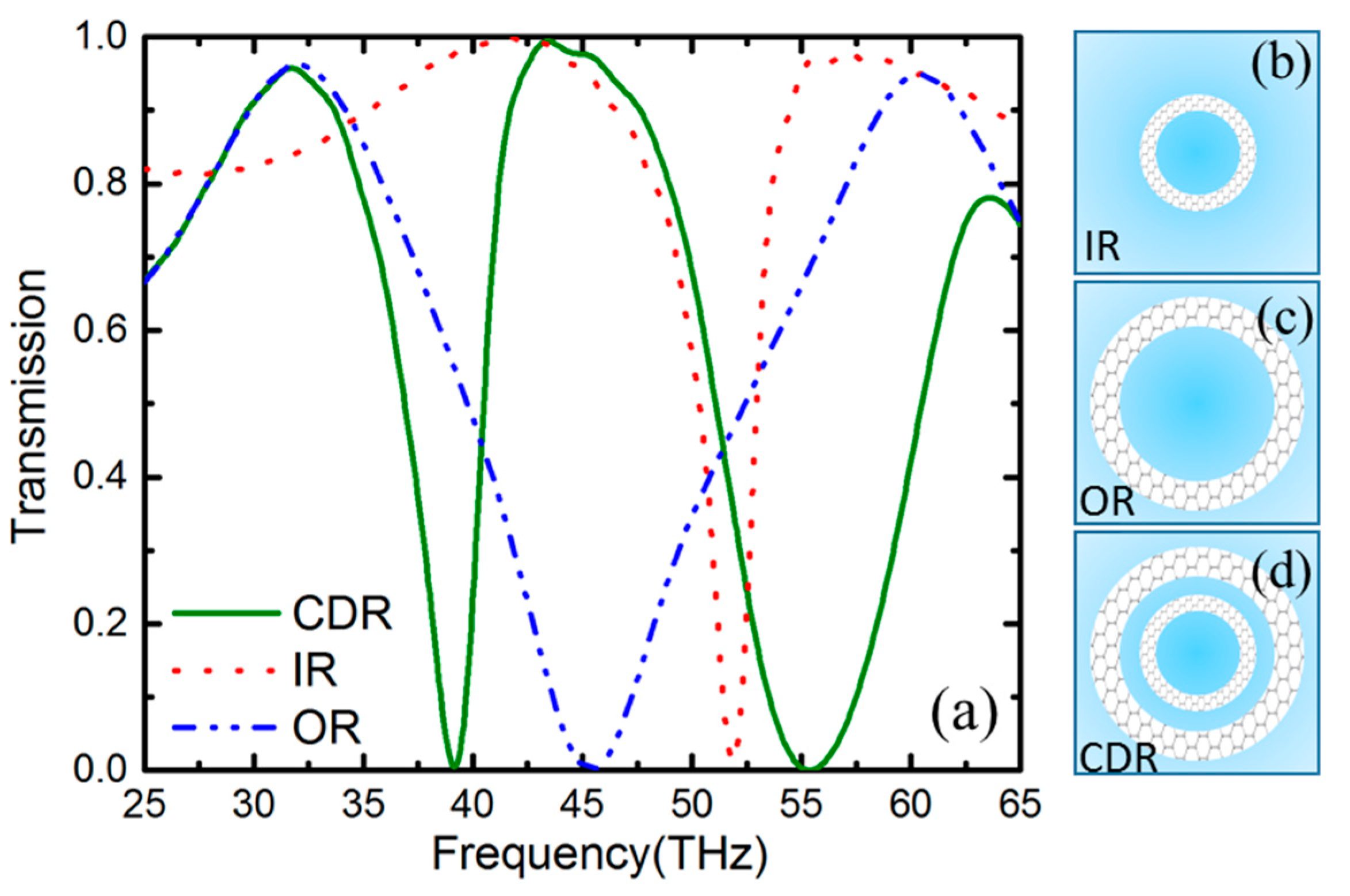
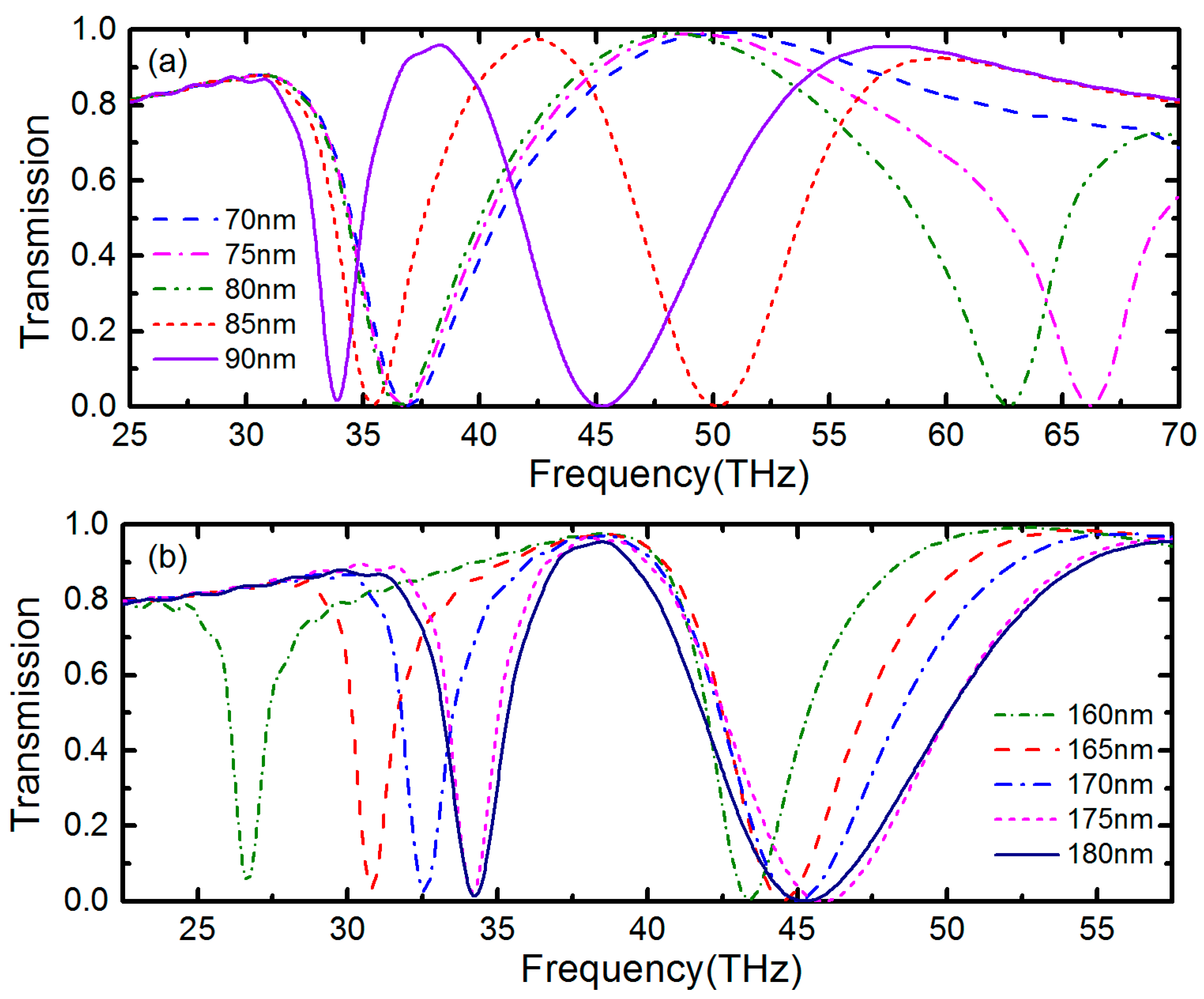
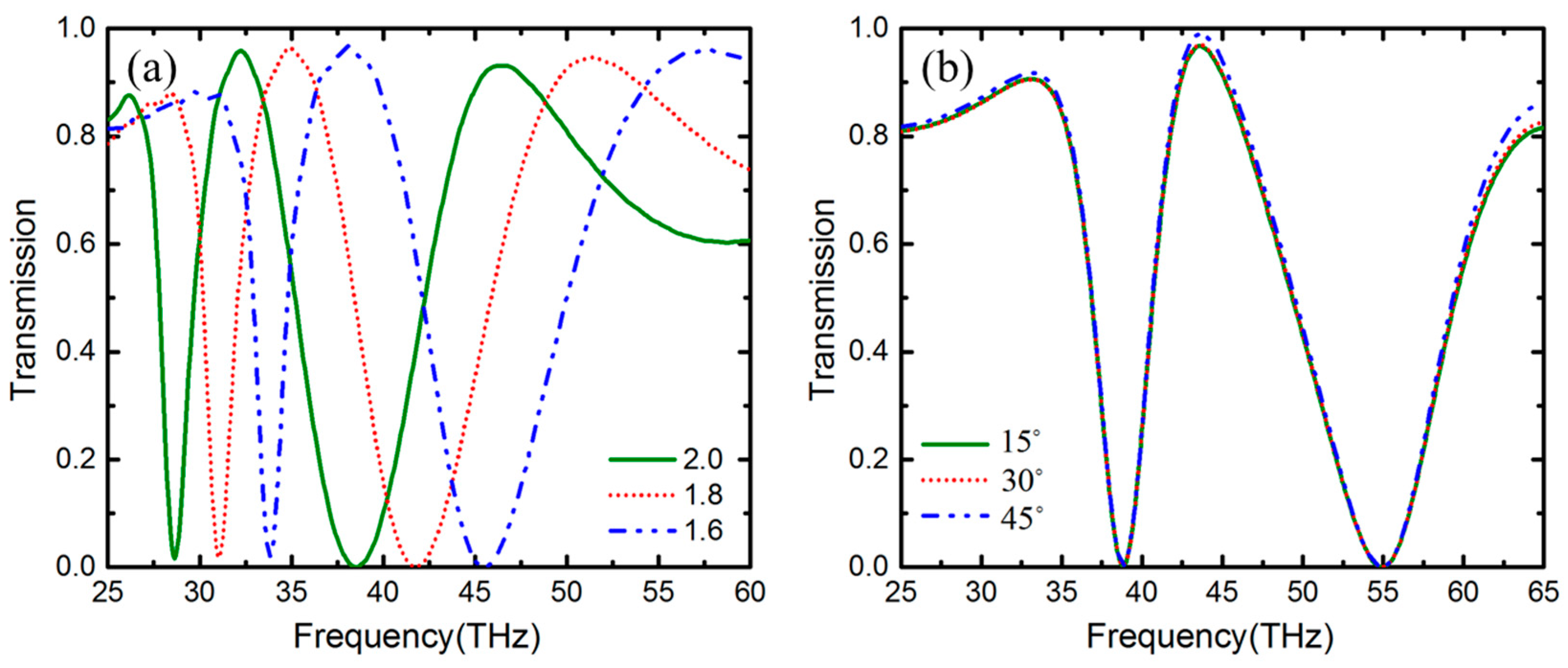
3. Results and Discussion

In order to demonstrate the PIT effect, we numerically calculated the transmission spectrum of the unit cell with different patterned graphene structures. As shown in Figure 3a, the red dot line, blue dash line, and olive solid line respectively represent the transmission spectrum of the unit cell corresponding to only IR (Figure 3b), only OR (Figure 3c) and CDR (Figure 3d) structures, and the other geometric parameters keep the same as in Figure 1. It is obvious that the plasmonic resonances of the IR and OR structure are excited at different frequencies, explained by the Fabry–Perot model. When the frequency is 51.9 THz, the transmission of the IR structure is close to 0, but for the OR structure, the lowest transmission appears at 45.4 THz. For the proposed CDR structure, there are two plasomonic resonance peaks at 39.1 and 55.4 THz observed, and a transparency window is found at the frequency of 44.1 THz. Particularly, the amplitude of transparency window is very high. There exists light transmission for CDR structure at the frequency band where there is no light transmission for OR structures. Therefore, the PIT phenomena could be produced in the unit cell of CDR structure by combining IR and OR. The reason why this PIT phenomenon appears is the interference between the bright and dark modes via near-field coupling, which could be explained by the plasmonic hybridization model (PHM) in theory [40].
To further clarify the mechanism of the transparent window, three sets of unit cells with different structures were investigated. The corresponding electric field distributions at plasomonic resonance peaks are shown in Figure 4, where the absorption is extremely strong. According to Figure 4a,b, we could find that the electric field is mainly distributed at the edge of the ring-shaped graphene. Besides, there exists electric field interaction in the gap between IR and OR, which we could obtain from Figure 4c,d. Therefore, the PIT phenomenon is produced by interference between the bright modes and the dark modes from IR and OR via near-field coupling based on the corresponding edge mode, which can be explained by PHM. The interference is closely related to the structure parameters of the unit cell and directly have an influence on the position of frequency and the full wave at half maximum (FWHM) of the transparency window. The width of gap wg between IR and OR is the main factor we would consider firstly. As shown in Figure 5, in this case the width of IR wi and OR wo remain unchanged, Figure 5a is the transmission spectrum when changing the radius of IR but keeping the radius of OR the same as Figure 1, and Figure 5b is the transmission spectrum when changing the radius of OR but keeping the radius of IR the same as Figure 1. When we change the outer radius of IR or the inner radius of OR to increase the width of the gap wg, there is a blueshift in the transmission. The FWHM of transparency window also changes with the width of the gap wg increasing. For instance, the FWHM is broadened from 7.9 to 13.2 THz when the width of the gap increases from 48 to 68 nm in Figure 5a.
Then, the relationships between transmission spectrum and width of IR and OR are also demonstrated. As depicted in Figure 6, we maintain the other geometrical parameters unchanged, including the width of the gap, and only change the inner radius (ri) of IR or outer radius (ro + wo) of OR. As the inner radius of IR decreases, the frequency of transmission window experiences a blue shift and the FWHM of it broadens, over 20 THz at the inner radius of 80 nm. The amplitude of transparency window also increases with the inner radius of IR decreasing. When the inner radius of IR is less than 75 nm, the PIT phenomenon disappears from transmission spectrum. When we change the outer radius of OR, the transparency window also could be adjusted, including frequency, FWHM and amplitude. Additionally, we could find that the width of OR mainly influences high frequency plasomonic resonance peak and the width of IR mainly influences low frequency plasomonic resonance peak.
The frequency tunability of PIT is a significant important feature in practical application. The imaginary part of the conductivity of graphene determines the spectral shift of the resonance, and the real part controls the amplitude modulation of the resonance [41]. Hence, the transparency window could be adjusted indirectly by tuning the Fermi level via the applied gate voltage or chemical doping. Figure 7a plots the transmission spectrum for different values of μc, 0.5, 0.6 and 0.7 eV, respectively. As the Fermi energy increases, the frequencies of the transparency window tend to exhibit a blueshift. However, the FWHM and amplitude of transparency window for different Fermi energy are approximately same. As shown in Figure 7b, slow light, as one of the most important applications of PIT, is also studied for different Fermi energy. The slow light could be qualified by the delay time τg [42]:
τ g = d ψ ( ω i l ) d ω i l ,
where ωil is the circular frequency of incident light, and ψ(ωil) is the transmission phase shift from the light source to calculated point. When the Fermi energy is at 0.7 eV, there is a slow light region due to the extreme dispersion within the transparency window. Additionally, the slow light region experiences a redshift with the Fermi energy decreasing. As a result, the frequency of transparency window and slow light could be electrically controlled.
Furthermore, we investigated the effect of refractive index of substrate on the transmission spectrum. In Figure 8a, we maintained the structure parameters unchanged and merely varied the refractive index of substrate from 1.6 to 2.0 successively. It is clear that the transmission spectrum exhibits a redshift with the increasing index. Additionally, the FWHM of the transparency window becomes narrower. In addition, the PIT phenomenon under oblique incidence is researched in Figure 8b. The incident angle is defined as the angle between the incident wave and negative z-direction, varying from 15° to 45°. It is obvious that the transmission spectrum is independent of the incident angle. Besides, due to the central symmetry of the structure, the transmission is insensitive to the polarization angle.

4. Conclusions

To conclude, we have proposed a monolayer-graphene-based CDR structure to realize broadband PIT on the strength of edge mode in the mid-infrared spectrum. The frequency and bandwidth of the transparency window could be effectively adjusted and controlled via changing the geometrical parameters of graphene or applying different gate voltages. The simulation results show that the structure has two plasomonic resonance peaks at 39.1 and 55.4 THz, and a transparency window with high amplitude at the frequency of 44.1 THz. The transmission spectra experience blue shift when the Fermi energy of graphene increases or refractive index of the substrate decreases. The bandwidth of the transparency window is broadened by increasing the width of the gap, IR or OR. Besides, the transmission is insensitive to polarization angle and incident angle. We believe that our research could be used in many future device applications, such as optical switches and slow light modulators in the mid-infrared region.

Author Contributions

H.X. did the simulation and wrote the paper. J.Y., J.O. and Z.Z. proposed the idea and revised the manuscript. S.W. and Y.L. gave some theorical advices. J.Z. and D.C. provided some simulation advices. J.Y. provided the research funding.

Funding

This research was funded by the Foundation of NUDT, grant number JC13-02-13, ZK17-03-01, the Hunan Provincial Natural Science Foundation of China, grant number 13JJ3001, and the Program for New Century Excellent Talents in University, grant number NCET-12-0142.

Conflicts of Interest

The authors declare no conflict of interest.

References

  1. Novoselov, K.S.; Geim, A.K.; Morozov, S.V.; Jiang, D.; Zhang, Y.; Dubonos, S.V. Electric field effect in atomically thin carbon films. Science 2004, 306, 666–669. [Google Scholar] [CrossRef] [PubMed]
  2. Deng, G.; Chen, P.; Yang, J.; Yin, Z.; Qiu, L. Graphene-based tunable polarization sensitive terahertz metamaterial absorber. Opt. Commun. 2016, 380, 101–107. [Google Scholar] [CrossRef]
  3. Fan, Y.; Guo, C.; Zhu, Z.; Xu, W.; Wu, F.; Yuan, X.; Qin, S. Monolayer-graphene-based broadband and wide-angle perfect absorption structures in the near infrared. Sci. Rep. 2018, 8, 13709–13715. [Google Scholar] [CrossRef] [PubMed]
  4. Wang, D.; Liu, X.; He, L.; Lin, Y.; Wu, D.; Shi, J. Manipulating graphene mobility and charge neutral point with ligand-bound nanoparticles as charge reservoir. Nano Lett. 2010, 10, 4989–4993. [Google Scholar] [CrossRef] [PubMed]
  5. Garcia de Abajo, F.J. Graphene Plasmonics: Challenges and Opportunities. ACS Photonics 2014, 1, 135–152. [Google Scholar] [CrossRef] [Green Version]
  6. Xu, B.; Gu, C.; Li, Z.; Liu, L.; Niu, Z. A Novel Absorber with Tunable Bandwidth Based on Graphene. IEEE Antennas Wirel. Propag. Lett. 2014, 13, 822–825. [Google Scholar]
  7. Xiong, F.; Zhang, J.; Zhu, Z.; Yuan, X.; Qin, S. Ultrabroadband, More than One Order Absorption Enhancement in Graphene with Plasmonic Light Trapping. Sci. Rep. 2015, 5, 16998. [Google Scholar] [CrossRef] [Green Version]
  8. He, X.; Zhong, X.; Lin, F.; Shi, W. Investigation of graphene assisted tunable terahertz metamaterials absorber. Opt. Mater. Express 2016, 6, 331–342. [Google Scholar] [CrossRef]
  9. Hanson, G.W. Dyadic Green’s functions and guided surface waves for a surface conductivity model of graphene. J. Appl. Phys. 2008, 103, 19912–19918. [Google Scholar] [CrossRef]
  10. Yee, K.J.; Kim, J.H.; Jung, M.H.; Hong, B.H.; Kong, K.J. Ultrafast modulation of optical transitions in monolayer and multilayer graphene. Carbon 2011, 49, 4781–4785. [Google Scholar] [CrossRef]
  11. Meng, H.; Wang, L.; Liu, G.; Xue, X.; Lin, Q.; Zhai, X. Tunable graphene-based plasmonic multispectral and narrowband perfect metamaterial absorbers at the mid-infrared region. Appl. Opt. 2017, 56, 6022–6027. [Google Scholar] [CrossRef] [PubMed]
  12. Bonaccorso, F.; Sun, Z.; Hasan, T.; Ferrari, A. Graphene photonics and optoelectronics. Nat. Photonics 2010, 4, 611–622. [Google Scholar] [CrossRef] [Green Version]
  13. Bao, Q.; Loh, K.P. Graphene photonics, plasmonics, and broadband optoelectronic devices. ACS Nano 2012, 6, 3677–3694. [Google Scholar] [CrossRef] [PubMed]
  14. Xia, F.; Wang, H.; Xiao, D.; Dubey, M.A. Ramasubramaniam, Two-dimensional material nanophotonics. Nat. Photonics 2014, 8, 899–907. [Google Scholar] [CrossRef]
  15. Wang, X.; Zhi, L.; Müllen, K. Transparent conductive graphene electrodes for dye-sensitized solar cells. Nano Lett. 2008, 8, 323–327. [Google Scholar] [CrossRef]
  16. Ma, Q.; Zhan, Y.; Hong, W. Tunable Metamaterial with Gold and Graphene Split-Ring Resonators and Plasmonically Induced Transparency. Nanomaterials 2018, 9, 7. [Google Scholar] [CrossRef] [PubMed]
  17. Liu, C.; Zha, S.; Liu, P.; Yang, C.; Zhou, Q. Electrical Manipulation of electromagnetically induced transparency for slow light purpose based on metal-graphene hybrid metamaterial. Appl. Sci. 2018, 8, 2672. [Google Scholar] [CrossRef]
  18. Chen, J.; Wang, C.; Zhang, R.; Xiao, J. Multiple plasmon-induced transparencies in coupled-resonator systems. Opt. Lett. 2012, 37, 5133–5135. [Google Scholar] [CrossRef]
  19. Halas, N.J.; Lal, S.; Chang, W.S.; Link, S.; Nordlander, P. Plasmons in strongly coupled metallic nanostructures. Chem. Rev. 2011, 111, 3913–3961. [Google Scholar] [CrossRef]
  20. Shahamat, Y.; Vahedi, M. Plasmon-induced transparency in a rectangle cavity and an H-shaped structure for sensing and switching applications. J. Nanophotonics 2017, 11, 046012. [Google Scholar] [CrossRef]
  21. Tang, C.; Niu, Q.; Wang, B.X.; Huang, W.Q. Design of Dual-Band Plasmon-Induced Transparent Effect Based on Composite Structure of Closed-Ring and Square Patch. Plasmonics 2018, 2018, 1–6. [Google Scholar] [CrossRef]
  22. Nong, J.; Wei, W.; Wang, W.; Lan, G.; Shang, Z.; Yi, J.; Tang, L. Strong coherent coupling between graphene surface plasmons and anisotropic black phosphorus localized surface plasmons. Opt. Express 2018, 26, 1633–1644. [Google Scholar] [CrossRef] [PubMed]
  23. Habib, M.; Rashed, A.R.; Ozbay, E.; Caglayan, H. Graphene-based tunable plasmon induced transparency in gold strips. Opt. Mater. Express 2018, 8, 1069–1074. [Google Scholar] [CrossRef]
  24. Verellen, N.; Sonnefraud, Y.; Sobhani, H.; Hao, F.; Moshchalkov, V.V.; Van Dorpe, P.; Nordlander, P.; Maier, S.A. Fano resonances in individual coherent plasmonic nanocavities. Nano Lett. 2009, 9, 1663–1667. [Google Scholar] [CrossRef] [PubMed]
  25. Cheng, H.; Chen, S.; Yu, P.; Duan, X.; Xie, B.; Tian, J. Dynamically tunable plasmonically induced transparency in periodically patterned graphene nanostrips. Appl. Phys. Lett. 2013, 103, 203112. [Google Scholar] [CrossRef]
  26. Zare, M.S.; Nozhat, N.; Rashiditabar, R. Tunable graphene based plasmonic absorber with grooved metal film in near infrared region. Opt. Commun. 2017, 398, 56–61. [Google Scholar] [CrossRef]
  27. Zhang, H.; Cao, Y.; Liu, Y.; Li, Y.; Zhang, Y. Electromagnetically induced transparency based on cascaded π-shaped graphene nanostructure. Plasmonics 2017, 12, 1833–1839. [Google Scholar] [CrossRef]
  28. Tan, T.C.; Srivastava, Y.K.; Manjappa, M.; Plum, E.; Singh, R. Lattice induced strong coupling and line narrowing of split resonances in metamaterials. Appl. Phys. Lett. 2018, 112, 201111. [Google Scholar] [CrossRef] [Green Version]
  29. Zhou, F.; Zhang, L.; Wan, M.; Song, Y. Broadband plasmon-induced transparency in terahertz metamaterials via constructive interference of electric and magnetic couplings. Opt. Mater. Express 2015, 23, 27361–27368. [Google Scholar]
  30. Zhu, Z.; Yang, X.; Gu, J. Broadband plasmon induced transparency in terahertz metamaterials. Nanotechnology 2013, 24, 214003. [Google Scholar] [CrossRef]
  31. Jin, X.R.; Lu, Y.; Zheng, H.; Lee, Y.; Rhee, J.Y.; Kim, K.W.; Jang, W.H. Plasmonic electromagnetically induced transparency in metamaterial based on second-order plasmonic resonance. Opt. Commun. 2011, 284, 4766–4768. [Google Scholar] [CrossRef]
  32. Bai, Q.; Liu, C.; Chen, J.; Cheng, C.; Kang, M.; Wang, H.T. Tunable slow light in semiconductor metamaterial in a broad terahertz regime. J. Appl. Phys. 2010, 107, 093104. [Google Scholar]
  33. Li, C.; Qi, D.; Wang, Y.; Zhang, X. Wideband slow light based on plasmon-induced transparency at telecom frequency. Opt. Commun. 2015, 51, 26–29. [Google Scholar] [CrossRef]
  34. Zhang, Z.; Yang, J.; He, X.; Han, Y.; Zhang, J.; Huang, J.; Chen, D. Active control of broadband plasmon induced transparency in a terahertz hybrid metal graphene metamaterial. RSC Adv. 2018, 8, 27746–27753. [Google Scholar] [CrossRef]
  35. Han, L.; Wang, L.; Xing, H.; Chen, X. Anisotropic plasmon induced transparency in black phosphorus nanostrip trimer. Opt. Mater. Express 2019, 9, 352–361. [Google Scholar] [CrossRef]
  36. Jiang, L.; Tang, J.; Xu, J.; Zheng, Z.; Dong, J.; Guo, J.; Qian, S.; Dai, X.; Xiang, Y. Graphene Tamm plasmon-induced low-threshold optical bistability at terahertz frequencies. Opt. Mater. Express 2018, 9, 139–150. [Google Scholar] [CrossRef]
  37. Cao, W.; Singh, R.; Zhang, C.; Han, J.; Tonouchi, M.W. Zhang, Plasmon-induced transparency in metamaterials: Active near field coupling between bright superconducting and dark metallic mode resonators. Appl. Phys. Lett. 2013, 103, 101106. [Google Scholar] [CrossRef]
  38. Biabanifard, S.; Biabanifard, M.; Asgari, S.; Asadi, S.; Vagoub, M.C.E. Tunable ultra-wideband terahertz absorber based on graphene disks and ribbons. Opt. Commun. 2018, 427, 418–425. [Google Scholar] [CrossRef]
  39. Taflove, A.; Hagness, S.C. Computational Electrodynamics, The Finite-Difference Time-Domain Method, 3rd ed.; Artech House: Boston, FL, USA, 2005; pp. 107–112. [Google Scholar]
  40. Xiao, S.; Wang, T.; Liu, T.; Yan, X.; Li, Z.; Xu, C. Active modulation of electromagnetically induced transparency analogue in terahertz hybrid metal-graphene metamaterials. Carbon 2018, 126, 271–278. [Google Scholar] [CrossRef] [Green Version]
  41. Cai, Y.; Zhu, J.Q.; Liu, H. Tunable enhanced optical absorption of graphene using plasmonic perfect absorbers. Appl. Phys. Lett. 2015, 106, 043105. [Google Scholar] [CrossRef]
  42. Prodan, E.; Radloff, C.; Halas, N.J.; Nordlander, P. A Hybridization Model for the Plasmon Response of Complex Nanostructures. Science 2003, 302, 419–422. [Google Scholar] [CrossRef] [PubMed]
Figure 1. Schematic of the geometry of the proposed monolayer graphene-based concentric-double-rings (CDR) structure. (a) The top view of the unit cell: the periodic graphene nanostructure arrays with radius of inner-ring ri = 90 nm, width wi = 10 nm, radius of outer-ring ro = 148 nm, width wo = 30 nm, and period px = 400 nm and py = 400 nm. (b) The side view of the unit cell: the thickness of graphene tg = 1 nm, the thickness of dielectric td = 2 μm.
Nanomaterials 09 00448 g001
Figure 2. Diagram of graphene conductivity (a) real part (b) imaginary part at different Fermi levels.
Nanomaterials 09 00448 g002
Figure 3. (a) Transmission spectrum corresponding to the unit cell with an inner ring (IR), an outer ring (OR) and a concentric-double-ring (CDR). The Fermi energy of graphene is fixed at 0.64 eV and the refractive index of dielectric is set as 1.6 in the simulations. (bd) Structural representation of IR, OR and CDR, respectively.
Nanomaterials 09 00448 g003
Figure 4. The electric field distributions at (a) 51.9 THz when the structure of graphene is individual IR, (b) 45.4 THz when the structure of graphene is individual OR. The electric field distributions at (c) 55.4 THz, (d) 39.1 THz when the structure of graphene is CDR.
Nanomaterials 09 00448 g004
Figure 5. Transmission spectrum corresponding to different widths of the gap, 38, 48, 58 and 68 nm, respectively. (a) Keeping the geometric parameters of OR same and changing the radius of IR. (b) Keeping the geometric parameters of IR same and changing the radius of OR.
Nanomaterials 09 00448 g005
Figure 6. Transmission spectrum for (a) different inner radii of IR and (b) different outer radii of OR with other geometrical parameters unchanged.
Nanomaterials 09 00448 g006
Figure 7. (a) Transparency spectrum for different Fermi energy of graphene from 0.5 to 0.7 eV. (b) Slow light region corresponding to different Fermi energy of graphene.
Nanomaterials 09 00448 g007
Figure 8. Transmission spectrum corresponding to (a) different refractive indexes (b) different incident angles.
Nanomaterials 09 00448 g008

