Multi-Level Cell Properties of a Bilayer Cu2O/Al2O3 Resistive Switching Device


Abstract
1. Introduction
2. Materials and Methods
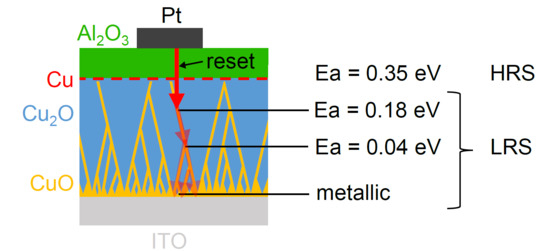
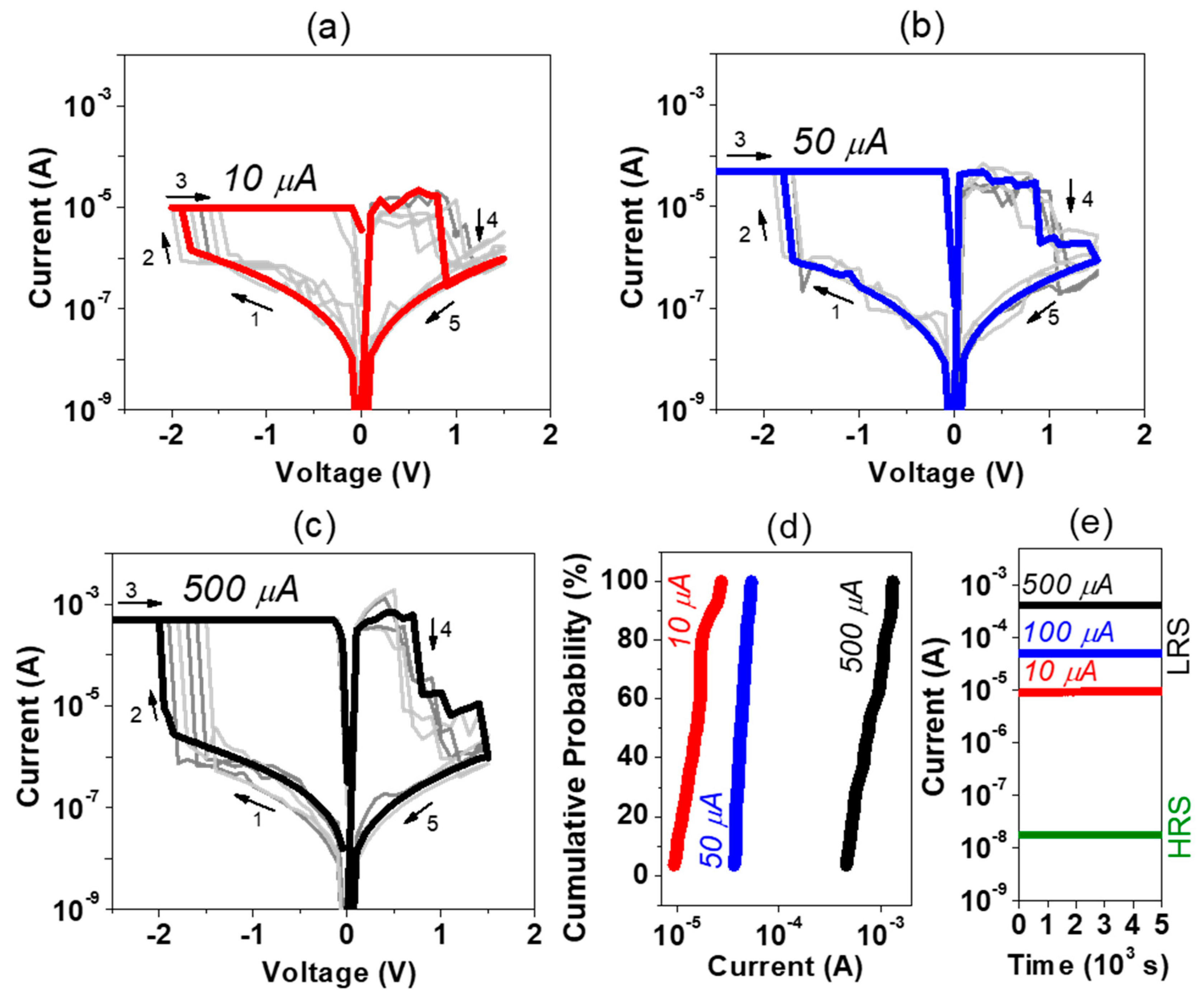
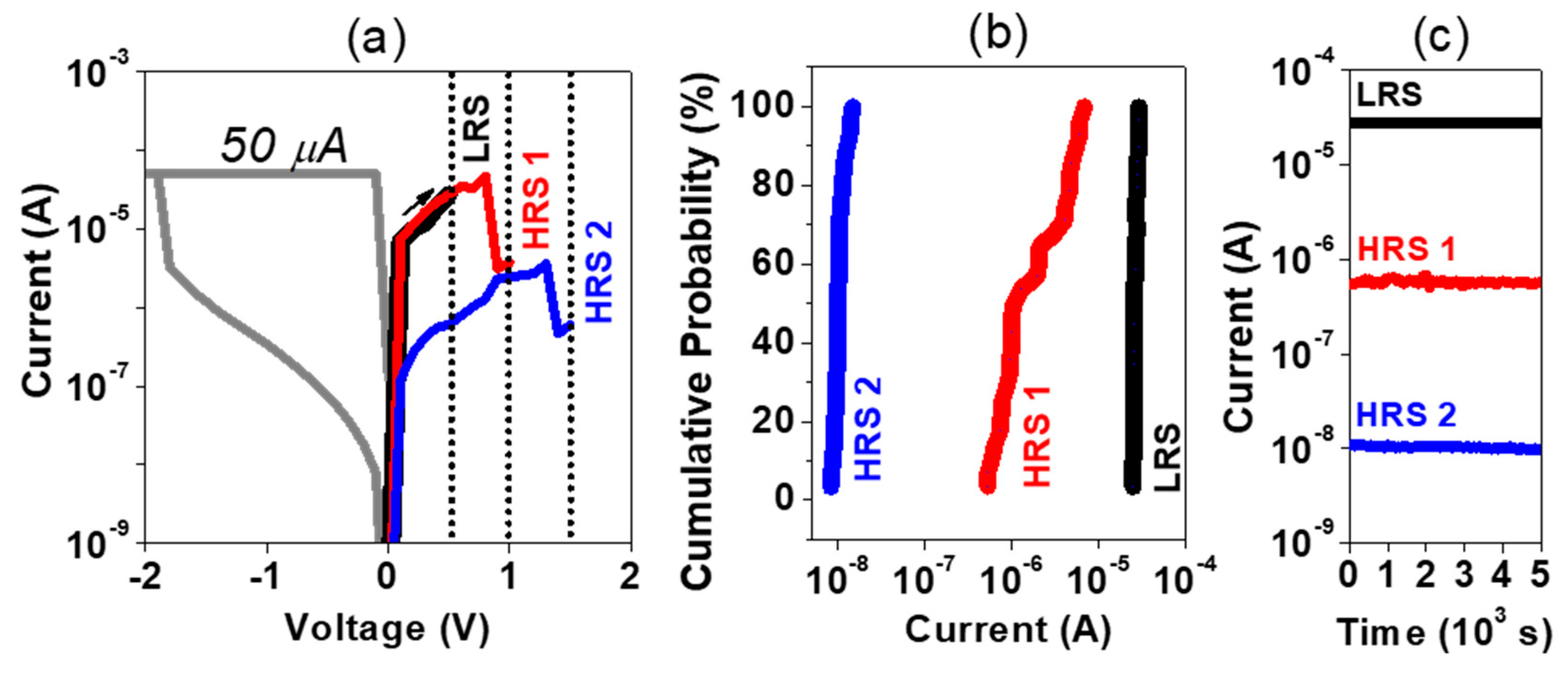
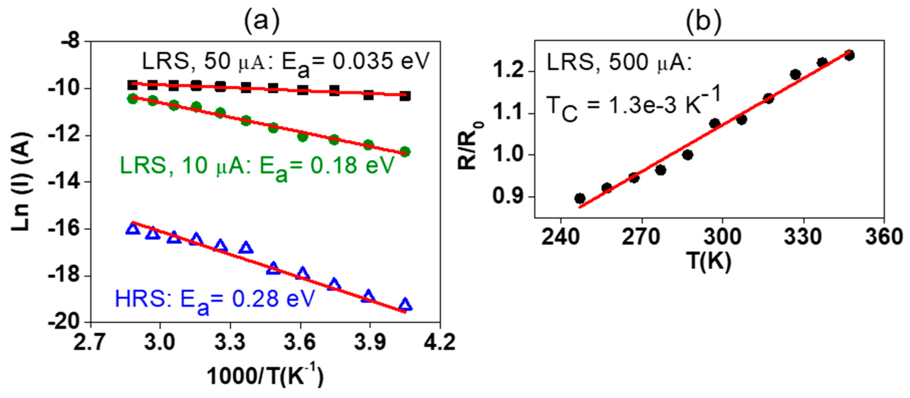
3. Results
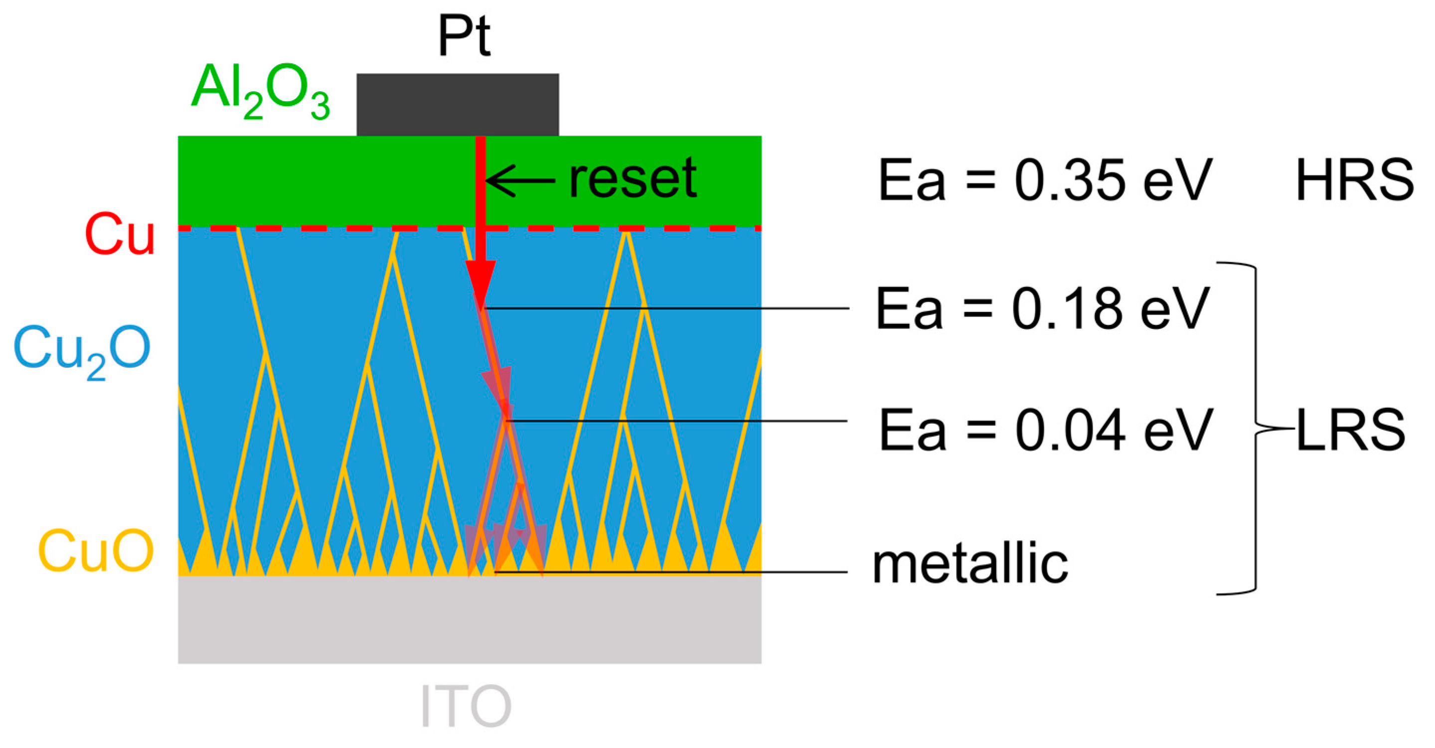
4. Discussion
5. Conclusions
Author Contributions
Funding
Conflicts of Interest
References
- Yang, J.J.; Pickett, M.D.; Li, X.; Ohlberg, D.A.A.; Stewart, D.R.; Williams, R.S. Memristive switching mechanism for metal/oxide/metal nanodevices. Nat. Nanotechnol. 2008, 3, 429–433. [Google Scholar] [CrossRef] [PubMed]
- Jana, D.; Roy, S.; Panja, R.; Dutta, M.; Rahaman, S.Z.; Mahapatra, R.; Maikap, S. Conductive-bridging random access memory: Challenges and opportunity for 3D architecture. Nanoscale Res. Lett. 2015, 10, 188. [Google Scholar] [CrossRef] [PubMed]
- Pei, Y.; Mai, B.; Zhang, X.; Hu, R.; Li, Y.; Chen, Z.; Fan, B.; Liang, J.; Wang, G. Performance improvement of amorphous indium-gallium-zinc oxide ReRAM with SiO2 inserting layer. Curr. Appl. Phys. 2015, 15, 441–445. [Google Scholar] [CrossRef]
- Robertson, J. High dielectric constant oxides. Eur. Phys. J. Appl. Phys. 2004, 28, 265–291. [Google Scholar] [CrossRef]
- Carlos, E.; Branquinho, R.; Kiazadeh, A.; Barquinha, P.; Martins, R.; Fortunato, E. UV-Mediated Photochemical Treatment for Low-Temperature Oxide-Based Thin-Film Transistors. ACS Appl. Mater. Interfaces 2016, 8, 31100–31108. [Google Scholar] [CrossRef] [PubMed]
- Cook, E.L. Model for the resistive-conductive transition in reversible resistance-switching solids. J. Appl. Phys. 1970, 41, 551–554. [Google Scholar] [CrossRef]
- Zarabi, M.J.; Satyam, M. Switching in copper oxide. J. Appl. Phys. 1974, 45, 775–780. [Google Scholar] [CrossRef]
- Wang, G.J.; Weichman, F.L. The temperature dependence of the electrical conductivity and switching phenomena in Cu2O single crystals. Can. J. Phys. 1982, 60, 1648–1655. [Google Scholar] [CrossRef]
- Yang, W.Y.; Rhee, S.W. Effect of electrode material on the resistance switching of Cu2O film. Appl. Phys. Lett. 2007, 91, 232907. [Google Scholar] [CrossRef]
- Yan, P.; Li, Y.; Hui, Y.J.; Zhong, S.J.; Zhou, Y.X.; Xu, L.; Liu, N.; Qian, H.; Sun, H.J.; Miao, X.S. Conducting mechanisms of forming-free TiW/Cu2O/Cu memristive devices. Appl. Phys. Lett. 2015, 107, 083501. [Google Scholar] [CrossRef]
- Singh, B.; Mehta, B.R.; Varandani, D.; Savu, A.V.; Brugger, J. CAFM investigations of filamentary conduction in Cu2O ReRAM devices fabricated using stencil lithography technique. Nanotechnology 2012, 23, 495707. [Google Scholar] [CrossRef] [PubMed]
- Deuermeier, J.; Liu, H.; Rapenne, L.; Calmeiro, T.; Renou, G.; Martins, R.; Muñoz-Rojas, D.; Fortunato, E. Visualization of nanocrystalline CuO in the grain boundaries of Cu2O thin films and effect on band bending and film resistivity. APL Mater. 2018, 6, 096103. [Google Scholar] [CrossRef]
- Deuermeier, J.; Wardenga, H.F.; Morasch, J.; Siol, S.; Nandy, S.; Calmeiro, T.; Klein, A.; Fortunato, E. Highly conductive grain boundaries in copper oxide thin films. J. Appl. Phys. 2016, 119, 235303. [Google Scholar] [CrossRef]
- Bersuker, G.; Yum, J.; Iglesias, V.; Porti, M.; Nafría, M.; Mckenna, K.; Shluger, A.; Kirsch, P.; Jammy, R. Grain boundary-driven leakage path formation in HfO2 dielectrics. In Proceedings of the 40th European Solid State Device Research Conference, Sevilla, Spain, 14–16 September 2010; pp. 333–336. [Google Scholar]
- Lanza, M. A review on resistive switching in high-k dielectrics: A nanoscale point of view using conductive atomic force microscope. Materials 2014, 7, 2155–2182. [Google Scholar] [CrossRef] [PubMed]
- Valov, I.; Waser, R.; Jameson, J.R.; Kozicki, M.N. Electrochemical metallization memories—fundamentals, applications, prospects. Nanotechnology 2011, 22, 254003. [Google Scholar] [CrossRef] [PubMed]
- Hubbard, W.A.; Kerelsky, A.; Jasmin, G.; White, E.R.; Lodico, J.; Mecklenburg, M.; Regan, B.C. Nanofilament Formation and Regeneration during Cu/Al2O3 Resistive Memory Switching. Nano Lett. 2015, 15, 3983–3987. [Google Scholar] [CrossRef] [PubMed]
- Celano, U.; Goux, L.; Belmonte, A.; Opsomer, K.; Franquet, A.; Schulze, A.; Detavernier, C.; Richard, O.; Bender, H.; Jurczak, M.; et al. Three-dimensional observation of the conductive filament in nanoscaled resistive memory devices. Nano Lett. 2014, 14, 2401–2406. [Google Scholar] [CrossRef]
- Yang, Y.; Gao, P.; Li, L.; Pan, X.; Tappertzhofen, S.; Choi, S.; Waser, R.; Valov, I.; Lu, W.D. Electrochemical dynamics of nanoscale metallic inclusions in dielectrics. Nat. Commun. 2014, 5, 1–9. [Google Scholar] [CrossRef]
- Tappertzhofen, S.; Hofmann, S. Embedded nanoparticle dynamics and their influence on switching behaviour of resistive memory devices. Nanoscale 2017, 9, 17494–17504. [Google Scholar] [CrossRef]
- Liu, M.; Abid, Z.; Wang, W.; He, X.; Liu, Q.; Guan, W. Multilevel resistive switching with ionic and metallic filaments. Appl. Phys. Lett. 2009, 94, 233106. [Google Scholar] [CrossRef]
- Zhang, Y.; Wu, H.; Bai, Y.; Chen, A.; Yu, Z.; Zhang, J.; Qian, H.; Zhang, Y.; Wu, H.; Bai, Y.; et al. Study of conduction and switching mechanisms in Al/AlOx/WOx/W resistive switching memory for multilevel applications. Appl. Phys. Lett. 2013, 102, 233502. [Google Scholar] [CrossRef]
- Belmonte, A.; Kim, W.; Chan, B.T.; Heylen, N.; Fantini, A.; Houssa, M.; Jurczak, M.; Goux, L. A thermally stable and high-performance 90-nm Al2O3/Cu-based 1T1R CBRAM cell. IEEE Trans. Electron. Devices 2013, 60, 3690–3695. [Google Scholar] [CrossRef]
- Goux, L.; Opsomer, K.; Degraeve, R.; Müller, R.; Detavernier, C.; Wouters, D.J.; Jurczak, M.; Altimime, L.; Kittl, J.A. Influence of the Cu-Te composition and microstructure on the resistive switching of Cu-Te/Al2O3/Si cells. Appl. Phys. Lett. 2011, 99, 053502. [Google Scholar] [CrossRef]
- Lim, S.; Lee, S.; Woo, J.; Lee, D.; Prakash, A.; Hwang, H. Effects of N-Doped GeSbTe Buffer Layer on Switching Characteristics of Cu/Al2O3-Based CBRAM. ECS Solid State Lett. 2015, 4, Q25–Q28. [Google Scholar] [CrossRef]
- Deuermeier, J.; Bayer, T.J.M.; Yanagi, H.; Kiazadeh, A.; Martins, R.; Klein, A.; Fortunato, E. Substrate reactivity as the origin of Fermi level pinning at the Cu2O/ALD-Al2O3 interface. Mater. Res. Express 2016, 3, 046404. [Google Scholar] [CrossRef]
- Rocha, P.R.F.; Kiazadeh, A.; De Leeuw, D.M.; Meskers, S.C.J.; Verbakel, F.; Taylor, D.M.; Gomes, H.L. The role of internal structure in the anomalous switching dynamics of metal-oxide/polymer resistive random access memories. J. Appl. Phys. 2013, 113, 134504. [Google Scholar] [CrossRef]
- Wu, E.Y.; Aitken, J.; Nowak, E.; Vayshenker, A.; Varekamp, P.; Hueckel, G.; McKenna, J.; Harmon, D.; Han, L.-K.; Montrose, C.; et al. Voltage-dependent voltage-acceleration of oxide breakdown for ultra-thin oxides. In Proceedings of the 30th International Electron Devices Meeting, San Francisco, CA, USA, 10–13 December 2000; pp. 541–544. [Google Scholar]
- Valov, I.; Tsuruoka, T. Effects of moisture and redox reactions in VCM and ECM resistive switching memories. J. Phys. D Appl. Phys. 2018, 51, 413001. [Google Scholar] [CrossRef]
- Grzesik, Z.; Migdalska, M.; Mrowec, S. Chemical diffusion in non-stoichiometric cuprous oxide. J. Phys. Chem. Solids 2008, 69, 928–933. [Google Scholar] [CrossRef]
- Porat, O.; Riess, I. Defect chemistry of Cu2-yO at elevated-temperatures. Part II: Electrical Conductivity, Thermoelectric Power and Charged Point Defects. Solid State Ionics 1995, 81, 29–41. [Google Scholar] [CrossRef]
- Brattain, W.H. The Copper Oxide Rectifier. Rev. Mod. Phys. 1951, 23, 203–212. [Google Scholar] [CrossRef]
- Meyer, B.K.; Polity, A.; Reppin, D.; Becker, M.; Hering, P.; Klar, P.J.; Sander, T.; Reindl, C.; Benz, J.; Eickhoff, M.; et al. Binary copper oxide semiconductors: From materials towards devices. Phys. Status Solidi B 2012, 249, 1487–1509. [Google Scholar] [CrossRef]
- Morasch, J.; Wardenga, H.F.; Jaegermann, W.; Klein, A. Influence of grain boundaries and interfaces on the electronic structure of polycrystalline CuO thin films. Phys. Status Solidi 2016, 213, 1615–1624. [Google Scholar] [CrossRef]
- Huang, Q.; Lilley, C.M.; Bode, M.; Divan, R.S. Electrical Properties of Cu Nanowires. In Proceedings of the 8th International Conference on Nanotechnology, Arlington, TX, USA, 18–21 August 2008; pp. 549–552. [Google Scholar]
- Cappella, A.; Battaglia, J.-L.; Schick, V.; Kusiak, A.; Lamperti, A.; Wiemer, C.; Hay, B. High Temperature Thermal Conductivity of Amorphous Al2O3 Thin Films Grown by Low Temperature ALD. Adv. Eng. Mater. 2013, 15, 1046–1050. [Google Scholar] [CrossRef]
- Timm, H.; Janek, J. On the Soret effect in binary nonstoichiometric oxides-kinetic demixing of cuprite in a temperature gradient. Solid State Ionics 2005, 176, 1131–1143. [Google Scholar] [CrossRef]
- Kumar, D.; Aluguri, R.; Chand, U.; Tseng, T.-Y. Enhancement of resistive switching properties in nitride based CBRAM device by inserting an Al2O3 thin layer. Appl. Phys. Lett. 2017, 110, 203102. [Google Scholar] [CrossRef]


© 2019 by the authors. Licensee MDPI, Basel, Switzerland. This article is an open access article distributed under the terms and conditions of the Creative Commons Attribution (CC BY) license (http://creativecommons.org/licenses/by/4.0/).
Share and Cite
Deuermeier, J.; Kiazadeh, A.; Klein, A.; Martins, R.; Fortunato, E. Multi-Level Cell Properties of a Bilayer Cu2O/Al2O3 Resistive Switching Device. Nanomaterials 2019, 9, 289. https://doi.org/10.3390/nano9020289
Deuermeier J, Kiazadeh A, Klein A, Martins R, Fortunato E. Multi-Level Cell Properties of a Bilayer Cu2O/Al2O3 Resistive Switching Device. Nanomaterials. 2019; 9(2):289. https://doi.org/10.3390/nano9020289
Chicago/Turabian StyleDeuermeier, Jonas, Asal Kiazadeh, Andreas Klein, Rodrigo Martins, and Elvira Fortunato. 2019. "Multi-Level Cell Properties of a Bilayer Cu2O/Al2O3 Resistive Switching Device" Nanomaterials 9, no. 2: 289. https://doi.org/10.3390/nano9020289
APA StyleDeuermeier, J., Kiazadeh, A., Klein, A., Martins, R., & Fortunato, E. (2019). Multi-Level Cell Properties of a Bilayer Cu2O/Al2O3 Resistive Switching Device. Nanomaterials, 9(2), 289. https://doi.org/10.3390/nano9020289