Soldering of Passive Components Using Sn Nanoparticle Reinforced Solder Paste: Influence on Microstructure and Joint Strength

 ,
,  ,
,
Abstract
1. Introduction
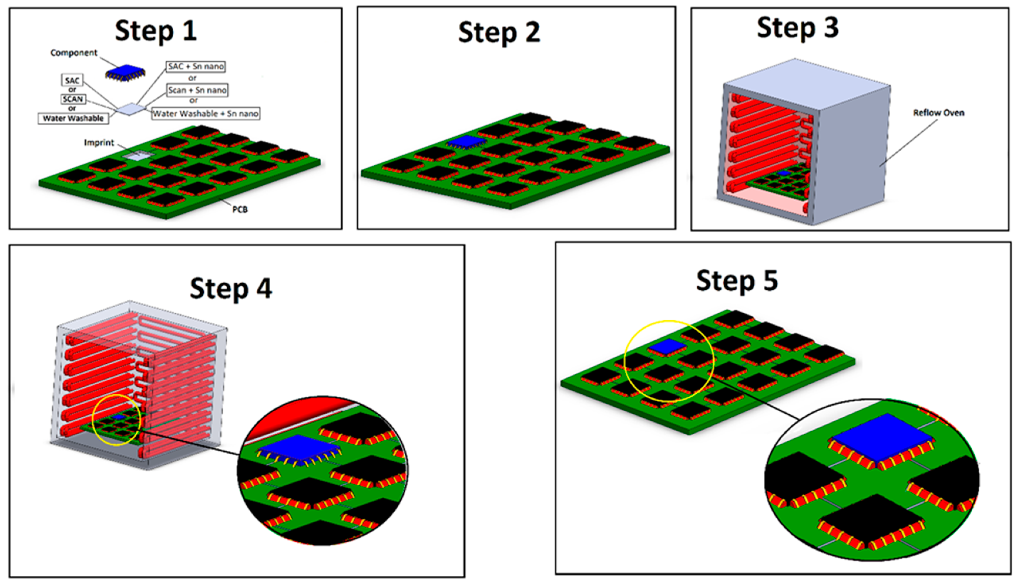
2. Methodology
3. Results and Discussion
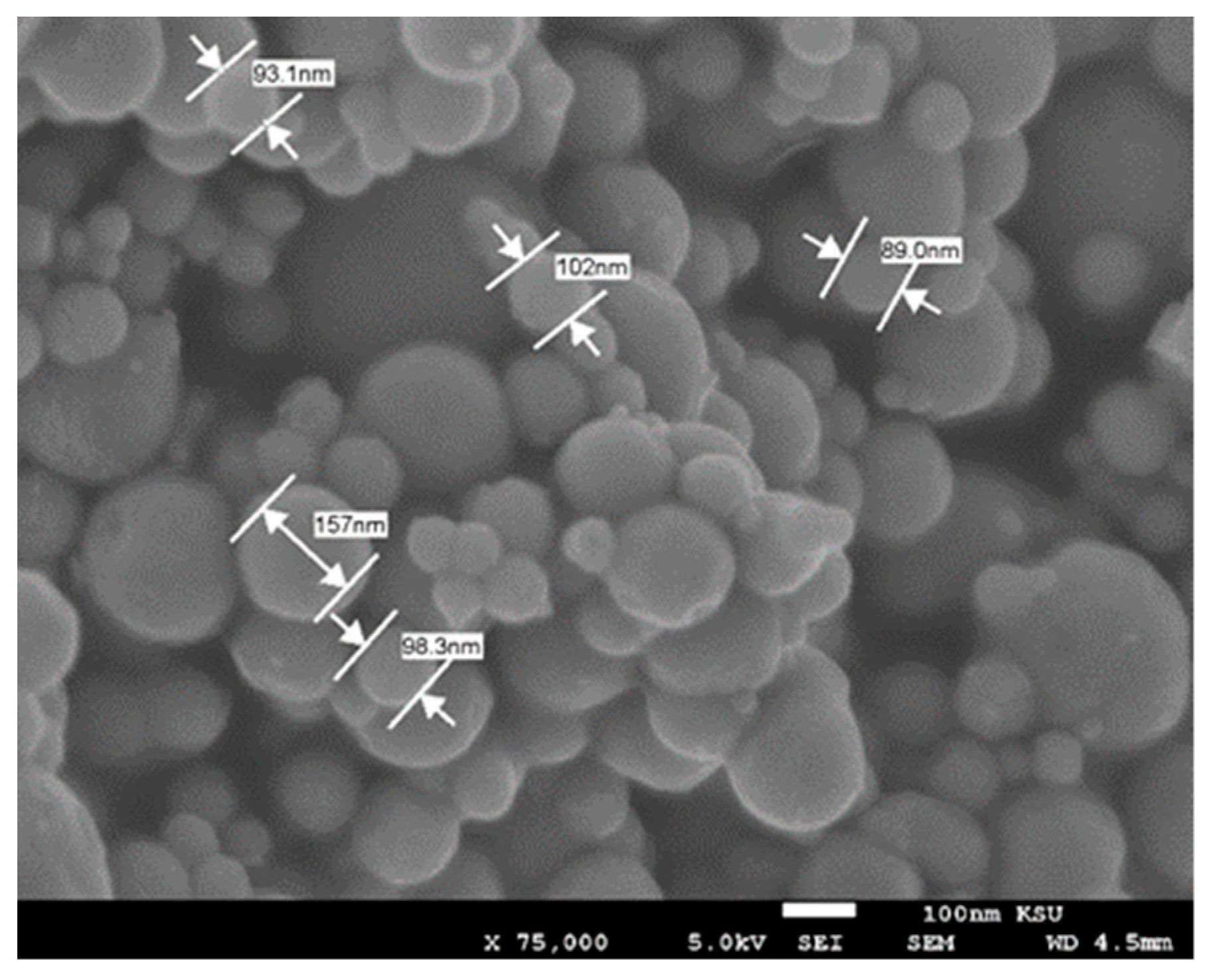
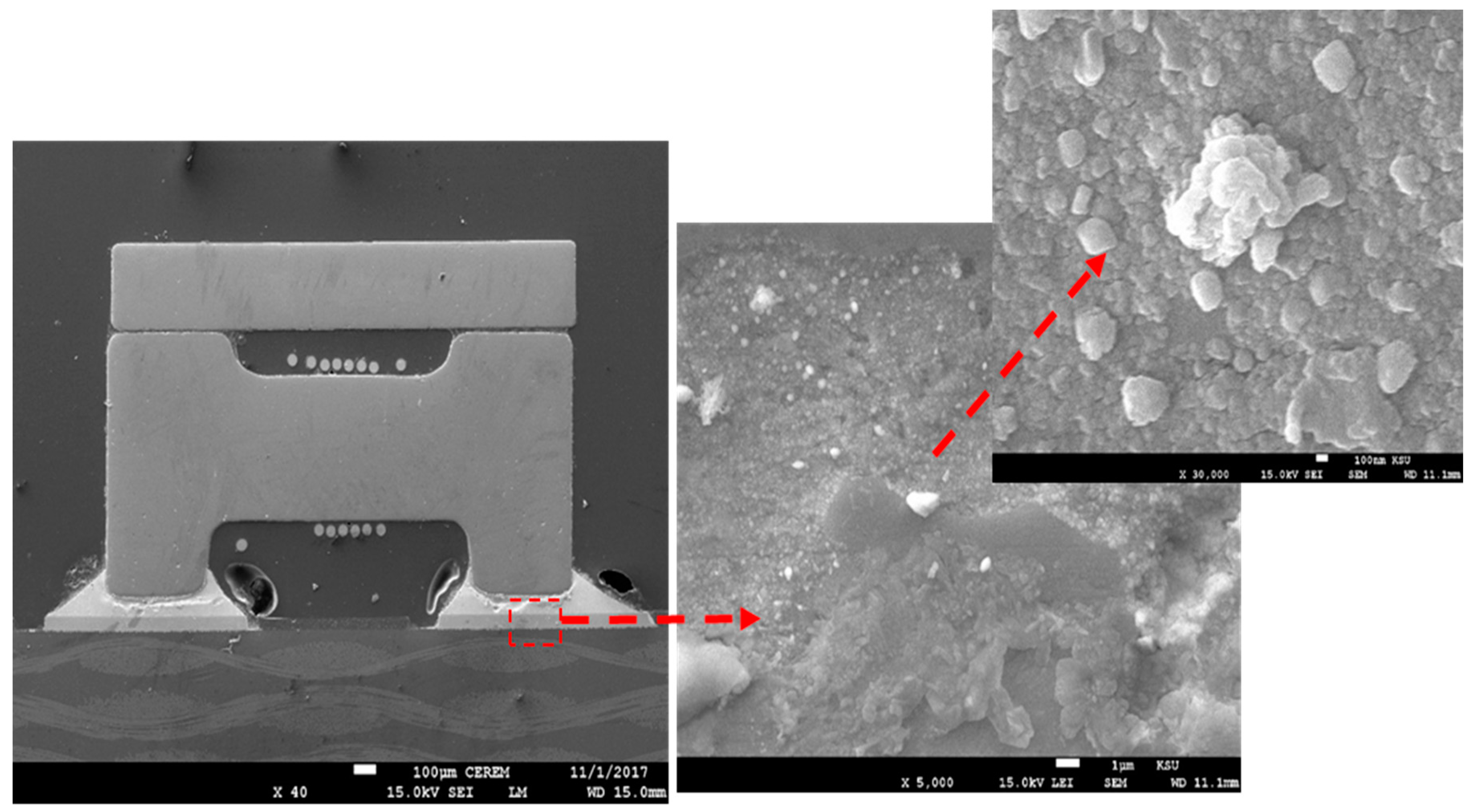
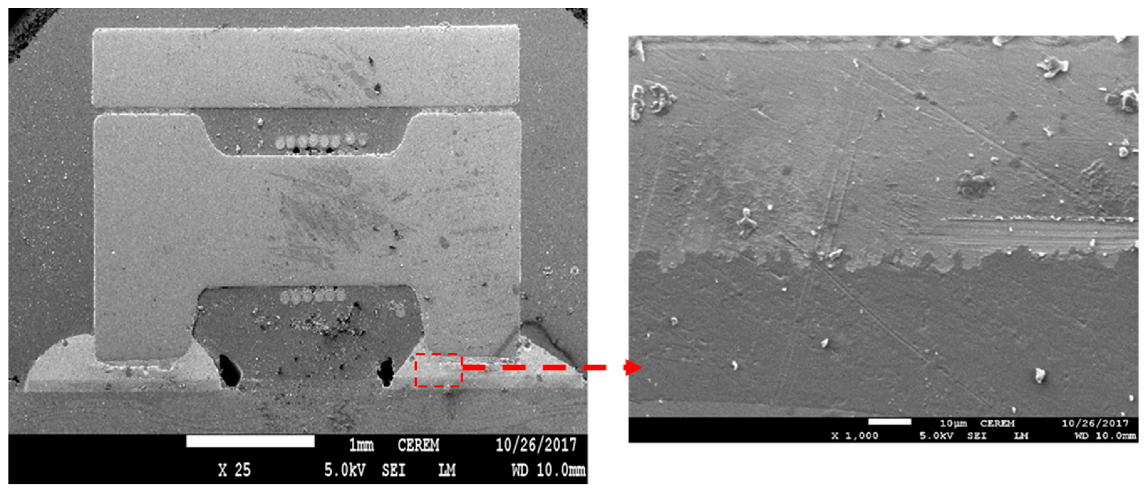
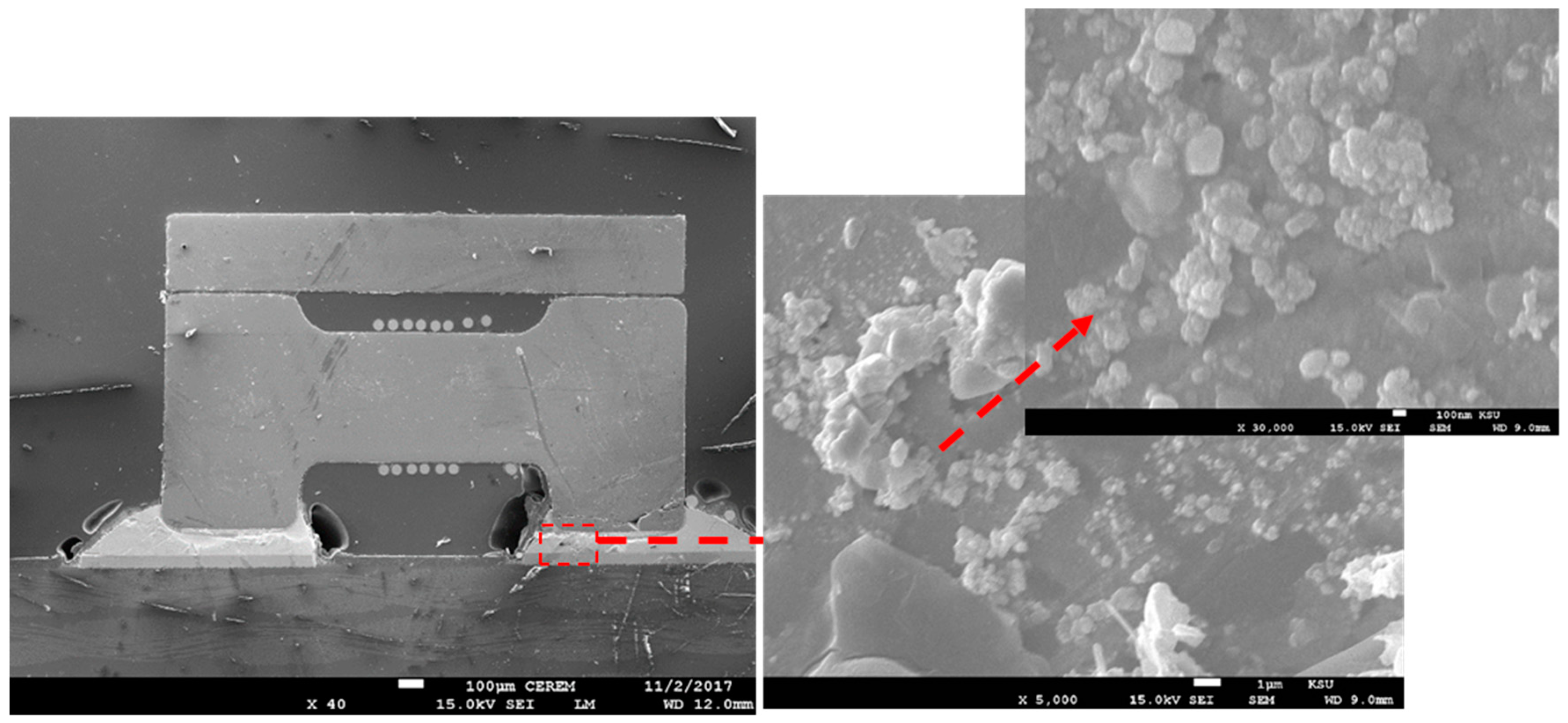
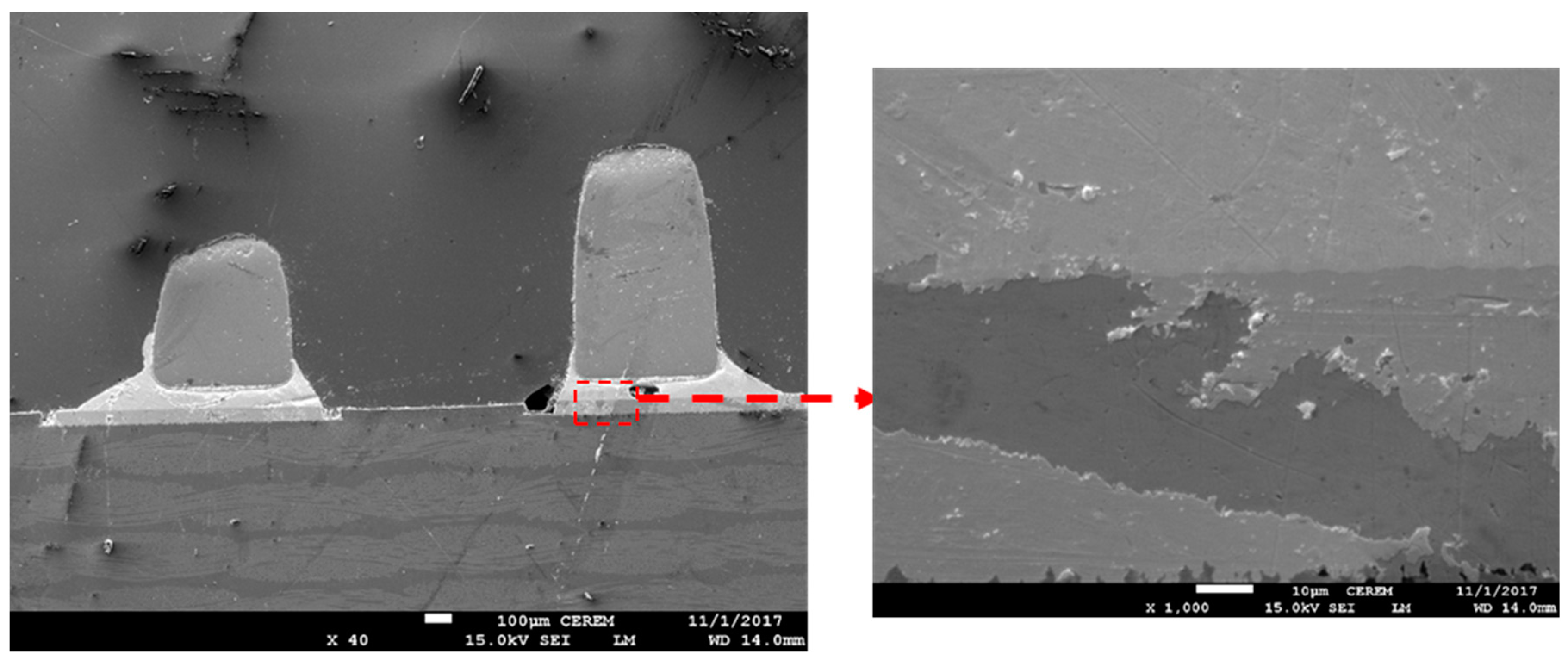
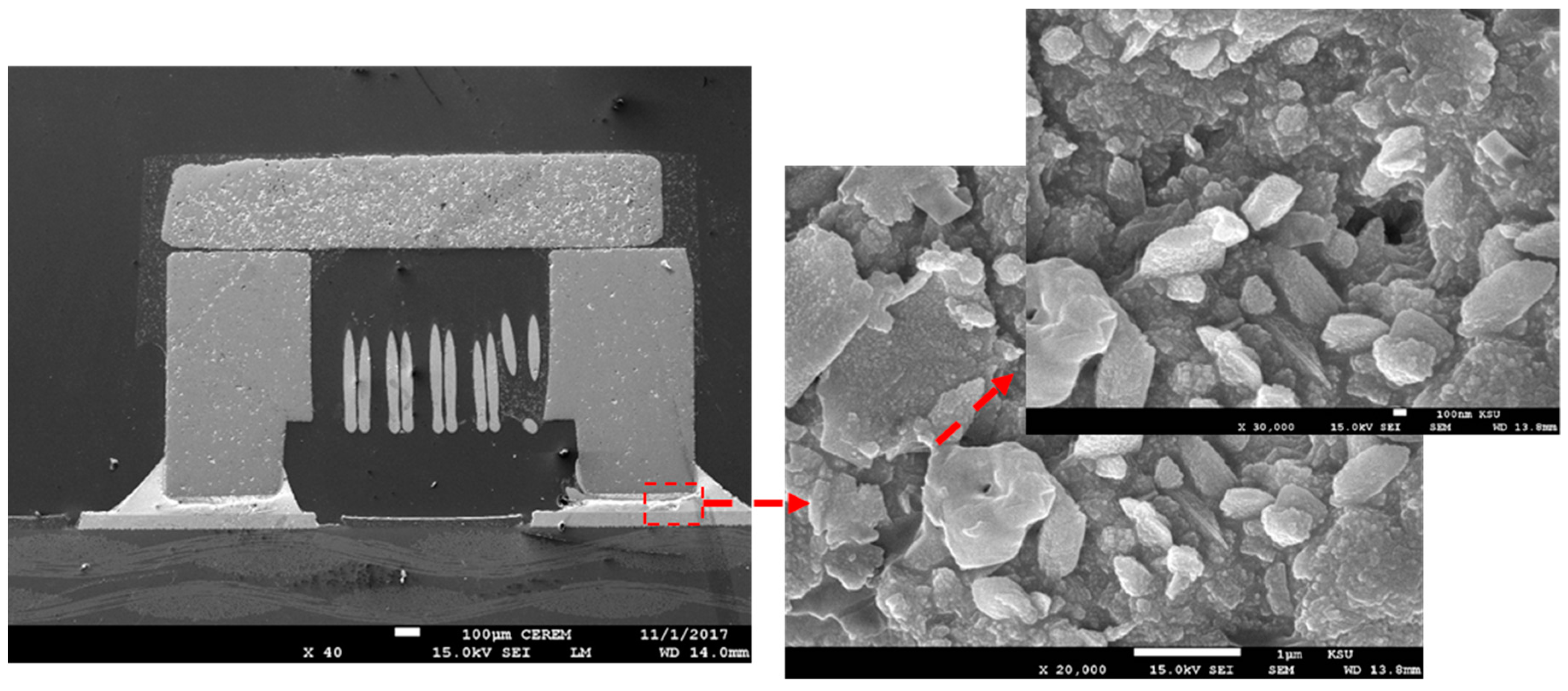
3.1. Microstructural Analysis
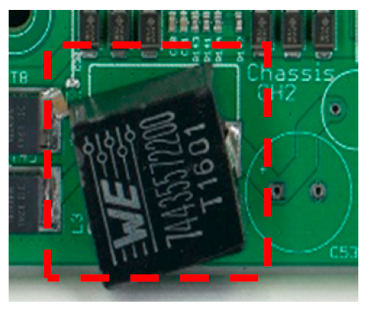
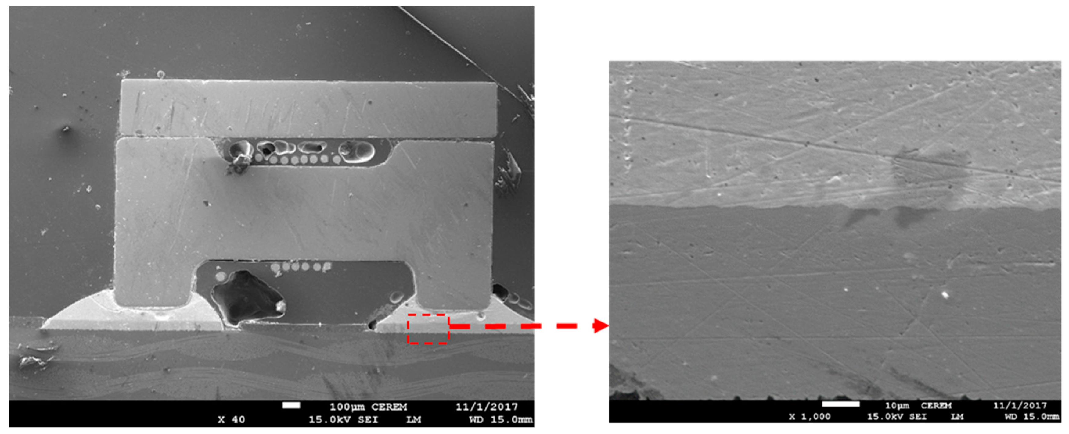
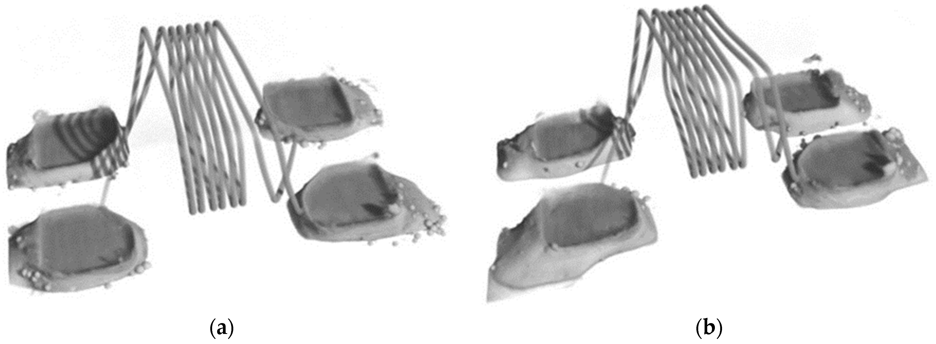
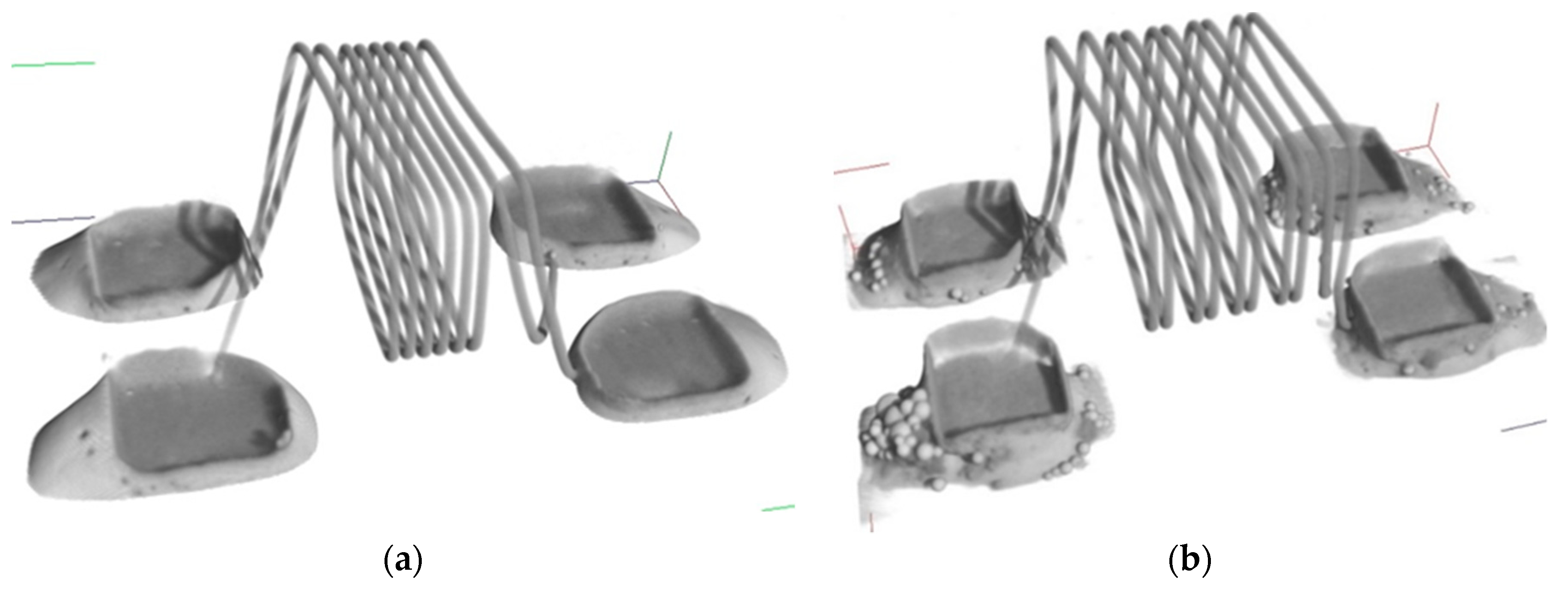
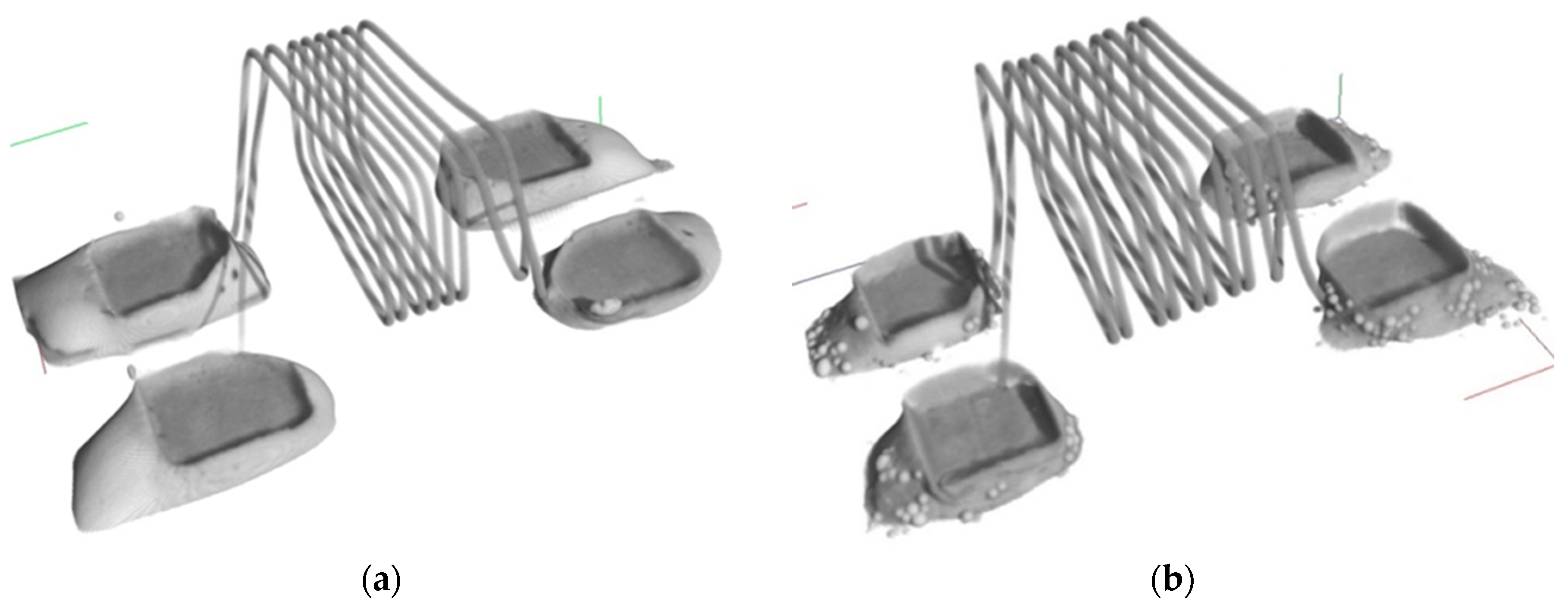
3.2. CT Scan Analysis
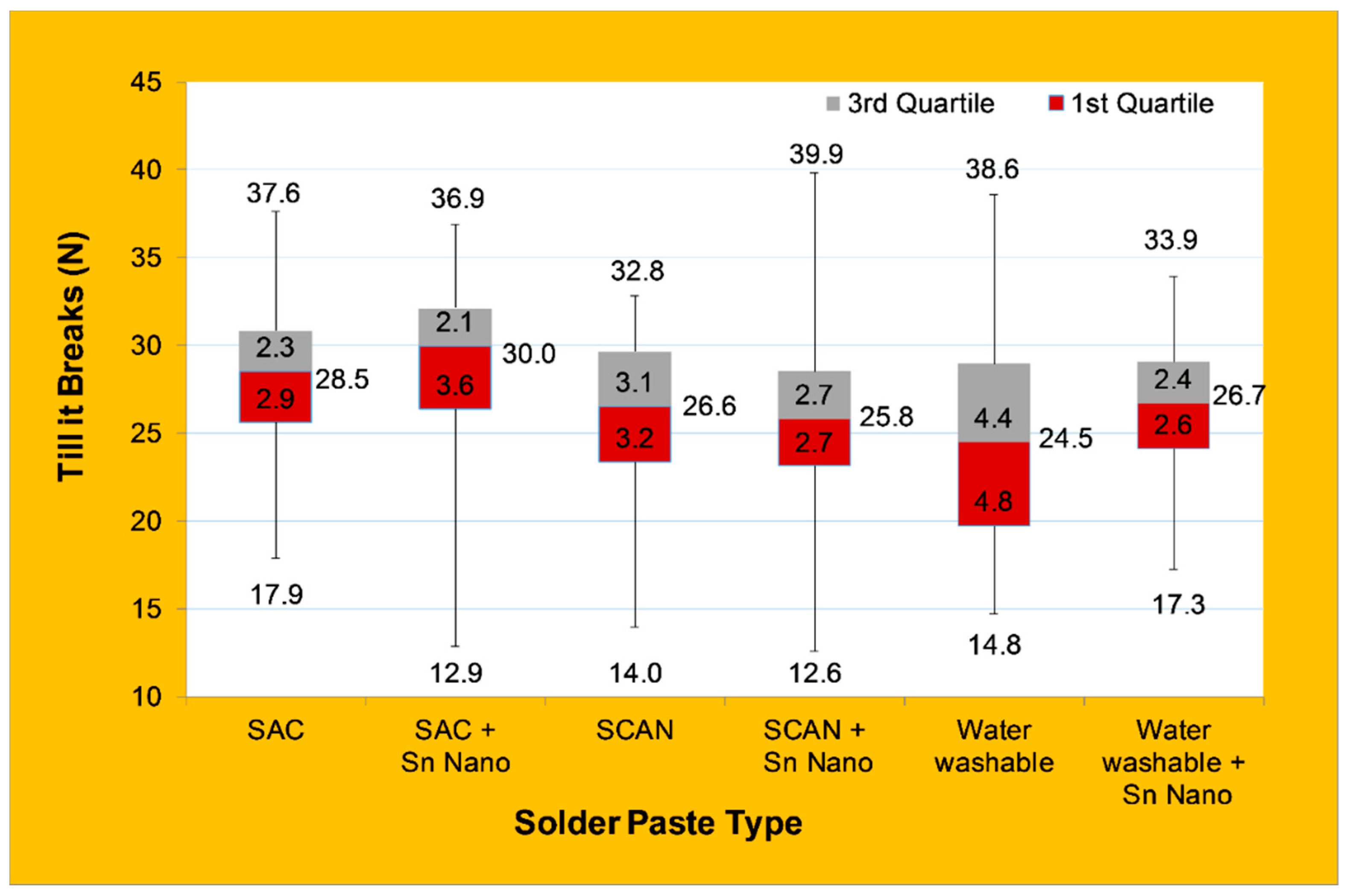
3.3. Evaluation of Joint Strength
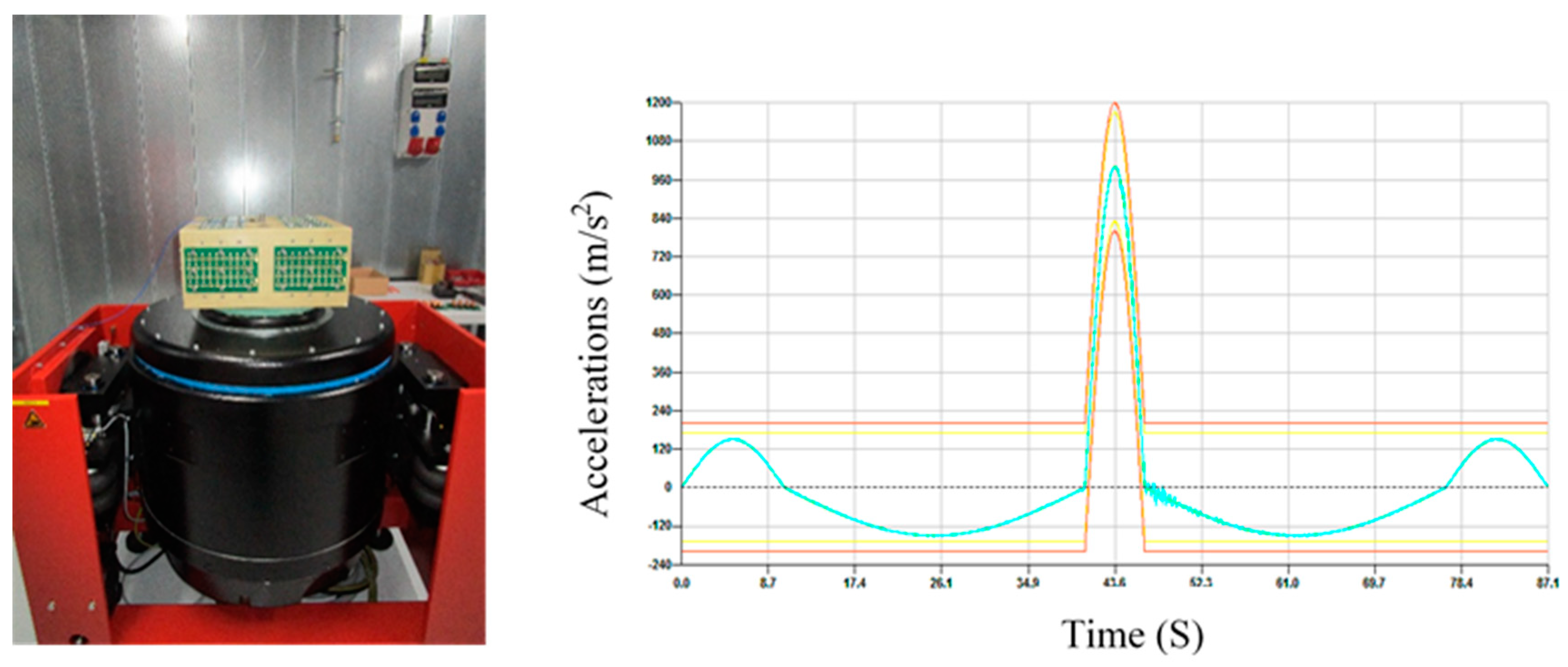
3.4. Mechanical Shock
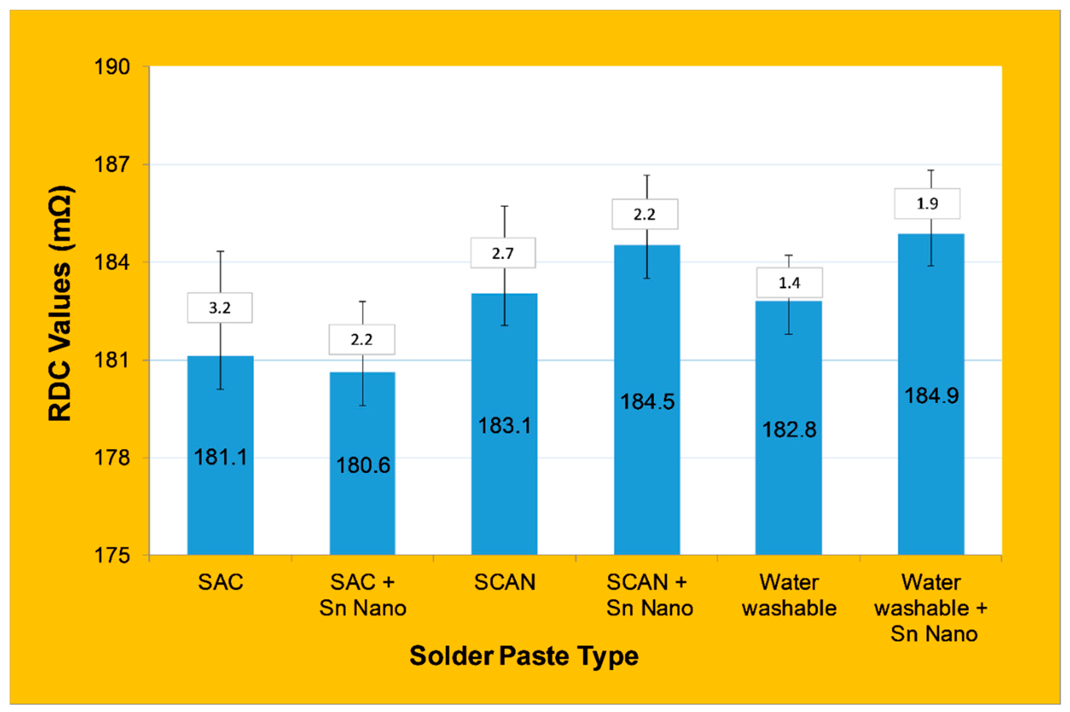
3.5. Electrical Resistivity Measurement
4. Conclusions
Author Contributions
Funding
Acknowledgments
Conflicts of Interest
References
- Baumli, P. Solder Materials With Micro And Nanoparticles: A Review. Mater. Sci. Eng. 2015, 40, 42–49. [Google Scholar]
- Fathian, Z.; Maleki, A.; Niroumand, B. Synthesis and characterization of ceramic nanoparticles reinforced lead-free solder. Ceram. Int. 2017, 43, 5302–5310. [Google Scholar] [CrossRef]
- Wierzbicka-Miernik, A.; Guspiel, J.; Zabdyr, L. Corrosion behavior of lead-free SAC-type solder alloys in liquid media. Arch. Civ. Mech. Eng. 2015, 15, 206–213. [Google Scholar] [CrossRef]
- Chellvarajoo, S.; Abdullah, M.Z. Investigation on nano-reinforced solder paste after reflow soldering part 1: Effects of nano-reinforced solder paste on melting, hardness, spreading rate, and wetting quality. Microelectron. Reliab. 2018, 84, 230–237. [Google Scholar] [CrossRef]
- Tan, A.T.; Tan, A.W.; Yusof, F. Evolution of microstructure and mechanical properties of Cu/SAC305/Cu solder joints under the influence of low ultrasonic power. J. Alloys Compd. 2017, 705, 188–197. [Google Scholar] [CrossRef]
- Freitas, E.S.; Osório, W.R.; Spinelli, J.E.; Garcia, A. Microelectronics Reliability Mechanical and corrosion resistances of a Sn—0.7 wt.% Cu lead-free solder alloy. Microelectron. Reliab. 2014, 54, 1392–1400. [Google Scholar] [CrossRef]
- Chen, G.; Peng, H.; Silberschmidt, V.V.; Chan, Y.C.; Liu, C.; Wu, F. Performance of Sn-3.0Ag-0.5Cu composite solder with TiC reinforcement: Physical properties, solderability and microstructural evolution under isothermal ageing. J. Alloys Compd. 2016, 685, 680–689. [Google Scholar] [CrossRef]
- Zhang, L.; Tu, K.N. Structure and properties of lead-free solders bearing micro and nano particles. Mater. Sci. Eng. 2014, 82, 1–32. [Google Scholar] [CrossRef]
- Chellvarajoo, S.; Abdullah, M.Z.; Samsudin, Z. Effects of Fe2NiO4 nanoparticles addition into lead free Sn–3.0Ag–0.5Cu solder pastes on microstructure and mechanical properties after reflow soldering process. Mater. Des. 2015, 67, 197–208. [Google Scholar] [CrossRef]
- Chellvarajoo, S.; Abdullah, M.Z. Microstructure and mechanical properties of Pb-free Sn–3.0Ag–0.5Cu solder pastes added with NiO nanoparticles after reflow soldering process. Mater. Des. J. 2016, 90, 499–507. [Google Scholar] [CrossRef]
- Amagai, M. A study of nanoparticles in Sn-Ag based lead free solders. Microelectron. Reliab. 2008, 48, 1–16. [Google Scholar] [CrossRef]
- Sharma, A.; Das, S.; Das, K. Electrochemical corrosion behavior of CeO2 nanoparticle reinforced Sn-Ag based lead free nanocomposite solders in 3.5wt.% NaCl bath. Surf. Coat. Technol. 2015, 261, 235–243. [Google Scholar] [CrossRef]
- Pan, Y.C.; Huang, W.F.; Li, G.Y.; Tang, Y.; Luo, S.M. Effects of Mn nanoparticles on tensile properties of low-Ag Sn-0.3Ag-0.7Cu-xMn solder alloys and joints. J. Alloys Compd. 2017, 719, 365–375. [Google Scholar]
- Hammad, A.E.; Ibrahiem, A.A. Enhancing the microstructure and tensile creep resistance of Sn-3.0Ag-0.5Cu solder alloy by reinforcing nano-sized ZnO particles. Microelectron. Reliab. 2017, 75, 187–194. [Google Scholar] [CrossRef]
- Chellvarajoo, S.; Abdullah, M.Z.; Khor, C.Y. Effects of diamond nanoparticles reinforcement into lead-free Sn-3.0Ag-0.5Cu solder pastes on microstructure and mechanical properties after reflow soldering process. Mater. Des. 2015, 82, 206–215. [Google Scholar] [CrossRef]
- Khodabakhshi, F.; Sayyadi, R.; Javid, N.S. Lead free Sn-Ag-Cu solders reinforced by Ni-coated graphene nanosheets prepared by mechanical alloying: Microstructural evolution and mechanical durability. Mater. Sci. Eng. 2017, 702, 371–385. [Google Scholar] [CrossRef]
- Chen, G.; Wu, F.; Liu, C.; Silberschmidt, V.V.; Chan, Y.C. Microstructures and properties of new Sn-Ag-Cu lead-free solder reinforced with Ni-coated graphene nanosheets. J. Alloys Compd. 2016, 656, 500–509. [Google Scholar] [CrossRef]


| Solder Paste-Type | Weight% (w.t.%) | ||||
|---|---|---|---|---|---|
| Sn | Cu | Ag | Ni | Ge | |
| SAC (SAC3-X(H)F3+-T3) | 96.50 | 0.50 | 3.00 | 0.00 | 0.00 |
| SCAN (SCAN-Ge071-XF3+-T3) | 98.45 | 0.60 | 0.90 | 0.04 | 0.01 |
| Water washable (P-AQ-SAC3-WW50-X121-T4) | 96.50 | 0.50 | 3.00 | 0.00 | 0.00 |
© 2019 by the authors. Licensee MDPI, Basel, Switzerland. This article is an open access article distributed under the terms and conditions of the Creative Commons Attribution (CC BY) license (http://creativecommons.org/licenses/by/4.0/).
Share and Cite
Atieh, A.M.; Abedalaziz, T.J.; AlHazaa, A.; Weser, M.; Al-Kouz, W.G.; Sari, M.S.; Alhoweml, I. Soldering of Passive Components Using Sn Nanoparticle Reinforced Solder Paste: Influence on Microstructure and Joint Strength. Nanomaterials 2019, 9, 1478. https://doi.org/10.3390/nano9101478
Atieh AM, Abedalaziz TJ, AlHazaa A, Weser M, Al-Kouz WG, Sari MS, Alhoweml I. Soldering of Passive Components Using Sn Nanoparticle Reinforced Solder Paste: Influence on Microstructure and Joint Strength. Nanomaterials. 2019; 9(10):1478. https://doi.org/10.3390/nano9101478
Chicago/Turabian StyleAtieh, Anas M., Tala J. Abedalaziz, Abdulaziz AlHazaa, Michael Weser, Wael G. Al-Kouz, Maen S. Sari, and Ibrahim Alhoweml. 2019. "Soldering of Passive Components Using Sn Nanoparticle Reinforced Solder Paste: Influence on Microstructure and Joint Strength" Nanomaterials 9, no. 10: 1478. https://doi.org/10.3390/nano9101478
APA StyleAtieh, A. M., Abedalaziz, T. J., AlHazaa, A., Weser, M., Al-Kouz, W. G., Sari, M. S., & Alhoweml, I. (2019). Soldering of Passive Components Using Sn Nanoparticle Reinforced Solder Paste: Influence on Microstructure and Joint Strength. Nanomaterials, 9(10), 1478. https://doi.org/10.3390/nano9101478