A Thin Film Flexible Supercapacitor Based on Oblique Angle Deposited Ni/NiO Nanowire Arrays

 , ,
, ,
Abstract

1. Introduction
2. Materials and Methods
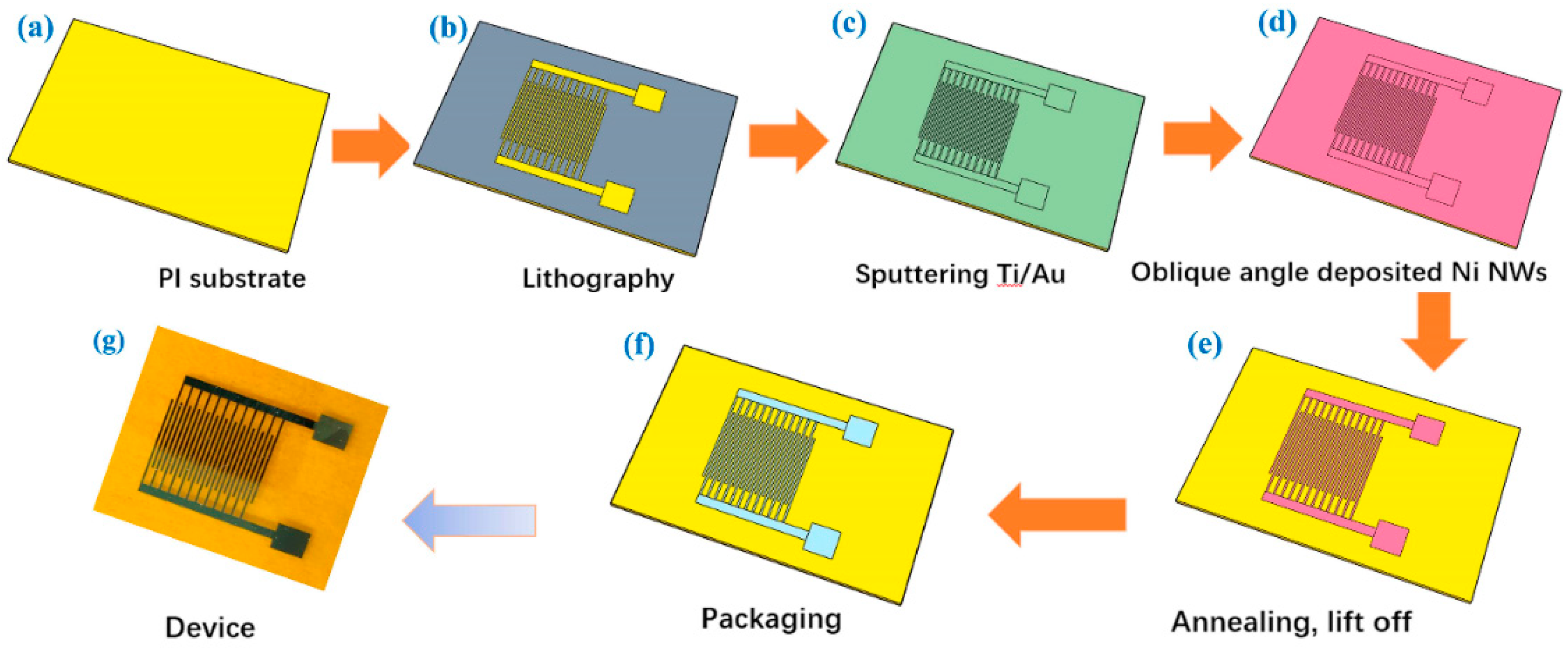
2.1. NiO Nanowires-Based MSC Growth Process
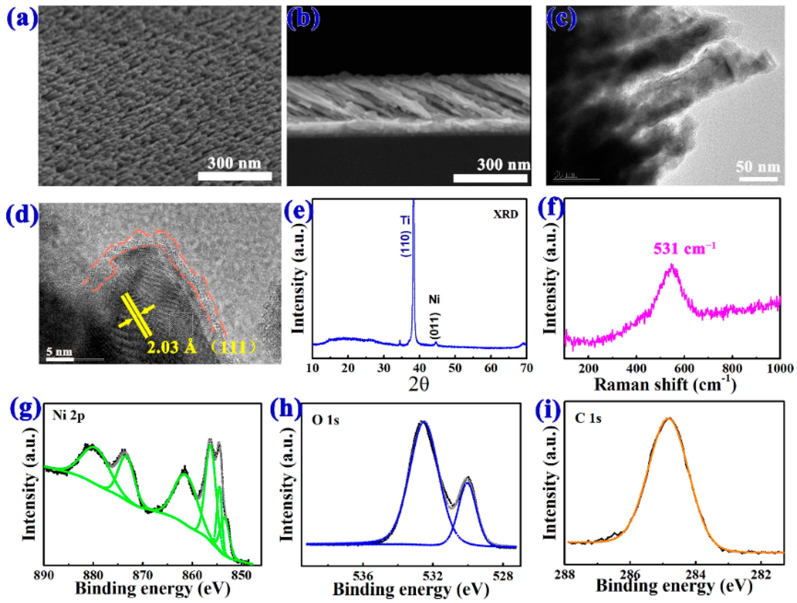
2.2. Materials Characterization
2.3. Calculation
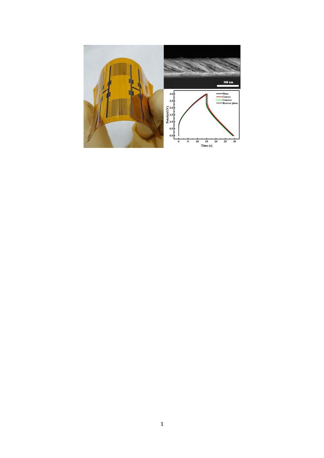
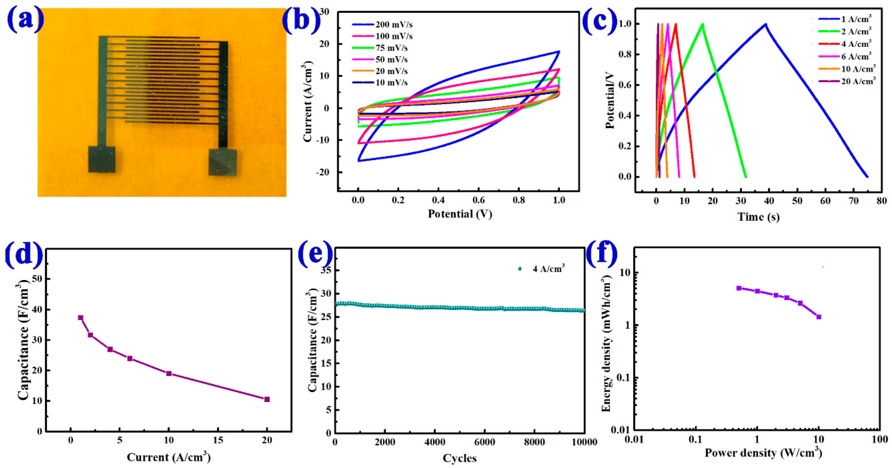
3. Results
4. Conclusions
Supplementary Materials
Author Contributions
Acknowledgments
Conflicts of Interest
References
- Simon, P.; Gogotsi, Y.; Dunn, B. Where do batteries end and supercapacitors begin? Science 2014, 343, 1210–1211. [Google Scholar] [CrossRef] [PubMed]
- Aricò, A.S.; Bruce, P.; Scrosati, B.; Tarascon, J.-M.; van Schalkwijk, W. Nanostructured materials for advanced energy conversion and storage devices. Nat. Mater. 2005, 4, 366. [Google Scholar] [CrossRef] [PubMed]
- Wang, Y.; Xia, Y. Recent progress in supercapacitors: From materials design to system construction. Adv. Mater. 2013, 25, 5336–5342. [Google Scholar] [CrossRef] [PubMed]
- Wang, Y.; Song, Y.; Xia, Y. Electrochemical capacitors: Mechanism, materials, systems, characterization and applications. Chem. Soc. Rev. 2016, 45, 5925–5950. [Google Scholar] [CrossRef] [PubMed]
- Huang, Y.; Zhu, M.; Huang, Y.; Pei, Z.; Li, H.; Wang, Z.; Xue, Q.; Zhi, C. Multifunctional energy storage and conversion devices. Adv. Mater. 2016, 28, 8344–8364. [Google Scholar] [CrossRef] [PubMed]
- Meng, Q.; Wu, H.; Meng, Y.; Xie, K.; Wei, Z.; Guo, Z. High-performance all-carbon yarn micro-supercapacitor for an integrated energy system. Adv. Mater. 2014, 26, 4100–4106. [Google Scholar] [CrossRef] [PubMed]
- Dong, X.; Guo, Z.; Song, Y.; Hou, M.; Wang, J.; Wang, Y.; Xia, Y. Flexible and wire-shaped micro-supercapacitor based on Ni(OH)2-nanowire and ordered mesoporous carbon electrodes. Adv. Funct. Mater. 2014, 24, 3405–3412. [Google Scholar] [CrossRef]
- Guo, K.; Wan, Y.; Yu, N.; Hu, L.; Zhai, T.; Li, H. Hand-drawing patterned ultra-thin integrated electrodes for flexible micro supercapacitors. Energy Storage Mater. 2018, 11, 144–151. [Google Scholar] [CrossRef]
- Liu, N.; Gao, Y. Recent progress in micro-supercapacitors with in-plane interdigital electrode architecture. Small 2017, 13. [Google Scholar] [CrossRef] [PubMed]
- Wang, C.; Zhou, E.; He, W.; Deng, X.; Huang, J.; Ding, M.; Wei, X.; Liu, X.; Xu, X. NiCo2O4-based supercapacitor nanomaterials. Nanomaterials 2017, 7, 41. [Google Scholar] [CrossRef] [PubMed]
- Xu, J.; Wu, H.; Lu, L.; Leung, S.-F.; Chen, D.; Chen, X.; Fan, Z.; Shen, G.; Li, D. Integrated photo-supercapacitor based on Bi-polar TiO2 nanotube arrays with selective one-side plasma-assisted hydrogenation. Adv. Funct. Mater. 2014, 24, 1840–1846. [Google Scholar] [CrossRef]
- Wu, H.; Jiang, K.; Gu, S.; Yang, H.; Lou, Z.; Chen, D.; Shen, G. Two-dimensional Ni(OH)2 nanoplates for flexible on-chip microsupercapacitors. Nano Res. 2015, 8, 3544–3552. [Google Scholar] [CrossRef]
- Barranco, A.; Borras, A.; Gonzalez-Elipe, A.R.; Palmero, A. Perspectives on oblique angle deposition of thin films: From fundamentals to devices. Prog. Mater. Sci. 2016, 76, 59–153. [Google Scholar] [CrossRef]
- Martín-Tovar, E.A.; Denis-Alcocer, E.; Chan y Díaz, E.; Castro-Rodríguez, R.; Iribarren, A. Tuning of refractive index in Al-doped ZnO films by rf-sputtering using oblique angle deposition. J. Phys. D Appl. Phys. 2016, 49, 295302. [Google Scholar] [CrossRef]
- Nuchuay, P.; Chaikeeree, T.; Kasayapanand, N.; Mungkung, N.; Arunrungrusmi, S.; Horprathum, M.; Eiamchai, P.; Limwichean, S.; Patthanasettakul, V.; Nuntawong, N.; et al. Preparation and characterization of ito nanostructure by oblique angle deposition. Mater. Today Proc. 2017, 4, 6284–6288. [Google Scholar] [CrossRef]
- Kannan, V.; Inamdar, A.I.; Pawar, S.M.; Kim, H.S.; Park, H.C.; Kim, H.; Im, H.; Chae, Y.S. Facile route to NiO nanostructured electrode grown by oblique angle deposition technique for supercapacitors. ACS Appl. Mater. Interfaces 2016, 8, 17220–17225. [Google Scholar] [CrossRef] [PubMed]
- Gu, S.; Lou, Z.; Li, L.; Chen, Z.; Ma, X.; Shen, G. Fabrication of flexible reduced graphene oxide/Fe2O3 hollow nanospheres based on-chip micro-supercapacitors for integrated photodetecting applications. Nano Res. 2015, 9, 424–434. [Google Scholar] [CrossRef]
- Wu, H.; Lou, Z.; Yang, H.; Shen, G. A flexible spiral-type supercapacitor based on ZnCo2O4 nanorod electrodes. Nanoscale 2015, 7, 1921–1926. [Google Scholar] [CrossRef] [PubMed]
- Ai, Y.; Geng, X.; Lou, Z.; Wang, Z.M.; Shen, G. Rational synthesis of branched CoMoM4@CoNiO2 core/shell nanowire arrays for all-solid-state supercapacitors with improved performance. ACS Appl. Mater. Interfaces 2015, 7, 24204–24211. [Google Scholar] [CrossRef] [PubMed]
- Hawkeye, M.M.; Brett, M.J. Glancing angle deposition: Fabrication, properties, and applications of micro- and nanostructured thin films. J. Vac. Sci. Technol. A Vac. Surf. Films 2007, 25, 1317. [Google Scholar] [CrossRef]
- Karabacak, T.; Wang, G.C.; Lu, T.M. Physical self-assembly and the nucleation of three-dimensional nanostructures by oblique angle deposition. J. Vac. Sci. Technol. A Vac. Surf. Films 2004, 22, 1778–1784. [Google Scholar] [CrossRef]
- Malac, M.; Egerton, R.F. Observations of the microscopic growth mechanism of pillars and helices formed by glancing-angle thin-film deposition. J. Vac. Sci. Technol. A Vac. Surf. Films 2001, 19, 158–166. [Google Scholar] [CrossRef]
- Torrisi, V.; Ruffino, F. Nanoscale structure of submicron-thick sputter-deposited Pd films: Effect of the adatoms diffusivity by the film-substrate interaction. Surf. Coat. Technol. 2017, 315, 123–129. [Google Scholar] [CrossRef]
- Ruffino, F.; Torrisi, V.; Marletta, G.; Grimaldi, M.G. Atomic force microscopy investigation of the kinetic growth mechanisms of sputtered nanostructured Au film on mica: Towards a nanoscale morphology control. Nanoscale Res. Lett. 2011, 6, 112. [Google Scholar] [CrossRef] [PubMed]
- Ruffino, F.; Crupi, I.; Irrera, A.; Grimaldi, M.G. Pd/Au/SiC nanostructured diodes for nanoelectronics: Room temperature electrical properties. IEEE Trans. Nanotechnol. 2010, 9, 414–421. [Google Scholar] [CrossRef]
- Zhang, L.; Cosandey, F.; Persaud, R.; Madey, T.E. Initial growth and morphology of thin Au films on TiO2(110). Surf. Sci. 1999, 439, 73–85. [Google Scholar] [CrossRef]
- Prudêncio, L.M.; Paramês, L.; Conde, O.; da Silva, R.C. Cr ion implantation into ti. Surf. Coat. Technol. 2006, 200, 3907–3912. [Google Scholar] [CrossRef]
- Mi, Y.; Yuan, D.; Liu, Y.; Zhang, J.; Xiao, Y. Synthesis of hexagonal close-packed nanocrystalline nickel by a thermal reduction process. Mater. Chem. Phys. 2005, 89, 359–361. [Google Scholar] [CrossRef]
- Yan, H.; Zhang, D.; Xu, J.; Lu, Y.; LiuYan, H.; Zhang, D.; Xu, J.; Lu, Y.; Liu, Y.; Qiu, K.; Zhang, Y.; Luo, Y. Solution growth of NiO nanosheets supported on Ni foam as high-performance electrodes for supercapacitors. Nanoscale Res. Lett. 2014, 9, 424. [Google Scholar] [CrossRef] [PubMed]
- Qiu-Lin, N.I.E.; Hong-Ting, Z.; Hao-Yong, Y.I.N.; Zhen-Zhen, C.U.I. Preparation and glucose sensing property of core-shelled nikel oxide/carbon microspheres. J. Inorg. Mater. 2015, 30, 305. [Google Scholar]
- Wu, Z.S.; Parvez, K.; Feng, X.; Mullen, K. Graphene-based in-plane micro-supercapacitors with high power and energy densities. Nat. Commun. 2013, 4, 2487. [Google Scholar] [CrossRef] [PubMed]
- Guan, C.; Wang, Y.; Hu, Y.; Liu, J.; Ho, K.H.; Zhao, W.; Fan, Z.; Shen, Z.; Zhang, H.; Wang, J. Conformally deposited NiO on a hierarchical carbon support for high-power and durable asymmetric supercapacitors. J. Mater. Chem. A 2015, 3, 23283–23288. [Google Scholar] [CrossRef]
- Oswald, S.; Brückner, W. Xps depth profile analysis of non-stoichiometric NiO films. Surf. Interface Anal. 2004, 36, 17–22. [Google Scholar] [CrossRef]
- Guan, C.; Wang, Y.; Zacharias, M.; Wang, J.; Fan, H.J. Atomic-layer-deposition alumina induced carbon on porous NixCo1-xO nanonets for enhanced pseudocapacitive and Li-ion storage performance. Nanotechnology 2015, 26, 014001. [Google Scholar] [CrossRef] [PubMed]
- Varghese, B.; Reddy, M.V.; Yanwu, Z.; Lit, C.S.; Hoong, T.C.; Subba Rao, G.V.; Chowdari, B.V.R.; Wee, A.T.S.; Lim, C.T.; Sow, C.-H. Fabrication of NiO nanowall electrodes for high performance lithium ion battery. Chem. Mater. 2008, 20, 3360–3367. [Google Scholar] [CrossRef]
- Wang, H.-Q.; Fan, X.-P.; Zhang, X.-H.; Huang, Y.-G.; Wu, Q.; Pan, Q.-C.; Li, Q.-Y. In situ growth of NiO nanoparticles on carbon paper as a cathode for rechargeable Li-O2 batteries. RSC Adv. 2017, 7, 23328–23333. [Google Scholar] [CrossRef]
- Chen, C.; Chen, C.; Huang, P.; Duan, F.; Zhao, S.; Li, P.; Fan, J.; Song, W.; Qin, Y. NiO/nanoporous graphene composites with excellent supercapacitive performance produced by atomic layer deposition. Nanotechnology 2014, 25, 504001. [Google Scholar] [CrossRef] [PubMed]
- Ai, Y.; Lou, Z.; Chen, S.; Chen, D.; Wang, Z.M.; Jiang, K.; Shen, G. All RGO-on-PVDF-nanofibers based self-powered electronic skins. Nano Energy 2017, 35, 121–127. [Google Scholar] [CrossRef]


© 2018 by the authors. Licensee MDPI, Basel, Switzerland. This article is an open access article distributed under the terms and conditions of the Creative Commons Attribution (CC BY) license (http://creativecommons.org/licenses/by/4.0/).
Share and Cite
Ma, J.; Liu, W.; Zhang, S.; Ma, Z.; Song, P.; Yang, F.; Wang, X. A Thin Film Flexible Supercapacitor Based on Oblique Angle Deposited Ni/NiO Nanowire Arrays. Nanomaterials 2018, 8, 422. https://doi.org/10.3390/nano8060422
Ma J, Liu W, Zhang S, Ma Z, Song P, Yang F, Wang X. A Thin Film Flexible Supercapacitor Based on Oblique Angle Deposited Ni/NiO Nanowire Arrays. Nanomaterials. 2018; 8(6):422. https://doi.org/10.3390/nano8060422
Chicago/Turabian StyleMa, Jing, Wen Liu, Shuyuan Zhang, Zhe Ma, Peishuai Song, Fuhua Yang, and Xiaodong Wang. 2018. "A Thin Film Flexible Supercapacitor Based on Oblique Angle Deposited Ni/NiO Nanowire Arrays" Nanomaterials 8, no. 6: 422. https://doi.org/10.3390/nano8060422
APA StyleMa, J., Liu, W., Zhang, S., Ma, Z., Song, P., Yang, F., & Wang, X. (2018). A Thin Film Flexible Supercapacitor Based on Oblique Angle Deposited Ni/NiO Nanowire Arrays. Nanomaterials, 8(6), 422. https://doi.org/10.3390/nano8060422