Heavily Boron-Doped Silicon Layer for the Fabrication of Nanoscale Thermoelectric Devices

 ,
,  ,
,
Abstract
:
1. Introduction
2. Materials and Methods
3. Results and Discussion
3.1. Diffusion Depth of Boron
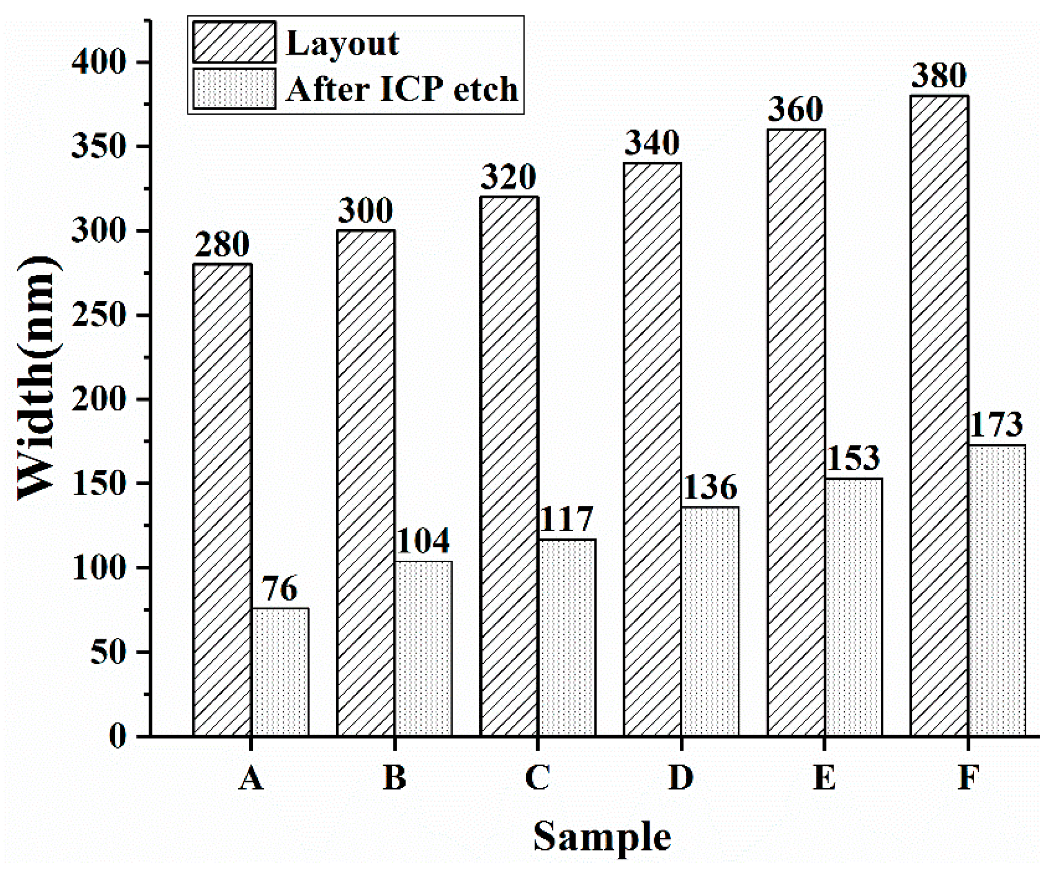
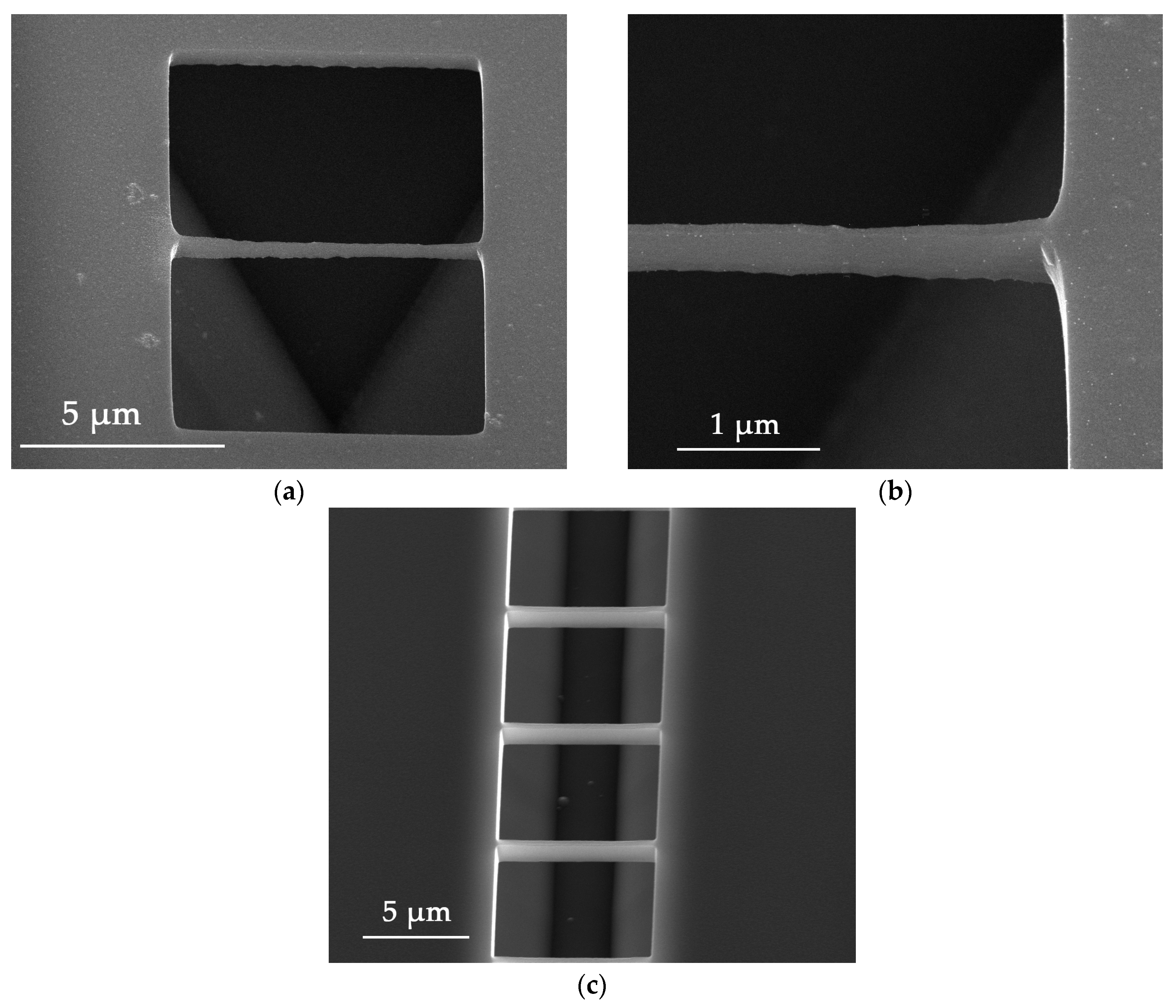
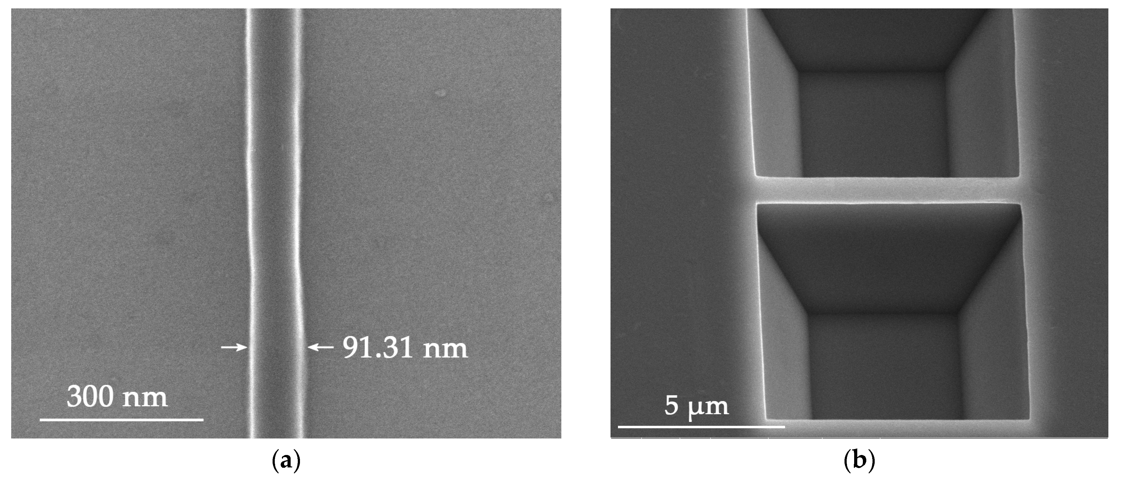
3.2. Electron Beam Lithography and ICP
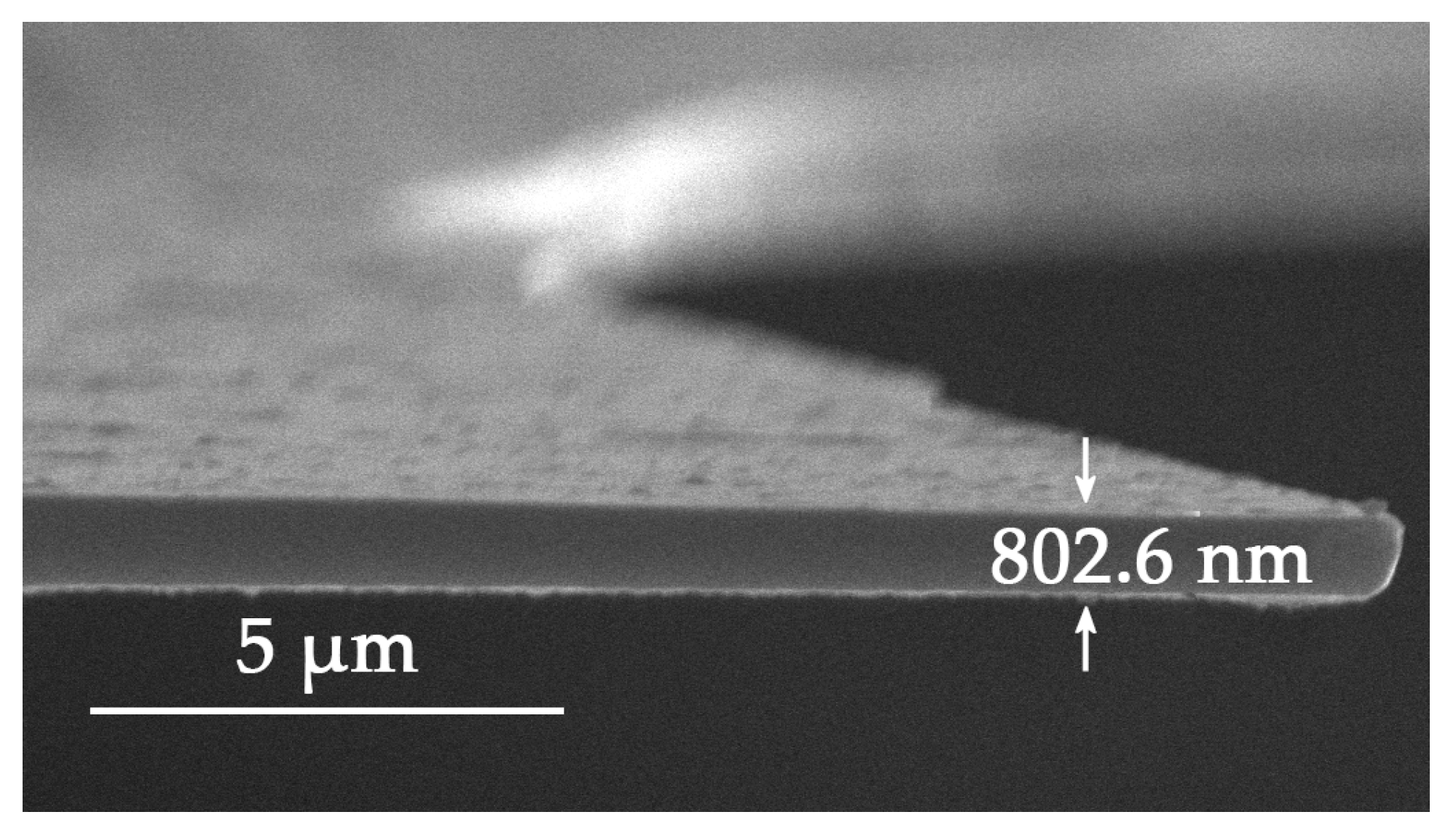
3.3. Suspending of the Nanowire
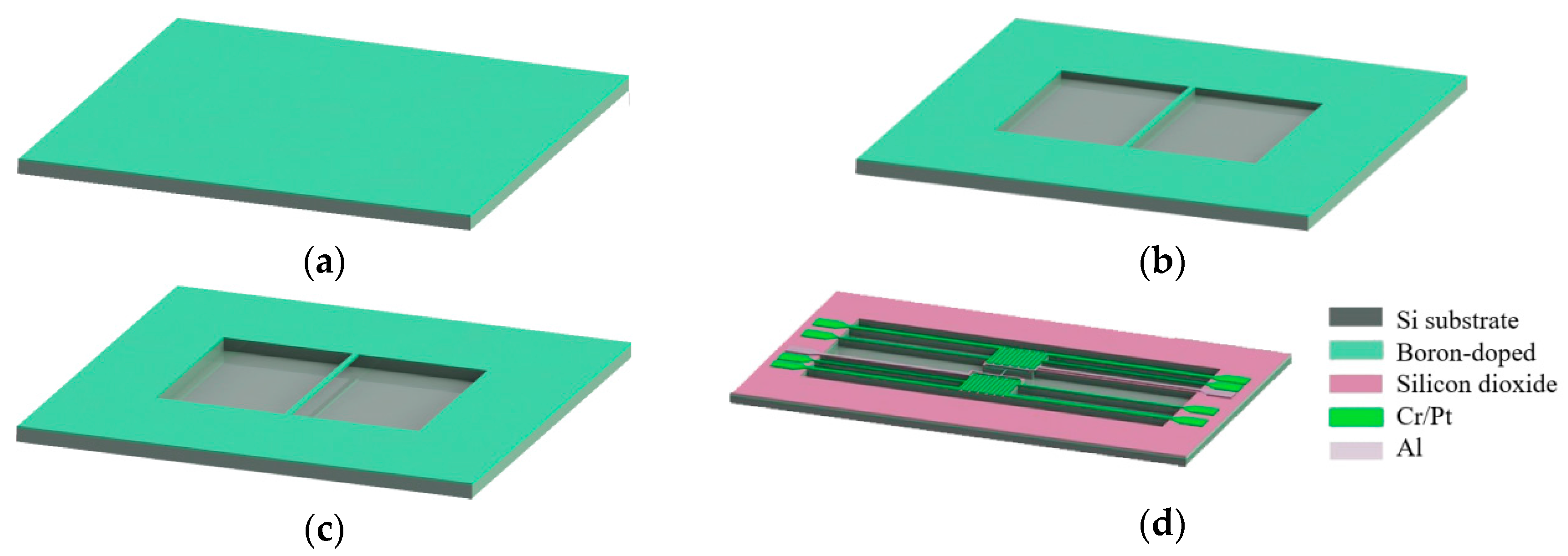
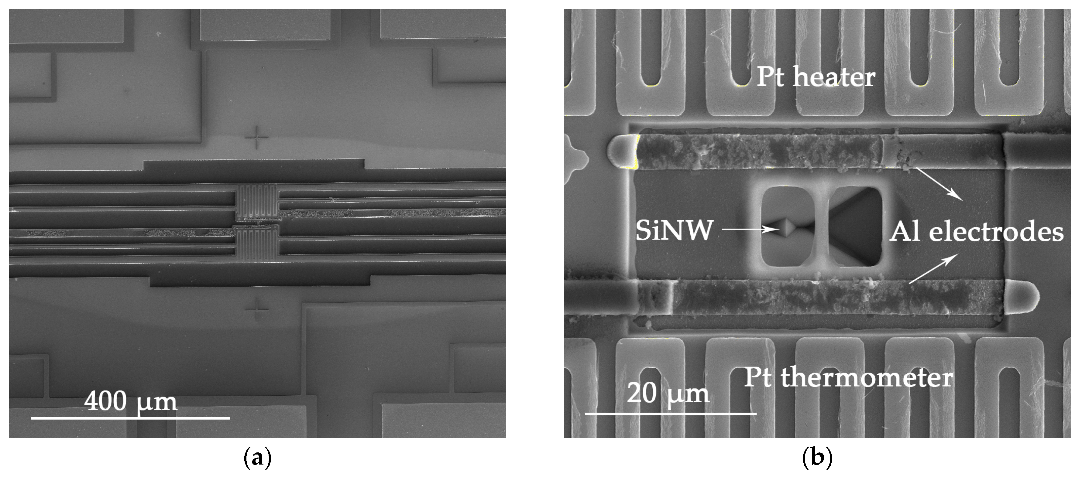
3.4. Fabrication of the Thermoelectric Device
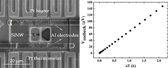
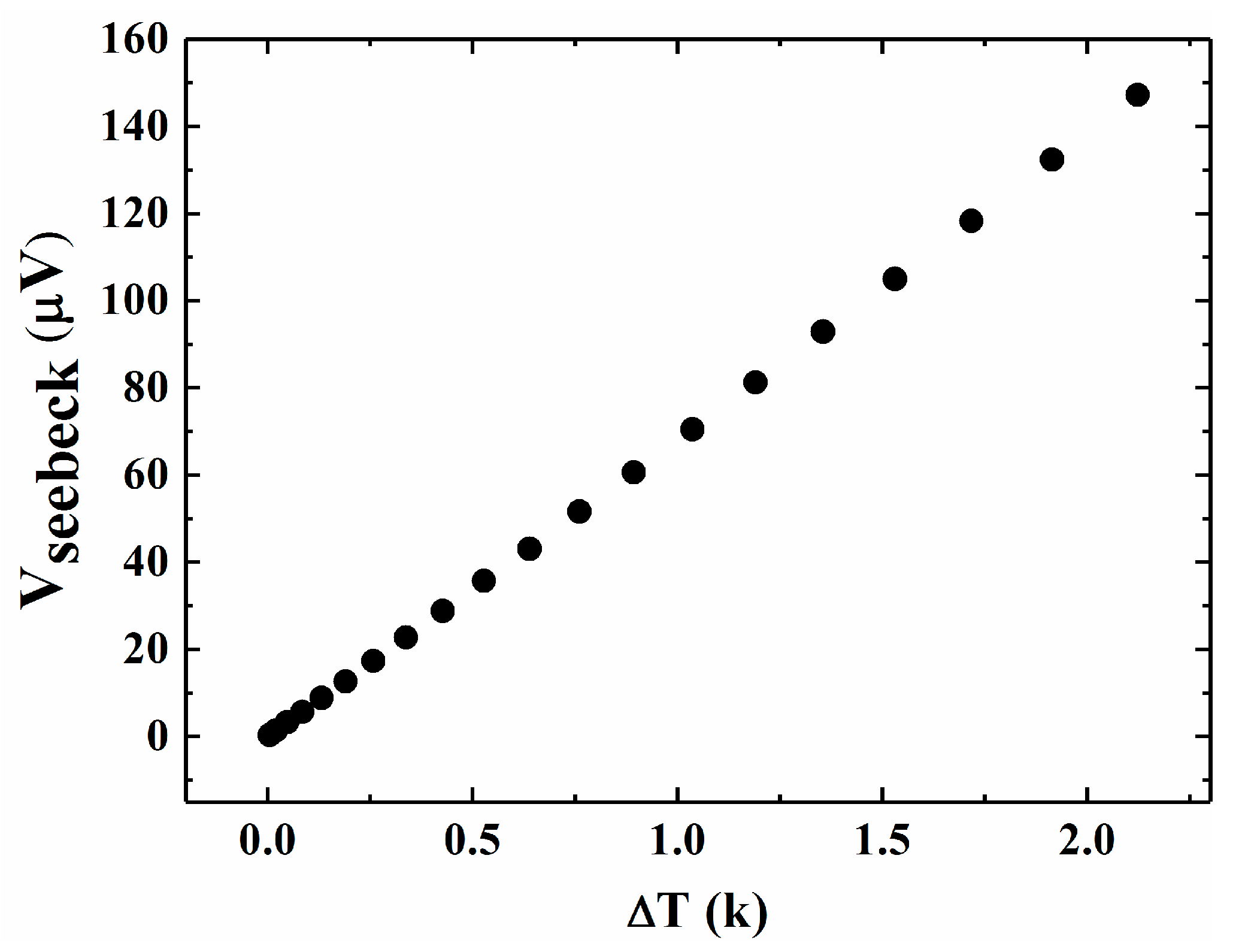
3.5. Characterization of the Thermoelectric Device
4. Conclusions
Acknowledgments
Author Contributions
Conflicts of Interest
References
- Vining, C.B. An inconvenient truth about thermoelectrics. Nat. Mater. 2009, 8, 83–85. [Google Scholar] [CrossRef] [PubMed]
- Heremans, J.P.; Dresselhaus, M.S.; Bell, L.E.; Morelli, D.T. When thermoelectrics reached the nanoscale. Nat. Nanotechnol. 2013, 8, 471–473. [Google Scholar] [CrossRef] [PubMed]
- Lee, J.; Lee, W.; Lim, J.; Yu, Y.; Kong, Q.; Urban, J.J.; Yang, P.D. Thermal transport in silicon nanowires at high temperature up to 700 k. Nano Lett. 2016, 16, 4133–4140. [Google Scholar] [CrossRef] [PubMed]
- Qi, Y.Y.; Wang, Z.; Zhang, M.L.; Yang, F.H.; Wang, X.D. Thermoelectric devices based on one-dimensional nanostructures. J. Mater. Chem. A 2013, 1, 6110–6124. [Google Scholar] [CrossRef]
- Hobbs, R.G.; Petkov, N.; Holmes, J.D. Semiconductor nanowire fabrication by bottom-up and top-down paradigms. Chem. Mater. 2012, 24, 1975–1991. [Google Scholar] [CrossRef]
- Wu, Y.; Yang, P. Germanium nanowire growth via simple vapor transport. Chem. Mater. 2000, 12, 605–607. [Google Scholar] [CrossRef]
- Johnson, D.C.; Mosby, J.M.; Riha, S.C.; Prieto, A.L. Synthesis of copper silicide nanocrystallites embedded in silicon nanowires for enhanced transport properties. J. Mater. Chem. 2010, 20, 1993–1998. [Google Scholar] [CrossRef]
- Holmes, J.D.; Johnston, K.P.; Doty, R.C.; Korgel, B.A. Control of thickness and orientation of solution-grown silicon nanowires. Science 2000, 287, 1471–1473. [Google Scholar] [CrossRef] [PubMed]
- Wang, F.; Dong, A.; Sun, J.; Tang, R.; Yu, H.; Buhro, W.E. Solution-liquid-solid growth of semiconductor nanowires. Inorg. Chem. 2006, 45, 7511–7521. [Google Scholar] [CrossRef] [PubMed]
- Cao, G.; Liu, D. Template-based synthesis of nanorod, nanowire, and nanotube arrays. Adv. Colloid Interface Sci. 2008, 136, 45–64. [Google Scholar] [CrossRef] [PubMed]
- Jang, M.; Park, Y.; Hyun, Y.; Jun, M.; Choi, S.-J.; Zyung, T.; Kim, J.-D. Top-down processed silicon nanowires for thermoelectric applications. J. Nanosci. Nanotechnol. 2012, 12, 3552–3554. [Google Scholar] [CrossRef] [PubMed]
- Qi, Y.Y.; Wang, Z.; Zhang, M.L.; Yang, F.H.; Wang, X.D. A processing window for fabricating heavily doped silicon nanowires by metal-assisted chemical etching. J. Phys. Chem. C 2013, 117, 25090–25096. [Google Scholar] [CrossRef]
- Liu, Y.; Sun, W.; Jiang, Y.; Zhao, X.-Z. Fabrication of bifacial wafer-scale silicon nanowire arrays with ultra-high aspect ratio through controllable metal-assisted chemical etching. Mater. Lett. 2015, 139, 437–442. [Google Scholar] [CrossRef]
- Boukai, A.I.; Bunimovich, Y.; Tahir-Kheli, J.; Yu, J.K.; Goddard, W.A.; Heath, J.R. Silicon nanowires as efficient thermoelectric materials. Nature 2008, 451, 168–171. [Google Scholar] [CrossRef] [PubMed]
- Hochbaum, A.I.; Chen, R.; Delgado, R.D.; Liang, W.; Garnett, E.C.; Najarian, M.; Majumdar, A.; Yang, P. Enhanced thermoelectric performance of rough silicon nanowires. Nature 2008, 451, 163–167. [Google Scholar] [CrossRef] [PubMed]
- Toriyama, T.; Sugiyama, S. Single crystal silicon piezoresistive nano-wire bridge. Sens. Actuators A Phys. 2003, 108, 244–249. [Google Scholar] [CrossRef]
- Koumela, A.; Mercier, D.; Dupre, C.; Jourdan, G.; Marcoux, C.; Ollier, E.; Purcell, S.T.; Duraffourg, L. Piezoresistance of top-down suspended si nanowires. Nanotechnology 2011, 22, 395701. [Google Scholar] [CrossRef] [PubMed]
- Zabah, N.F.; Kwa, K.S.K.; Bowen, L.; Mendis, B.; Oneill, A. Top-down fabrication of single crystal silicon nanowire using optical lithography. J. Appl. Phys. 2012, 112, 245. [Google Scholar] [CrossRef]
- Tixier-Mita, A.; Mita, Y.; Fujita, H. A simple, robust and controllable nano-structures fabrication technique using standard silicon wafers. In Proceedings of the International Conference on Transducers, Solid-State Sensors, Actuators and Microsystems 2003, Boston, MA, USA, 8–12 June 2003; pp. 250–253. [Google Scholar]
- Yang, H.; Xu, K.; Yang, Y.; Li, T.; Jiao, J.; Li, X.; Wang, Y. A novel method to fabricate single crystal nano beams with (111)-oriented Si micromachining. Microsyst. Technol. 2008, 14, 1185–1191. [Google Scholar] [CrossRef]
- Hsieh, J.; Fang, W.L. A boron etch-stop assisted lateral silicon etching process for improved high-aspect-ratio silicon micromachining and its applications. J. Micromech. Microeng. 2002, 12, 574–581. [Google Scholar] [CrossRef]
- Swarnalatha, V.; Rao, A.N.; Ashok, A.; Singh, S.; Pal, P. Modified tmah based etchant for improved etching characteristics on Si {1 0 0} wafer. J. Micromech. Microeng. 2017, 27, 085003. [Google Scholar] [CrossRef]
- Steinsland, E.; Nese, M.; Hanneborg, A.; Bernstein, R.W.; Sandmo, H.; Kittilsland, G. Boron etch-stop in tmah solutions. Sens. Actuators A Phys. 1996, 54, 728–732. [Google Scholar] [CrossRef]
- Li, G. Techniques for chemical self-etch-stop ethching of silicon. Microelectronics 1995, 4, 45–47. [Google Scholar]
- Thong, J.T.L.; Choi, W.K.; Chong, C.W. Tmah etching of silicon and the interaction of etching parameters. Sens. Actuators A Phys. 1997, 63, 243–249. [Google Scholar] [CrossRef]
- Murata, M.; Yamamoto, H.; Tsunemi, F.; Hasegawa, Y.; Komine, T. Four-wire resistance measurements of a bismuth nanowire encased in a quartz template utilizing focused ion beam processing. J. Electron. Mater. 2012, 41, 1442–1449. [Google Scholar] [CrossRef]
- Liu, Y.; Zhang, M.L.; Ji, A.; Yang, F.H.; Wang, X.D. Measuring methods for thermoelectric properties of one-dimensional nanostructural materials. RSC Adv. 2016, 6, 48933–48961. [Google Scholar] [CrossRef]
- Miao, T.; Ma, W.; Zhang, X. Ac heating–dc detecting method for seebeck coefficient measurement of the thermoelectric micro/nano devices. J. Vac. Sci. Technol. B 2012, 30, 1804. [Google Scholar] [CrossRef]
- Volklein, F.; Schmitt, M.; Cornelius, T.W.; Picht, O.; Muller, S.; Neumann, R. Microchip for the measurement of seebeck coefficients of single nanowires. J. Electron. Mater. 2009, 38, 1109–1115. [Google Scholar] [CrossRef]
- Zhou, Y.; Yang, D.; Li, L.; Li, F.; Li, J.F. Fast seebeck coefficient measurement based on dynamic method. Rev. Sci. Instrum. 2014, 85, 703. [Google Scholar] [CrossRef] [PubMed]
- Lu, L.; Yi, W.; Zhang, D.L. 3ω method for specific heat and thermal conductivity measurements. Rev. Sci. Instrum. 2002, 72, 2996–3003. [Google Scholar] [CrossRef]
- Weber, L.; Gmelin, E. Transport-properties of silicon. Appl. Phys. A Mater. Sci. Process. 1991, 53, 136–140. [Google Scholar] [CrossRef]
- Neophytou, N.; Zianni, X.; Kosina, H.; Frabboni, S.; Lorenzi, B.; Narducci, D. Simultaneous increase in electrical conductivity and seebeck coefficient in highly boron-doped nanocrystalline Si. Nanotechnology 2013, 24, 205402. [Google Scholar] [CrossRef] [PubMed]


© 2018 by the authors. Licensee MDPI, Basel, Switzerland. This article is an open access article distributed under the terms and conditions of the Creative Commons Attribution (CC BY) license (http://creativecommons.org/licenses/by/4.0/).
Share and Cite
Ma, Z.; Liu, Y.; Deng, L.; Zhang, M.; Zhang, S.; Ma, J.; Song, P.; Liu, Q.; Ji, A.; Yang, F.; et al. Heavily Boron-Doped Silicon Layer for the Fabrication of Nanoscale Thermoelectric Devices. Nanomaterials 2018, 8, 77. https://doi.org/10.3390/nano8020077
Ma Z, Liu Y, Deng L, Zhang M, Zhang S, Ma J, Song P, Liu Q, Ji A, Yang F, et al. Heavily Boron-Doped Silicon Layer for the Fabrication of Nanoscale Thermoelectric Devices. Nanomaterials. 2018; 8(2):77. https://doi.org/10.3390/nano8020077
Chicago/Turabian StyleMa, Zhe, Yang Liu, Lingxiao Deng, Mingliang Zhang, Shuyuan Zhang, Jing Ma, Peishuai Song, Qing Liu, An Ji, Fuhua Yang, and et al. 2018. "Heavily Boron-Doped Silicon Layer for the Fabrication of Nanoscale Thermoelectric Devices" Nanomaterials 8, no. 2: 77. https://doi.org/10.3390/nano8020077
APA StyleMa, Z., Liu, Y., Deng, L., Zhang, M., Zhang, S., Ma, J., Song, P., Liu, Q., Ji, A., Yang, F., & Wang, X. (2018). Heavily Boron-Doped Silicon Layer for the Fabrication of Nanoscale Thermoelectric Devices. Nanomaterials, 8(2), 77. https://doi.org/10.3390/nano8020077