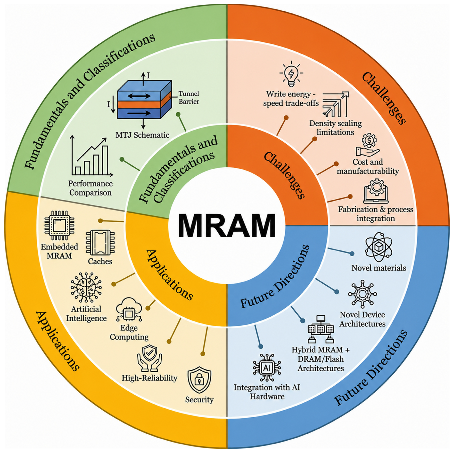
MRAM: A Versatile Non-Volatile Memory for Next-Generation Computing

Abstract
1. Introduction
2. Fundamentals and Evolution of MRAM
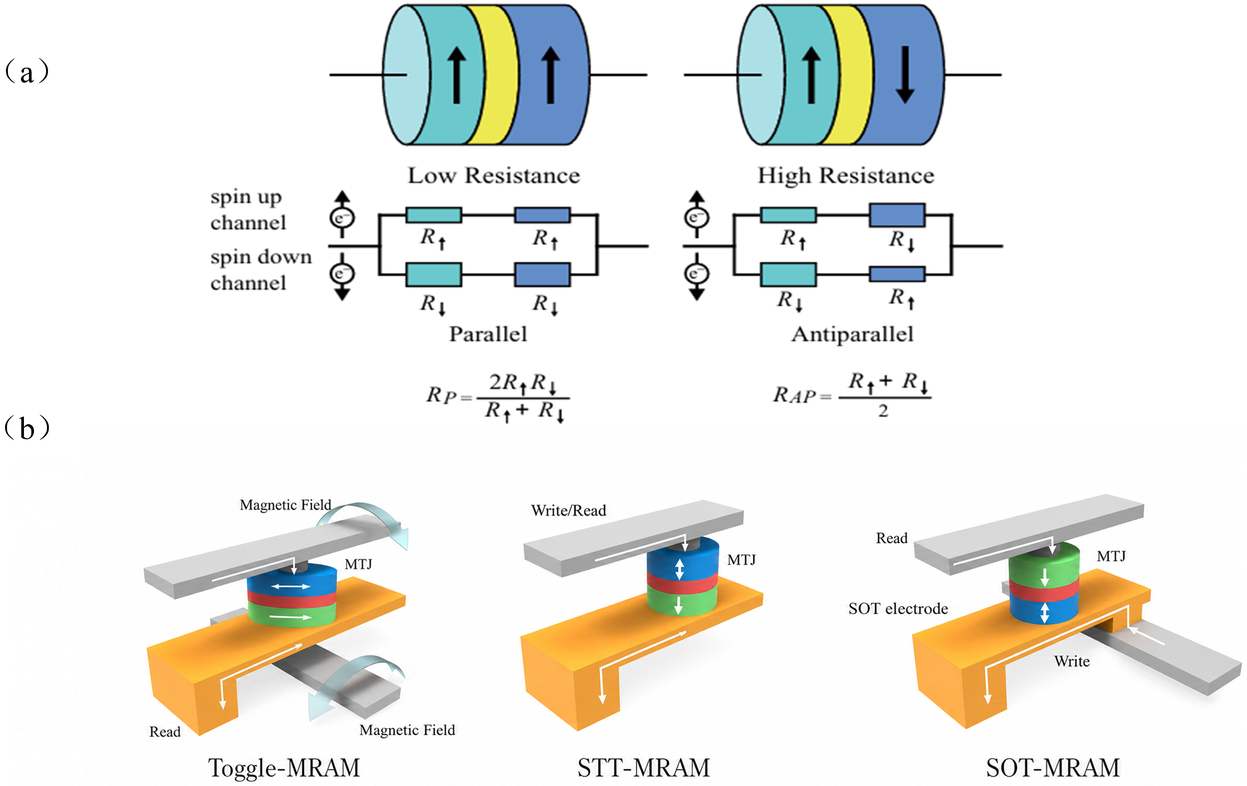
2.1. Fundamentals of MRAM

2.2. Evolution of MRAM
2.3. Performance Comparison
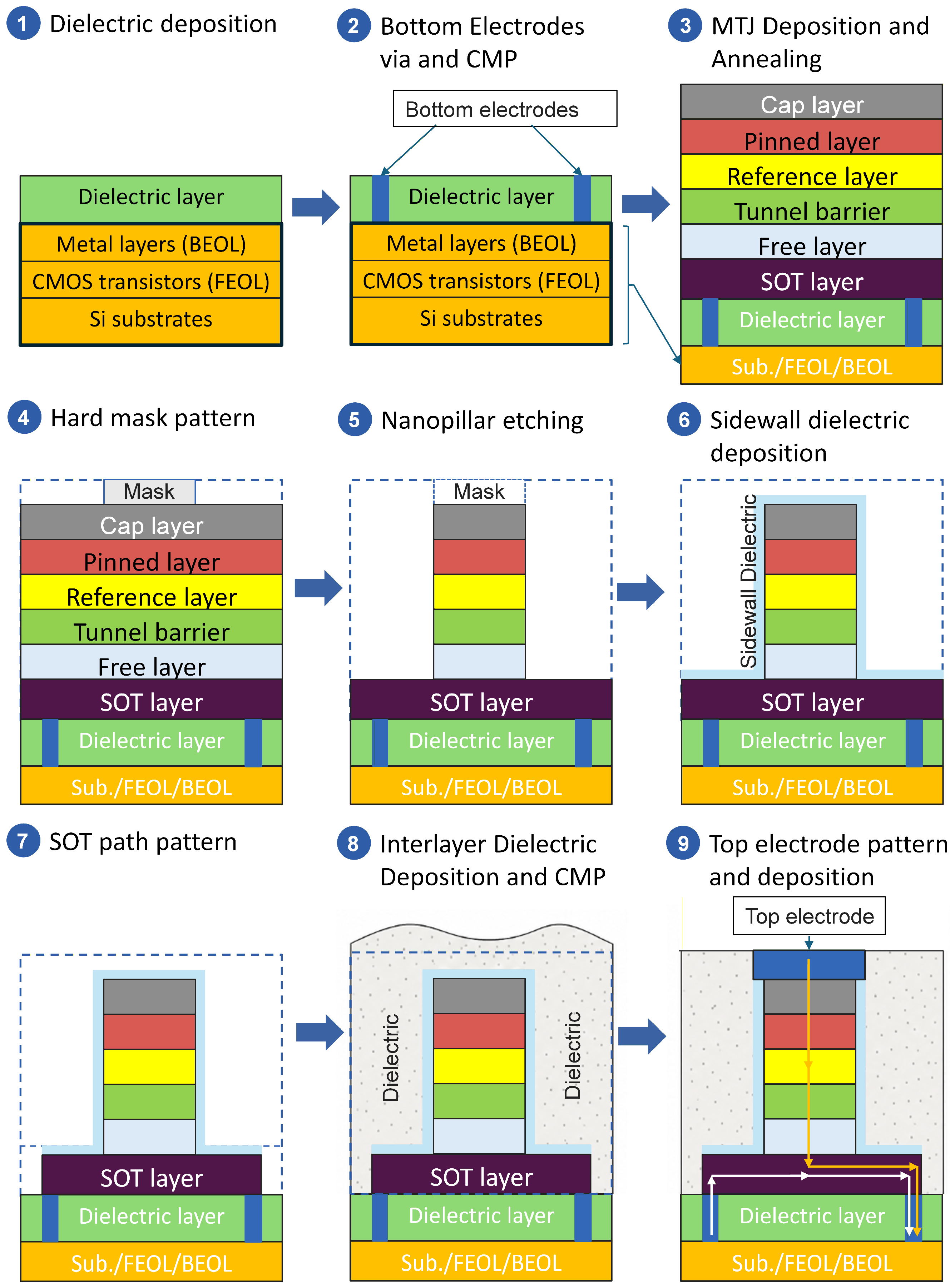
2.4. Fabrication Process of SOT-MRAM
- ①
- Dielectric deposition: After the conventional CMOS process is completed, a dielectric material (SiO2, SiNx) with an appropriate density and thickness is deposited on the Si substrate, where the CMOS transistors (including front-end-of-line (FEOL) devices) and BEOL metal interconnects have already been fabricated, thereby forming a dielectric layer to support the subsequent MTJ devices.
- ②
- Bottom electrode via and CMP: Bottom electrode via structures are formed by etching, enabling electrical connection between the bottom electrode and the underlying BEOL metal layer; metal is deposited to fill the vias and form the bottom electrode; then, chemical mechanical polishing (CMP) is performed to reduce the surface roughness (ideally below 0.2 nm), providing a flat and high-quality surface for the growth of the SOT-MTJ device, which is essential for ensuring the performance of SOT-MRAM.
- ③
- MTJ deposition and annealing: Since the SOT layer serves as the path for the write current to generate spin current that drives the magnetization switching of the free layer, SOT-MRAM adopts a top-pinned configuration, in which the pinned layer and reference layer are located near the top electrode, while the free layer is positioned adjacent to the SOT layer. The basic functional layer structure is illustrated in Figure 3③. A multilayer stack including the SOT layer, MTJ layers, and capping layer is deposited by magnetron sputtering. After stack deposition, vacuum annealing is usually performed under a magnetic field for better TMR values. During this step, current-in-plane tunneling (CIPT) measurement is required to monitor key properties of the film stack, such as the TMR ratio and RA.
- ④
- Hard mask pattern: A dielectric layer, normally SiO2, SiNx, or SiC, is deposited to serve as the hard mask later on. Then, photolithography is performed to define the hard mask pattern, then the hard mask layer is etched, followed by complete removal of the photoresist.
- ⑤
- MTJ nanopillar etching: The MTJ multilayer stack is etched and the hard mask is partially (the remaining part will be removed later on) or fully consumed during the etching. The etching process must be precisely stopped above the SOT channel layer, while ensuring that the free layer is completely etched.
- ⑥
- Sidewall dielectric deposition: An in situ sidewall dielectric layer is deposited to prevent moisture, oxygen, and other contaminants from degrading the MTJ layers.
- ⑦
- SOT layer pattern: Photolithography is performed to define the SOT channel pattern, and then to etch the SOT layer.
- ⑧
- Interlayer dielectric deposition and CMP: A dielectric layer is deposited to fill the gaps and isolate the MTJs, then CMP is first performed to planarize the surface.
- ⑨
- Top electrode pattern and deposition: An interlayer dielectric layer is deposited, photolithography is performed to define the top electrode via pattern above the MTJ; the dielectric layer is etched to form the top electrode via structure; then the top-electrode metal is deposited. Finally, the SOT-MRAM is ready, and the write current path is indicated by white arrows, whereas the read path is indicated by yellow arrows. Depending on the interconnection requirements, more than one metal layer may be formed after the MTJ. In addition, to meet the functional requirements of chip packaging, wire-bonding pads and a passivation layer need to be formed at the topmost level.
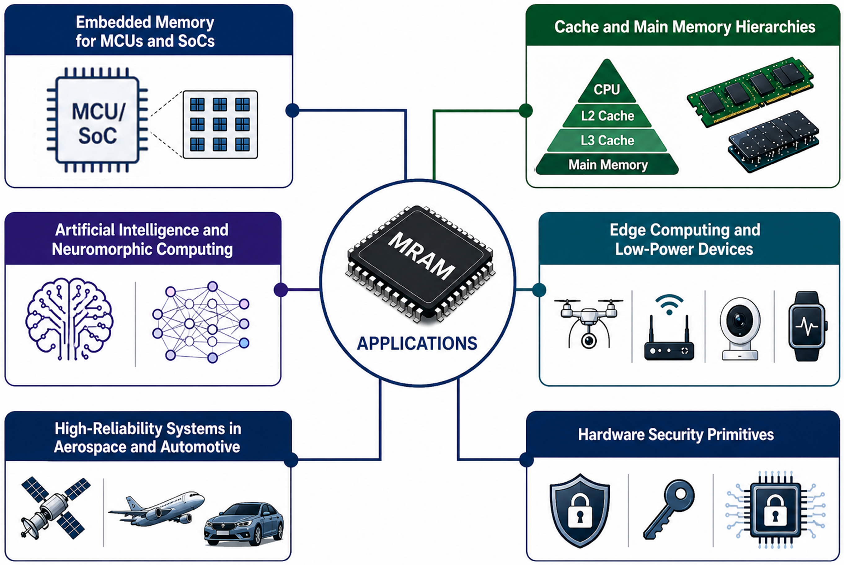
3. Applications of MRAM
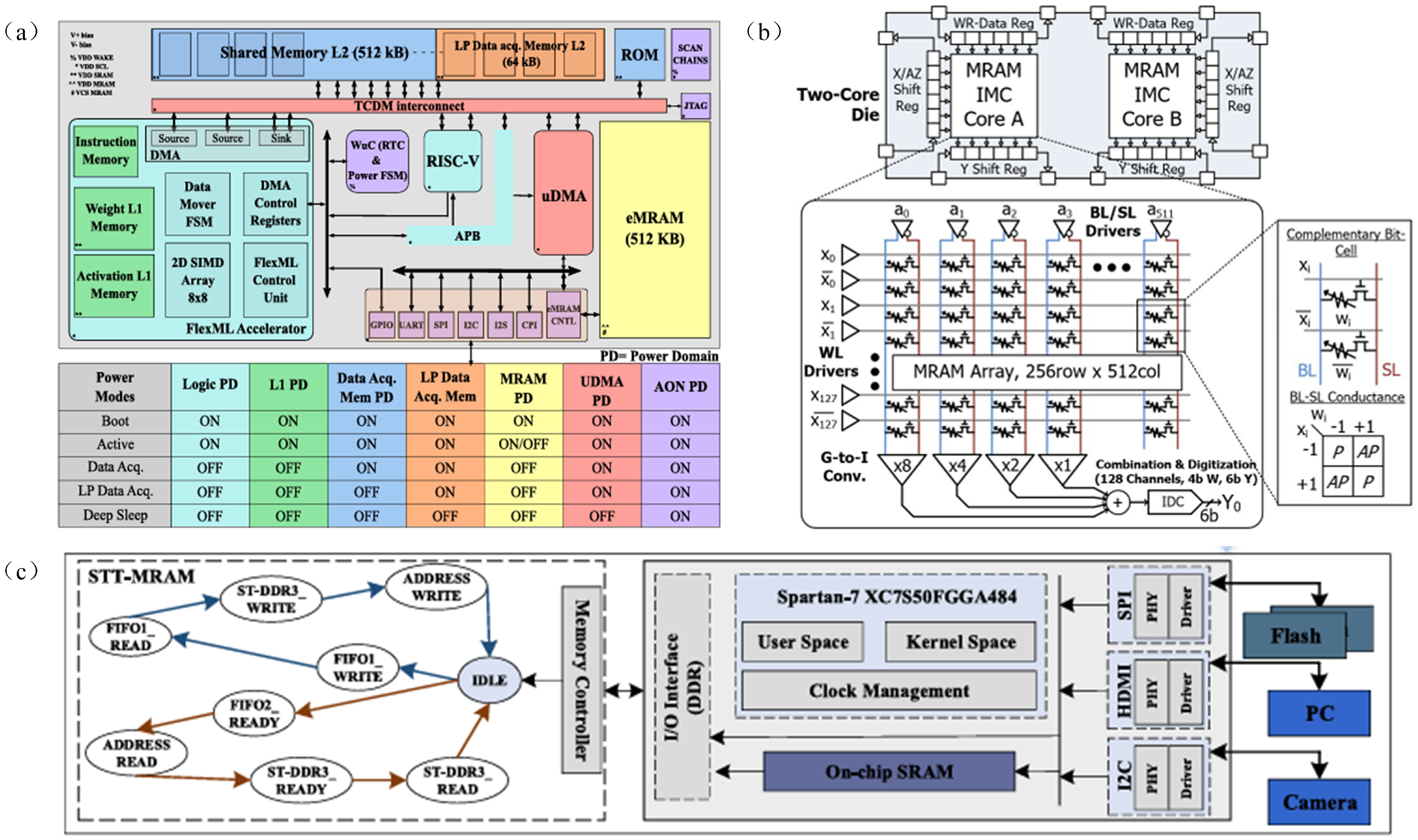
3.1. Embedded MRAM
3.2. MRAM in Caches and Main Memory
3.2.1. L2/L3 Cache Substitution
3.2.2. From Main Memory Integration to Near-Memory Storage
3.2.3. MRAM-Based Near-Memory Computing
3.3. MRAM in Artificial Intelligence
3.4. MRAM for Edge Computing and Wearables
3.5. MRAM in High-Reliability Domains
3.6. MRAM in Security Applications
4. Challenges
4.1. The Inherent Trade-Offs in Write Performance
4.2. Process Compatibility and Integration Complexity
4.3. Cost, Yield, and Commercialization Challenges
4.4. Physical and Architectural Limits to Density Scaling
5. Future Directions and Opportunities
5.1. Exploration of New Material
5.2. Novel Device Architectures
5.3. Integration with AI Hardware
5.4. In-Memory Computing
5.5. Hybrid Architectures
5.6. Commercialization Landscape and Ecosystem Growth
6. Conclusions
Author Contributions
Funding
Data Availability Statement
Conflicts of Interest
References
- McKee, S.A. Reflections on the Memory Wall. In Proceedings of the 1st Conference on Computing Frontiers; Association for Computing Machinery: New York, NY, USA, 2004; p. 162. [Google Scholar]
- Wulf, W.A.; McKee, S.A. Hitting the Memory Wall: Implications of the Obvious. SIGARCH Comput. Archit. News 1995, 23, 20–24. [Google Scholar] [CrossRef]
- Mittal, S.; Vetter, J.S.; Li, D. A Survey of Architectural Approaches for Managing Embedded DRAM and Non-Volatile On-Chip Caches. IEEE Trans. Parallel Distrib. Syst. 2015, 26, 1524–1537. [Google Scholar] [CrossRef]
- Grupp, L.M.; Davis, J.D.; Swanson, S. The Bleak Future of NAND Flash Memory. In Proceedings of the 10th USENIX Conference on File and Storage Technologies; USENIX Association: Berkeley, CA, USA, 2012; p. 2. [Google Scholar]
- Stuecheli, J.; Kaseridis, D.; Hunter, H.C.; John, L.K. Elastic Refresh: Techniques to Mitigate Refresh Penalties in High Density Memory. In Proceedings of the 2010 43rd Annual IEEE/ACM International Symposium on Microarchitecture; IEEE: New York, NY, USA, 2010; pp. 375–384. [Google Scholar]
- Nair, P.; Chou, C.-C.; Qureshi, M.K. A Case for Refresh Pausing in DRAM Memory Systems. In Proceedings of the 2013 IEEE 19th International Symposium on High Performance Computer Architecture (HPCA); IEEE: New York, NY, USA, 2013; pp. 627–638. [Google Scholar]
- Roy, K.; Mukhopadhyay, S.; Mahmoodi-Meimand, H. Leakage Current Mechanisms and Leakage Reduction Techniques in Deep-Submicrometer CMOS Circuits. Proc. IEEE 2003, 91, 305–327. [Google Scholar] [CrossRef]
- Daughton, J.M. Magnetoresistive Memory Technology. Thin Solid. Film. 1992, 216, 162–168. [Google Scholar] [CrossRef]
- Kent, A.D.; Worledge, D.C. A new spin on magnetic memories. Nat. Nanotechnol. 2015, 10, 187–191. [Google Scholar] [CrossRef] [PubMed]
- Nozaki, T.; Yamamoto, T.; Miwa, S.; Tsujikawa, M.; Shirai, M.; Yuasa, S.; Suzuki, Y. Recent Progress in the Voltage-Controlled Magnetic Anisotropy Effect and the Challenges Faced in Developing Voltage-Torque MRAM. Micromachines 2019, 10, 327. [Google Scholar] [CrossRef] [PubMed]
- Yuasa, S.; Nagahama, T.; Fukushima, A.; Suzuki, Y.; Ando, K. Giant Room-Temperature Magnetoresistance in Single-Crystal Fe/MgO/Fe Magnetic Tunnel Junctions. Nat. Mater. 2004, 3, 868–871. [Google Scholar] [CrossRef] [PubMed]
- Parkin, S.S.P.; Kaiser, C.; Panchula, A.; Rice, P.M.; Hughes, B.; Samant, M.; Yang, S.-H. Giant Tunnelling Magnetoresistance at Room Temperature with MgO (100) Tunnel Barriers. Nat. Mater. 2004, 3, 862–867. [Google Scholar] [CrossRef] [PubMed]
- Ikeda, S.; Hayakawa, J.; Ashizawa, Y.; Lee, Y.M.; Miura, K.; Hasegawa, H.; Tsunoda, M.; Matsukura, F.; Ohno, H. Tunnel Magnetoresistance of 604% at 300K by Suppression of Ta Diffusion in CoFeB/MgO/CoFeB Pseudo-Spin-Valves Annealed at High Temperature. Appl. Phys. Lett. 2008, 93, 082508. [Google Scholar] [CrossRef]
- Tsunekawa, K.; Djayaprawira, D.D.; Nagai, M.; Maehara, H.; Yamagata, S.; Watanabe, N.; Yuasa, S.; Suzuki, Y.; Ando, K. Giant Tunneling Magnetoresistance Effect in Low-Resistance CoFeB/MgO (001)/CoFeB Magnetic Tunnel Junctions for Read-Head Applications. Appl. Phys. Lett. 2005, 87, 072503. [Google Scholar] [CrossRef]
- Yakushiji, K.; Noma, K.; Saruya, T.; Kubota, H.; Fukushima, A.; Nagahama, T.; Yuasa, S.; Ando, K. High Magnetoresistance Ratio and Low Resistance–Area Product in Magnetic Tunnel Junctions with Perpendicularly Magnetized Electrodes. Appl. Phys. Express 2010, 3, 053003. [Google Scholar] [CrossRef]
- Wang, M.; Cai, W.; Cao, K.; Zhou, J.; Wrona, J.; Peng, S.; Yang, H.; Wei, J.; Kang, W.; Zhang, Y.; et al. Current-Induced Magnetization Switching in Atom-Thick Tungsten Engineered Perpendicular Magnetic Tunnel Junctions with Large Tunnel Magnetoresistance. Nat. Commun. 2018, 9, 671. [Google Scholar] [CrossRef] [PubMed]
- Tezuka, N.; Oikawa, S.; Abe, I.; Matsuura, M.; Sugimoto, S.; Nishimura, K.; Seino, T. Perpendicular Magnetic Tunnel Junctions With Low Resistance-Area Product: High Output Voltage and Bias Dependence of Magnetoresistance. IEEE Magn. Lett. 2016, 7, 3104204. [Google Scholar] [CrossRef]
- Peng, S.Z.; Zhang, Y.; Wang, M.X.; Zhang, Y.G.; Zhao, W. Magnetic Tunnel Junctions for Spintronics: Principles and Applications. In Wiley Encyclopedia of Electrical and Electronics Engineering; John Wiley & Sons: Hoboken, NJ, USA, 1999; pp. 1–16. [Google Scholar] [CrossRef]
- Guo, Z.; Yin, J.; Bai, Y.; Zhu, D.; Shi, K.; Wang, G.; Cao, K.; Zhao, W. Spintronics for Energy- Efficient Computing: An Overview and Outlook. Proc. IEEE 2021, 109, 1398–1417. [Google Scholar] [CrossRef]
- Slaughter, J.M. Materials for Magnetoresistive Random Access Memory. Annu. Rev. Mater. Res. 2009, 39, 277–296. [Google Scholar] [CrossRef]
- Zhang, L.; Zhou, J.; Li, H.; Shen, L.; Feng, Y.P. Recent Progress and Challenges in Magnetic Tunnel Junctions with 2D Materials for Spintronic Applications. Appl. Phys. Rev. 2021, 8, 021308. [Google Scholar] [CrossRef]
- Apalkov, D.; Dieny, B.; Slaughter, J.M. Magnetoresistive Random Access Memory. Proc. IEEE 2016, 104, 1796–1830. [Google Scholar] [CrossRef]
- Ikegawa, S.; Mancoff, F.B.; Janesky, J.; Aggarwal, S. Magnetoresistive Random Access Memory: Present and Future. IEEE Trans. Electron. Devices 2020, 67, 1407–1419. [Google Scholar] [CrossRef]
- Butler, W.H.; Zhang, X.-G.; Schulthess, T.C.; MacLaren, J.M. Spin-dependent tunneling conductance of Fe| MgO| Fe sandwiches. Phys. Rev. B 2001, 63, 054416. [Google Scholar] [CrossRef]
- Mathon, J.; Umerski, A. Theory of tunneling magnetoresistance of an epitaxial Fe/MgO/Fe (001) junction. Phys. Rev. B 2001, 63, 220403. [Google Scholar] [CrossRef]
- Berger, L. Emission of spin waves by a magnetic multilayer traversed by a current. Phys. Rev. B 1996, 54, 9353–9358. [Google Scholar] [CrossRef] [PubMed]
- Moodera, J.S.; Kinder, L.R.; Wong, T.M.; Meservey, R. Large magnetoresistance at room temperature in ferromagnetic thin film tunnel junctions. Phys. Rev. Lett. 1995, 74, 3273–3276. [Google Scholar] [CrossRef] [PubMed]
- Engel, B.N.; Akerman, J.; Butcher, B.; Dave, R.W.; DeHerrera, M.; Durlam, M.; Grynkewich, G.; Janesky, J.; Pietambaram, S.V.; Rizzo, N.D.; et al. A 4-Mb toggle MRAM based on a novel bit and switching method. IEEE Trans. Magn. 2005, 41, 132–136. [Google Scholar] [CrossRef]
- Yuasa, S.; Hono, K.; Hu, G.; Worledge, D.C. Materials for Spin-Transfer-Torque Magnetoresistive Random-Access Memory. MRS Bull. 2018, 43, 352–357. [Google Scholar] [CrossRef]
- Dieny, B.; Chshiev, M. Perpendicular Magnetic Anisotropy at Transition Metal/Oxide Interfaces and Applications. Rev. Mod. Phys. 2017, 89, 025008. [Google Scholar] [CrossRef]
- Sbiaa, R.; Meng, H.; Piramanayagam, S.N. Materials with Perpendicular Magnetic Anisotropy for Magnetic Random Access Memory. Phys. Status Solidi RRL 2011, 5, 413–419. [Google Scholar] [CrossRef]
- Worledge, D.C.; Hu, G. Spin-Transfer Torque Magnetoresistive Random Access Memory Technology Status and Future Directions. Nat. Rev. Electr. Eng. 2024, 1, 730–747. [Google Scholar] [CrossRef]
- Bhatti, S.; Sbiaa, R.; Hirohata, A.; Ohno, H.; Fukami, S.; Piramanayagam, S.N. Spintronics based random access memory: A review. Mater. Today 2017, 20, 530–554. [Google Scholar] [CrossRef]
- Lee, K.; Bak, J.H.; Kim, Y.J.; Kim, C.K.; Antonyan, A.; Chang, D.H.; Hwang, S.H.; Lee, G.W.; Ji, N.Y.; Kim, W.J.; et al. 1Gbit High Density Embedded STT-MRAM in 28nm FDSOI Technology. In Proceedings of the 2019 IEEE International Electron Devices Meeting (IEDM); IEEE: New York, NY, USA, 2019; pp. 2.2.1–2.2.4. [Google Scholar]
- Lee, T.Y.; Lee, J.M.; Kim, M.K.; Oh, J.S.; Lee, J.W.; Jeong, H.M.; Jang, P.H.; Joo, M.K.; Suh, K.; Han, S.H.; et al. World-Most Energy-Efficient MRAM Technology for Non-Volatile RAM Applications. In Proceedings of the 2022 International Electron Devices Meeting (IEDM); IEEE: New York, NY, USA, 2022; pp. 10.7.1–10.7.4. [Google Scholar]
- Everspin Launches a New Family of SPI Interface MRAM Products|MRAM-Info. Available online: https://www.mram-info.com/everspin-launches-new-family-spi-interface-mram-products (accessed on 5 May 2026).
- Miron, I.M.; Garello, K.; Gaudin, G.; Zermatten, P.-J.; Costache, M.V.; Auffret, S.; Bandiera, S.; Rodmacq, B.; Schuhl, A.; Gambardella, P. Perpendicular Switching of a Single Ferromagnetic Layer Induced by In-Plane Current Injection. Nature 2011, 476, 189–193. [Google Scholar] [CrossRef] [PubMed]
- Liu, L.; Lee, O.J.; Gudmundsen, T.J.; Ralph, D.C.; Buhrman, R.A. Current-Induced Switching of Perpendicularly Magnetized Magnetic Layers Using Spin Torque from the Spin Hall Effect. Phys. Rev. Lett. 2012, 109, 096602. [Google Scholar] [CrossRef] [PubMed]
- Liu, L.; Pai, C.-F.; Li, Y.; Tseng, H.W.; Ralph, D.C.; Buhrman, R.A. Spin-Torque Switching with the Giant Spin Hall Effect of Tantalum. Science 2012, 336, 555–558. [Google Scholar] [CrossRef] [PubMed]
- Pai, C.-F.; Liu, L.; Li, Y.; Tseng, H.W.; Ralph, D.C.; Buhrman, R.A. Spin Transfer Torque Devices Utilizing the Giant Spin Hall Effect of Tungsten. Appl. Phys. Lett. 2012, 101, 122404. [Google Scholar] [CrossRef]
- Kim, J.Y.; Oh, K.H.; Kim, G.W.; Baek, S.C.; Lee, D.; Lee, K.D.; Park, B.G. Enhancement of Spin Hall Conductivity in W–Ta Alloy. Appl. Phys. Lett. 2020, 117, 142403. [Google Scholar] [CrossRef]
- Kim, J.; Sinha, J.; Hayashi, M.; Yamanouchi, M.; Fukami, S.; Suzuki, T.; Mitani, S.; Ohno, H. Layer Thickness Dependence of the Current-Induced Effective Field Vector in Ta|CoFeB|MgO. Nat. Mater. 2013, 12, 240–245. [Google Scholar] [CrossRef] [PubMed]
- Krizakova, V.; Perumkunnil, M.; Couet, S.; Gambardella, P.; Garello, K. Spin-Orbit Torque Switching of Magnetic Tunnel Junctions for Memory Applications. J. Magn. Magn. Mater. 2022, 562, 169692. [Google Scholar] [CrossRef]
- Garello, K.; Miron, I.M.; Avci, C.O.; Freimuth, F.; Mokrousov, Y.; Blügel, S.; Auffret, S.; Boulle, O.; Gaudin, G.; Gambardella, P. Symmetry and Magnitude of Spin–Orbit Torques in Ferromagnetic Heterostructures. Nat. Nanotechnol. 2013, 8, 587–593. [Google Scholar] [CrossRef] [PubMed]
- Hu, C.-Y.; Chen, W.-D.; Liu, Y.-T.; Huang, C.-C.; Pai, C.-F. The Central Role of Tilted Anisotropy for Field-Free Spin–Orbit Torque Switching of Perpendicular Magnetization. NPG Asia Mater. 2024, 16, 1. [Google Scholar] [CrossRef]
- Xue, F.; Lin, S.-J.; Song, M.; Hwang, W.; Klewe, C.; Lee, C.-M.; Turgut, E.; Shafer, P.; Vailionis, A.; Huang, Y.-L.; et al. Field-Free Spin-Orbit Torque Switching Assisted by In-Plane Unconventional Spin Torque in Ultrathin [Pt/Co]N. Nat. Commun. 2023, 14, 3932. [Google Scholar] [CrossRef] [PubMed]
- Pandey, L.; Zhao, B.; Tenzin, K.; Ngaloy, R.; Lamparská, V.; Bangar, H.; Ali, A.; Abdel-Hafiez, M.; Zhang, G.; Wu, H.; et al. Tunable Unconventional Spin Orbit Torque Magnetization Dynamics in van der Waals Heterostructures. Nat. Commun. 2025, 16, 8722. [Google Scholar] [CrossRef] [PubMed]
- Kang, M.-G.; Lee, S.; Park, B.-G. Field-Free Spin-Orbit Torques Switching and Its Applications. npj Spintron. 2025, 3, 8. [Google Scholar] [CrossRef]
- Wang, M.; Cai, W.; Zhu, D.; Wang, Z.; Kan, J.; Zhao, Z.; Cao, K.; Wang, Z.; Zhang, Y.; Zhang, T.; et al. Field-Free Switching of a Perpendicular Magnetic Tunnel Junction through the Interplay of Spin–Orbit and Spin-Transfer Torques. Nat. Electron. 2018, 1, 582–588. [Google Scholar] [CrossRef]
- Zhang, H.; Ma, X.; Jiang, C.; Yin, J.; Lyu, S.; Lu, S.; Shang, X.; Man, B.; Zhang, C.; Li, D.; et al. Integration of High-Performance Spin-Orbit Torque MRAM Devices by 200-Mm-Wafer Manufacturing Platform. J. Semicond. 2022, 43, 102501–102509. [Google Scholar] [CrossRef]
- Jiang, C.; Li, J.; Zhang, H.; Lu, S.; Li, P.; Wang, C.; Zhang, Z.; Hou, Z.; Liu, X.; Feng, J.; et al. Demonstration of a Manufacturable SOT-MRAM Multiplexer Array towards Industrial Applications. J. Semicond. 2023, 44, 122501. [Google Scholar] [CrossRef]
- Huang, Y.-L.; Song, M.; Lee, C.-M.; Chen, Y.-W.; Chiang, C.-Y.; Chou, S.-H.; Hsu, L.-C.; Liu, H.-J.; Chen, G.-L.; Yang, S.-Y.; et al. A 64-Kilobit Spin–Orbit Torque Magnetic Random-Access Memory Based on Back-End-of-Line-Compatible β-Tungsten. Nat. Electron. 2025, 8, 794–802. [Google Scholar] [CrossRef]
- Apalkov, D.; Khvalkovskiy, A.; Watts, S.; Nikitin, V.; Tang, X.; Lottis, D.; Moon, K.; Luo, X.; Chen, E.; Ong, A.; et al. Spin-Transfer Torque Magnetic Random Access Memory (STT-MRAM). J. Emerg. Technol. Comput. Syst. 2013, 9, 1–35. [Google Scholar] [CrossRef]
- Durlam, M.; Addie, D.; Akerman, J.; Butcher, B.; Brown, P.; Chan, J.; DeHerrera, M.; Engel, B.N.; Feil, B.; Grynkewich, G.; et al. A 0.18/Spl Mu/m 4 Mbit Toggling MRAM. In Proceedings of the 2004 International Conference on Integrated Circuit Design and Technology; IEEE: New York, NY, USA, 2004; pp. 27–30. [Google Scholar]
- Beach, R.; Min, T.; Horng, C.; Chen, Q.; Sherman, P.; Le, S.; Young, S.; Yang, K.; Yu, H.; Lu, X.; et al. A Statistical Study of Magnetic Tunnel Junctions for High-Density Spin Torque Transfer-MRAM (STT-MRAM). In Proceedings of the 2008 IEEE International Electron Devices Meeting; IEEE: New York, NY, USA, 2008; pp. 1–4. [Google Scholar]
- Nebashi, R.; Sakimura, N.; Honjo, H.; Saito, S.; Ito, Y.; Miura, S.; Kato, Y.; Mori, K.; Ozaki, Y.; Kobayashi, Y.; et al. A 90nm 12ns 32Mb 2T1MTJ MRAM. In Proceedings of the 2009 IEEE International Solid-State Circuits Conference—Digest of Technical Papers; IEEE: New York, NY, USA, 2009; pp. 462–463,463a. [Google Scholar]
- Halupka, D.; Huda, S.; Song, W.; Sheikholeslami, A.; Tsunoda, K.; Yoshida, C.; Aoki, M. Negative-Resistance Read and Write Schemes for STT-MRAM in 0.13 µm CMOS. In Proceedings of the 2010 IEEE International Solid-State Circuits Conference—(ISSCC); IEEE: New York, NY, USA, 2010; pp. 256–257. [Google Scholar]
- Tsuchida, K.; Inaba, T.; Fujita, K.; Ueda, Y.; Shimizu, T.; Asao, Y.; Kajiyama, T.; Iwayama, M.; Sugiura, K.; Ikegawa, S.; et al. A 64Mb MRAM with Clamped-Reference and Adequate-Reference Schemes. In Proceedings of the 2010 IEEE International Solid-State Circuits Conference—(ISSCC); IEEE: New York, NY, USA, 2010; pp. 258–259. [Google Scholar]
- Chung, S.; Rho, K.-M.; Kim, S.-D.; Suh, H.-J.; Kim, D.-J.; Kim, H.-J.; Lee, S.-H.; Park, J.-H.; Hwang, H.-M.; Hwang, S.-M.; et al. Fully Integrated 54nm STT-RAM with the Smallest Bit Cell Dimension for High Density Memory Application. In Proceedings of the 2010 International Electron Devices Meeting; IEEE: New York, NY, USA, 2010; pp. 12.7.1–12.7.4. [Google Scholar]
- Takemura, R.; Kawahara, T.; Miura, K.; Yamamoto, H.; Hayakawa, J.; Matsuzaki, N.; Ono, K.; Yamanouchi, M.; Ito, K.; Takahashi, H.; et al. A 32-Mb SPRAM With 2T1R Memory Cell, Localized Bi-Directional Write Driver and ‘1’/‘0’ Dual-Array Equalized Reference Scheme. IEEE J. Solid-State Circuits 2010, 45, 869–879. [Google Scholar] [CrossRef]
- Worledge, D.C.; Hu, G.; Trouilloud, P.L.; Abraham, D.W.; Brown, S.; Gaidis, M.C.; Nowak, J.; O’Sullivan, E.J.; Robertazzi, R.P.; Sun, J.Z.; et al. Switching Distributions and Write Reliability of Perpendicular Spin Torque MRAM. In Proceedings of the 2010 International Electron Devices Meeting; IEEE: New York, NY, USA, 2010; pp. 12.5.1–12.5.4. [Google Scholar]
- Kim, J.P.; Kim, T.; Hao, W.; Rao, H.M.; Lee, K.; Zhu, X.; Li, X.; Hsu, W.; Kang, S.H.; Matt, N.; et al. A 45nm 1Mb Embedded STT-MRAM with Design Techniques to Minimize Read-Disturbance. In Proceedings of the 2011 Symposium on VLSI Circuits—Digest of Technical Papers; IEEE: New York, NY, USA, 2011; pp. 296–297. [Google Scholar]
- Slaughter, J.M.; Rizzo, N.D.; Janesky, J.; Whig, R.; Mancoff, F.B.; Houssameddine, D.; Sun, J.J.; Aggarwal, S.; Nagel, K.; Deshpande, S.; et al. High Density ST-MRAM Technology (Invited). In Proceedings of the 2012 International Electron Devices Meeting; IEEE: New York, NY, USA, 2012; pp. 29.3.1–29.3.4. [Google Scholar]
- Yu, H.-C.; Lin, K.-C.; Lin, K.-F.; Huang, C.-Y.; Chih, Y.-D.; Ong, T.-C.; Chang, J.; Natarajan, S.; Tran, L.C. Cycling Endurance Optimization Scheme for 1Mb STT-MRAM in 40nm Technology. In Proceedings of the 2013 IEEE International Solid-State Circuits Conference Digest of Technical Papers; IEEE: New York, NY, USA, 2013; pp. 224–225. [Google Scholar]
- Ohsawa, T.; Miura, S.; Kinoshita, K.; Honjo, H.; Ikeda, S.; Hanyu, T.; Ohno, H.; Endoh, T. A 1.5nsec/2.1nsec Random Read/Write Cycle 1Mb STT-RAM Using 6T2MTJ Cell with Background Write for Nonvolatile e-Memories. In Proceedings of the 2013 Symposium on VLSI Circuits; IEEE: New York, NY, USA, 2013; pp. C110–C111. [Google Scholar]
- Lee, Y.J.; Jan, G.; Wang, Y.J.; Pi, K.; Zhong, T.; Tong, R.Y.; Lam, V.; Teng, J.; Huang, K.; He, R.R.; et al. Demonstration of Chip Level Writability, Endurance and Data Retention of an Entire 8Mb STT-MRAM Array. In Proceedings of the 2013 International Symposium on VLSI Technology, Systems and Application (VLSI-TSA); IEEE: New York, NY, USA, 2013; pp. 1–2. [Google Scholar]
- Kawasumi, A.; Kushida, K.; Hara, H.; Unekawa, Y.; Abe, K.; Ikegami, K.; Noguchi, H.; Kitagawa, E.; Kamata, C.; Kashiwada, S.; et al. Circuit Techniques in Realizing Voltage-Generator-Less STT MRAM Suitable for Normally-off-Type Non-Volatile L2 Cache Memory. In Proceedings of the 2013 5th IEEE International Memory Workshop; IEEE: New York, NY, USA, 2013; pp. 76–79. [Google Scholar]
- Noguchi, H.; Kushida, K.; Ikegami, K.; Abe, K.; Kitagawa, E.; Kashiwada, S.; Kamata, C.; Kawasumi, A.; Hara, H.; Fujita, S. A 250-MHz 256b-I/O 1-Mb STT-MRAM with Advanced Perpendicular MTJ Based Dual Cell for Nonvolatile Magnetic Caches to Reduce Active Power of Processors. In Proceedings of the 2013 Symposium on VLSI Technology; IEEE: New York, NY, USA, 2013; pp. C108–C109. [Google Scholar]
- Jan, G.; Thomas, L.; Le, S.; Lee, Y.-J.; Liu, H.; Zhu, J.; Tong, R.-Y.; Pi, K.; Wang, Y.-J.; Shen, D.; et al. Demonstration of Fully Functional 8Mb Perpendicular STT-MRAM Chips with Sub-5ns Writing for Non-Volatile Embedded Memories. In Proceedings of the 2014 Symposium on VLSI Technology (VLSI-Technology): Digest of Technical Papers; IEEE: New York, NY, USA, 2014; pp. 1–2. [Google Scholar]
- DeBrosse, J.; Maffitt, T.; Nakamura, Y.; Jan, G.; Wang, P.-K. A Fully-Functional 90nm 8Mb STT MRAM Demonstrator Featuring Trimmed, Reference Cell-Based Sensing. In Proceedings of the 2015 IEEE Custom Integrated Circuits Conference (CICC); IEEE: New York, NY, USA, 2015; pp. 1–3. [Google Scholar]
- Noguchi, H.; Ikegami, K.; Kushida, K.; Abe, K.; Itai, S.; Takaya, S.; Shimomura, N.; Ito, J.; Kawasumi, A.; Hara, H.; et al. 7.5 A 3.3ns-Access-Time 71.2μW/MHz 1Mb Embedded STT-MRAM Using Physically Eliminated Read-Disturb Scheme and Normally-off Memory Architecture. In Proceedings of the 2015 IEEE International Solid-State Circuits Conference—(ISSCC) Digest of Technical Papers; IEEE: New York, NY, USA, 2015; pp. 1–3. [Google Scholar]
- Noguchi, H.; Ikegami, K.; Takaya, S.; Arima, E.; Kushida, K.; Kawasumi, A.; Hara, H.; Abe, K.; Shimomura, N.; Ito, J.; et al. 7.2 4Mb STT-MRAM-Based Cache with Memory-Access-Aware Power Optimization and Write-Verify-Write/Read-Modify-Write Scheme. In Proceedings of the 2016 IEEE International Solid-State Circuits Conference (ISSCC); IEEE: New York, NY, USA, 2016; pp. 132–133. [Google Scholar]
- Antonyan, A.; Pyo, S.; Jung, H.; Koh, G.-H.; Song, T. 28-Nm 1T-1MTJ 8Mb 64 I/O STT-MRAM with Symmetric 3-Section Reference Structure and Cross-Coupled Sensing Amplifier. In Proceedings of the 2017 IEEE International Symposium on Circuits and Systems (ISCAS); IEEE: New York, NY, USA, 2017; pp. 1–4. [Google Scholar]
- Dong, Q.; Wang, Z.; Lim, J.; Zhang, Y.; Shih, Y.-C.; Chih, Y.-D.; Chang, J.; Blaauw, D.; Sylvester, D. A 1Mb 28nm STT-MRAM with 2.8ns Read Access Time at 1.2V VDD Using Single-Cap Offset-Cancelled Sense Amplifier and in-Situ Self-Write-Termination. In Proceedings of the 2018 IEEE International Solid-State Circuits Conference—(ISSCC); IEEE: New York, NY, USA, 2018; pp. 480–482. [Google Scholar]
- Aggarwal, S.; Almasi, H.; DeHerrera, M.; Hughes, B.; Ikegawa, S.; Janesky, J.; Lee, H.K.; Lu, H.; Mancoff, F.B.; Nagel, K.; et al. Demonstration of a Reliable 1 Gb Standalone Spin-Transfer Torque MRAM For Industrial Applications. In Proceedings of the 2019 IEEE International Electron Devices Meeting (IEDM); IEEE: New York, NY, USA, 2019; pp. 2.1.1–2.1.4. [Google Scholar]
- Alzate, J.G.; Arslan, U.; Bai, P.; Brockman, J.; Chen, Y.J.; Das, N.; Fischer, K.; Ghani, T.; Heil, P.; Hentges, P.; et al. 2 MB Array-Level Demonstration of STT-MRAM Process and Performance Towards L4 Cache Applications. In Proceedings of the 2019 IEEE International Electron Devices Meeting (IEDM); IEEE: New York, NY, USA, 2019; pp. 2.4.1–2.4.4. [Google Scholar]
- Edwards, E.R.J.; Hu, G.; Brown, S.L.; D’Emic, C.P.; Gottwald, M.G.; Hashemi, P.; Jung, H.; Kim, J.; Lauer, G.; Nowak, J.J.; et al. Demonstration of Narrow Switching Distributions in STTMRAM Arrays for LLC Applications at 1x Nm Node. In Proceedings I have checked and revised allof the 2020 IEEE International Electron Devices Meeting (IEDM); IEEE: New York, NY, USA, 2020; pp. 24.4.1–24.4.4. [Google Scholar]
- Boujamaa, E.M.; Ali, S.M.; Wandji, S.N.; Gourio, A.; Pyo, S.; Koh, G.; Song, Y.; Song, T.; Kye, J.; Vial, J.C.; et al. A 14.7Mb/Mm2 28nm FDSOI STT-MRAM with Current Starved Read Path, 52Ω/Sigma Offset Voltage Sense Amplifier and Fully Trimmable CTAT Reference. In Proceedings of the 2020 IEEE Symposium on VLSI Circuits; IEEE: New York, NY, USA, 2020; pp. 1–2. [Google Scholar]
- Ogawa, T.; Matsubara, K.; Taito, Y.; Saito, T.; Izuna, M.; Takeda, K.; Kaneda, Y.; Shimoi, T.; Mitani, H.; Ito, T.; et al. 15.8 A 22nm 10.8Mb Embedded STT-MRAM Macro Achieving over 200MHz Random-Read Access and a 10.4MB/s Write Throughput with an In-Field Programmable 0.3Mb MTJ-OTP for High-End MCUs. In Proceedings of the 2024 IEEE International Solid-State Circuits Conference (ISSCC); IEEE: New York, NY, USA, 2024; Volume 67, pp. 290–292. [Google Scholar]
- Khvalkovskiy, A.V.; Apalkov, D.; Watts, S.; Chepulskii, R.; Beach, R.S.; Ong, A.; Tang, X.; Driskill-Smith, A.; Butler, W.H.; Visscher, P.B.; et al. Basic Principles of STT-MRAM Cell Operation in Memory Arrays. J. Phys. D Appl. Phys. 2013, 46, 074001. [Google Scholar] [CrossRef]
- Micheloni, R.; Aritome, S.; Crippa, L. Array Architectures for 3-D NAND Flash Memories. Proc. IEEE 2017, 105, 1634–1649. [Google Scholar] [CrossRef]
- Hsu, T.-H.; Lue, H.-T.; Hsu, P.-K.; Yeh, T.-H.; Du, P.-Y.; Lee, G.-R.; Chiu, C.-J.; Wang, K.-C.; Lu, C.-Y. A Vertical Split-Gate Flash Memory Featuring High-Speed Source-Side Injection Programming, Read Disturb Free, and 100K Endurance for Embedded Flash (eFlash) Scaling and Computing-In-Memory (CIM). In Proceedings of the 2020 IEEE International Electron Devices Meeting (IEDM); IEEE: New York, NY, USA, 2020; pp. 6.3.1–6.3.4. [Google Scholar]
- Horowitz, M. 1.1 Computing’s Energy Problem (and What We Can Do about It). In 2014 IEEE International Solid-State Circuits Conference Digest of Technical Papers (ISSCC); IEEE: San Francisco, CA, USA, 2014; pp. 10–14. [Google Scholar]
- Hoefflinger, B. ITRS: The International Technology Roadmap for Semiconductors. In Chips 2020: A Guide to the Future of Nanoelectronics; Hoefflinger, B., Ed.; Springer: Berlin/Heidelberg, Germany, 2012; pp. 161–174. [Google Scholar]
- Antonyan, A.; Pyo, S.; Jung, H.; Song, T. Embedded MRAM Macro for eFlash Replacement. In Proceedings of the 2018 IEEE International Symposium on Circuits and Systems (ISCAS); IEEE: New York, NY, USA, 2018; pp. 1–4. [Google Scholar]
- Müller, J.; Pfefferling, B.; Merbeth, T.; Otani, Y.; Hazen, D.S.; Hula, T.; Mansueto, M.; Titova, A.; Ramasubramanian, L.; Grimm, C.V.-B.; et al. Embedded STT-MRAM for Automotive Applications. In Proceedings of the 2024 8th IEEE Electron Devices Technology & Manufacturing Conference (EDTM); IEEE: New York, NY, USA, 2024; pp. 1–3. [Google Scholar]
- Lee, Y.K.; Song, Y.; Kim, J.; Oh, S.; Bae, B.-J.; Lee, S.; Lee, J.; Pi, U.; Seo, B.; Jung, H.; et al. Embedded STT-MRAM in 28-Nm FDSOI Logic Process for Industrial MCU/IoT Application. In Proceedings of the 2018 IEEE Symposium on VLSI Technology; IEEE: New York, NY, USA, 2018; pp. 181–182. [Google Scholar]
- Lee, D.; Fong, X.; Roy, K. R-MRAM: A ROM-Embedded STT MRAM Cache. IEEE Electron. Device Lett. 2013, 34, 1256–1258. [Google Scholar] [CrossRef]
- Shimoi, T.; Matsubara, K.; Saito, T.; Ogawa, T.; Taito, Y.; Kaneda, Y.; Izuna, M.; Takeda, K.; Mitani, H.; Ito, T.; et al. A 22-Nm 32-Mb Embedded STT-MRAM Macro Achieving 5.9-Ns Random Read Access and 7.4-MB/s Write Throughput at up to 150 °C. IEEE J. Solid-State Circuits 2024, 59, 1283–1292. [Google Scholar] [CrossRef]
- Jain, V.; Giraldo, S.; Roose, J.D.; Mei, L.; Boons, B.; Verhelst, M. TinyVers: A Tiny Versatile System-on-Chip With State-Retentive eMRAM for ML Inference at the Extreme Edge. IEEE J. Solid-State Circuits 2023, 58, 2360–2371. [Google Scholar] [CrossRef]
- Myung, S.; Yun, S.-J.; Kim, M.; Yi, W.; Lee, J.; An, J.; Lee, K.-R.; Shin, C.-W.; Jung, S.; Kwon, S. A 14 Nm MRAM-Based Multi-Bit Analog In-Memory Computing With Process-Variation Calibration for 72 Macros-Based Accelerator. IEEE J. Solid-State Circuits 2024, 7, 295–298. [Google Scholar] [CrossRef]
- Deaville, P.; Zhang, B.; Verma, N. A Fully Row/Column-Parallel In-Memory Computing Macro in Foundry MRAM with Differential Readout for Noise Rejection. IEEE J. Solid-State Circuits 2024, 59, 2070–2080. [Google Scholar] [CrossRef]
- Qi, L.; Fan, J.; Cai, H.; Fang, Z. A Survey of Emerging Memory in a Microcontroller Unit. Micromachines 2024, 15, 488. [Google Scholar] [CrossRef] [PubMed]
- Lee, Y.-J.; Cheng, C.-T.; Huang, J.-C.; Huang, K.-F.; Lin, B.-H.; Lin, B.; Tseng, K.C.; Jinnai, B.; Tsai, M.-H.; Jiang, M.-R.; et al. Demonstration of Embedded MRAM with Sub-50 Nm MTJ for RAM-Like and MCU Applications. In Proceedings of the 2025 Symposium on VLSI Technology and Circuits (VLSI Technology and Circuits); IEEE: New York, NY, USA, 2025; pp. 1–3. [Google Scholar]
- Lee, T.Y.; Lee, J.M.; Oh, Y.W.; Kim, H.-H.; Kwon, B.S.; Yamane, K.; Kim, M.K.; Jang, P.H.; Lee, D.K.; Gwak, H.J.; et al. World-Most Energy-Efficient 14nm Automotive eMRAM Technology for High-Endurance Applications. In Proceedings of the 2024 IEEE International Electron Devices Meeting (IEDM); IEEE: New York, NY, USA, 2024; pp. 1–4. [Google Scholar]
- Li, Y.; Kang, W.; Zhou, K.; Qiu, K.; Zhao, W. Experimental Demonstration of STT-MRAM-Based Nonvolatile Instantly On/Off System for IoT Applications: Case Studies. ACM Trans. Embed. Comput. Syst. 2023, 22, 1–24. [Google Scholar] [CrossRef]
- Sun, B.; Liu, D.; Yu, L.; Li, J.; Liu, H.; Zhang, W.; Torng, T. MRAM Co-Designed Processing-in-Memory CNN Accelerator for Mobile and IoT Applications. arXiv 2018, arXiv:1811.12179, 2018. [Google Scholar]
- Zhang, Z.; Wang, W.; Yu, P.; Jiang Member, I. Yanfeng Cache Performance of NV-STT-MRAM with Scale Effect and Comparison with SRAM. Int. J. Electron. 2022, 109, 391–409. [Google Scholar] [CrossRef]
- Jin, Y.; Shihab, M.; Jung, M. Area, power, and latency considerations of STT-MRAM to substitute for main memory. In Proceedings of The Memory Forum, co-located with ISCA-41, Minneapolis, MN, USA, 14 June 2014; pp. 1–4. [Google Scholar]
- Marinelli, T.; Pérez, J.I.G.; Tenllado, C.; Komalan, M.; Gupta, M.; Catthoor, F. Microarchitectural Exploration of STT-MRAM Last-Level Cache Parameters for Energy-Efficient Devices. ACM Trans. Embed. Comput. Syst. 2022, 21, 1–20. [Google Scholar] [CrossRef]
- Aha, R.; Pundir, Y.P.; Pal, P.K. Design of an Area and Energy-Efficient Last-Level Cache Memory Using STT-MRAM. J. Magn. Magn. Mater. 2021, 529, 167882. [Google Scholar] [CrossRef]
- Han, S.; Jiang, Y. Advanced Hybrid MRAM Based Novel GPU Cache System for Graphic Processing with High Efficiency. AIP Adv. 2024, 14, 015058. [Google Scholar] [CrossRef]
- Cheshmikhani, E.; Farbeh, H.; Miremadi, S.G.; Asadi, H. TA-LRW: A Replacement Policy for Error Rate Reduction in STT-MRAM Caches. IEEE Trans. Comput. 2019, 68, 455–470. [Google Scholar] [CrossRef]
- Inci, A.; Isgenc, M.M.; Marculescu, D. DeepNVM++: Cross-Layer Modeling and Optimization Framework of Nonvolatile Memories for Deep Learning. IEEE Trans. Comput.-Aided Des. Integr. Circuits Syst. 2022, 41, 3426–3437. [Google Scholar] [CrossRef]
- Li, Y.; Wang, X.; Zhang, H.; Pan, B.; Qiu, K.; Kang, W.; Wang, J.; Zhao, W. Toward Energy-Efficient STT-MRAM-Based Near Memory Computing Architecture for Embedded Systems. ACM Trans. Embed. Comput. Syst. 2024, 23, 37. [Google Scholar] [CrossRef]
- Chiu, Y.-C.; Chang, T.-C.; Lee, C.-Y.; Hung, J.-M.; Chang, K.-T.; Xue, C.-X.; Wu, S.-Y.; Kao, H.-Y.; Chen, P.; Huang, H.-Y.; et al. A 22-Nm 1-Mb 1024-b Read Data-Protected STT-MRAM Macro With Near-Memory Shift-and-Rotate Functionality and 42.6-GB/s Read Bandwidth for Security-Aware Mobile Device. IEEE J. Solid-State Circuits 2022, 57, 1936–1949. [Google Scholar] [CrossRef]
- Chiu, Y.-C.; Yang, C.-S.; Teng, S.-H.; Huang, H.-Y.; Chang, F.-C.; Wu, Y.; Chien, Y.-A.; Hsieh, F.-L.; Li, C.-Y.; Lin, G.-Y.; et al. A 22nm 4Mb STT-MRAM Data-Encrypted Near-Memory Computation Macro with a 192GB/s Read-and-Decryption Bandwidth and 25.1-55.1TOPS/W 8b MAC for AI Operations. In Proceedings of the 2022 IEEE International Solid-State Circuits Conference (ISSCC); IEEE: New York, NY, USA, 2022; Volume 65, pp. 178–180. [Google Scholar]
- Rossi, D.; Conti, F.; Eggiman, M.; Mauro, A.D.; Tagliavini, G.; Mach, S.; Guermandi, M.; Pullini, A.; Loi, I.; Chen, J.; et al. Vega: A Ten-Core SoC for IoT Endnodes With DNN Acceleration and Cognitive Wake-Up From MRAM-Based State-Retentive Sleep Mode. IEEE J. Solid-State Circuits 2022, 57, 127–139. [Google Scholar] [CrossRef]
- Lee, K.-R.; Kim, J.; Kim, C.; Han, D.; Lee, J.; Lee, J.; Jeong, H.; Yoo, H.-J. A 1.02-μW STT-MRAM-Based DNN ECG Arrhythmia Monitoring SoC With Leakage-Based Delay MAC Unit. IEEE J. Solid-State Circuits 2020, 3, 390–393. [Google Scholar] [CrossRef]
- Resch, S.; Khatamifard, S.K.; Chowdhury, Z.I.; Zabihi, M.; Zhao, Z.; Cilasun, H.; Wang, J.-P.; Sapatnekar, S.S.; Karpuzcu, U.R. MOUSE: Inference In Non-Volatile Memory for Energy Harvesting Applications. In Proceedings of the 2020 53rd Annual IEEE/ACM International Symposium on Microarchitecture (MICRO); IEEE: Washington, DC, USA, 2020; pp. 400–414. [Google Scholar]
- Ranjan, A.; Venkataramani, S.; Pajouhi, Z.; Venkatesan, R.; Roy, K.; Raghunathan, A. STAxCache: An Approximate, Energy Efficient STT-MRAM Cache. In Proceedings of the Design, Automation & Test in Europe Conference & Exhibition (DATE), 2017; IEEE: New York, NY, USA, 2017; pp. 356–361. [Google Scholar]
- Salahvarzi, A.; Monazzah, A.M.H.; Fazeli, M.; Skadron, K. NOSTalgy: Near-Optimum Run-Time STT-MRAM Quality-Energy Knob Management for Approximate Computing Applications. IEEE Trans. Comput. 2021, 70, 414–427. [Google Scholar] [CrossRef]
- Hosseini Monazzah, A.M.; Rahmani, A.M.; Miele, A.; Dutt, N. CAST: Content-Aware STT-MRAM Cache Write Management for Different Levels of Approximation. IEEE Trans. Comput.-Aided Des. Integr. Circuits Syst. 2020, 39, 4385–4398. [Google Scholar] [CrossRef]
- Jain, S.; Ranjan, A.; Roy, K.; Raghunathan, A. Computing in Memory With Spin-Transfer Torque Magnetic RAM. IEEE Trans. Very Large Scale Integr. Syst. 2018, 26, 470–483. [Google Scholar] [CrossRef]
- Hajisadeghi, A.M.; Zarandi, H.R.; Momtazpour, M. Stoch-IMC: A Bit-Parallel Stochastic in-Memory Computing Architecture Based on STT-MRAM. AEU-Int. J. Electron. Commun. 2025, 190, 155614. [Google Scholar] [CrossRef]
- Yusuf, A.; Adegbija, T.; Gajaria, D. Domain-Specific STT-MRAM-Based In-Memory Computing: A Survey. IEEE Access 2024, 12, 28036–28056. [Google Scholar] [CrossRef]
- Deaville, P.; Zhang, B.; Chen, L.-Y.; Verma, N. A Maximally Row-Parallel MRAM In-Memory-Computing Macro Addressing Readout Circuit Sensitivity and Area. In Proceedings of the ESSCIRC 2021—IEEE 47th European Solid State Circuits Conference (ESSCIRC); IEEE: New York, NY, USA, 2021; pp. 75–78. [Google Scholar]
- Wang, M.; Yuan, Y.; Jiang, Y. Realization of Artificial Neurons and Synapses Based on STDP Designed by an MTJ Device. Micromachines 2023, 14, 1820. [Google Scholar] [CrossRef] [PubMed]
- Zhou, P.; Smith, J.A.; Deremo, L.; Heinrich-Barna, S.K.; Friedman, J.S. Synchronous Unsupervised STDP Learning with Stochastic STT-MRAM Switching. arXiv 2021, arXiv:2112.05707. [Google Scholar]
- Rzeszut, P.; Chȩciński, J.; Brzozowski, I.; Ziȩtek, S.; Skowroński, W.; Stobiecki, T. Multi-State MRAM Cells for Hardware Neuromorphic Computing. Sci. Rep. 2022, 12, 7178. [Google Scholar] [CrossRef] [PubMed]
- Zhao, Y.; Yang, J.; Li, B.; Cheng, X.; Ye, X.; Wang, X.; Jia, X.; Wang, Z.; Zhang, Y.; Zhao, W. NAND-SPIN-Based Processing-in-MRAM Architecture for Convolutional Neural Network Acceleration. Sci. China Inf. Sci. 2023, 66, 142401. [Google Scholar] [CrossRef]
- Kim, T.; Jang, Y.; Kang, M.-G.; Park, B.-G.; Lee, K.-J.; Park, J. SOT-MRAM Digital PIM Architecture With Extended Parallelism in Matrix Multiplication. IEEE Trans. Comput. 2022, 71, 2816–2828. [Google Scholar] [CrossRef]
- Saha, A.; Alla, S.; Joshi, V.K. A Novel Time-Domain in-Memory Computing Unit Using STT-MRAM. Microelectron. Eng. 2024, 284–285, 112128. [Google Scholar] [CrossRef]
- Moposita, T.; Garzón, E.; De Rose, R.; Crupi, F.; Vladimirescu, A.; Trojman, L.; Lanuzza, M. SIMPLY+: A Reliable STT-MRAM-Based Smart Material Implication Architecture for In-Memory Computing. IEEE Access 2023, 11, 144084–144094. [Google Scholar] [CrossRef]
- Xie, W.; Sang, H.; Kalzhan, Z.; Lee, J.; Yoo, J.; Lee, K.; Yoo, H.-J. Falcon: An Event-Driven Object Tracking SoC with Activation-Skip and Weight-Compression MRAM PIM and Heterogenous Q/K/V Read-Only-Once Attention Flow. In Proceedings of the 2025 IEEE European Solid-State Electronics Research Conference (ESSERC); IEEE: New York, NY, USA, 2025; pp. 125–128. [Google Scholar]
- Senni, S.; Torres, L.; Sassatelli, G.; Gamatie, A. Non-Volatile Processor Based on MRAM for Ultra-Low-Power IoT Devices. J. Emerg. Technol. Comput. Syst. 2016, 13, 17:1–17:23. [Google Scholar] [CrossRef] [PubMed][Green Version]
- You, D.-Q.; Chiu, Y.-C.; Khwa, W.-S.; Li, C.-Y.; Hsieh, F.-L.; Chien, Y.-A.; Lo, C.-C.; Liu, R.-S.; Hsieh, C.-C.; Tang, K.-T.; et al. An 8b-Precision 8-Mb STT-MRAM Near-Memory-Compute Macro Using Weight-Feature and Input-Sparsity Aware Schemes for Energy-Efficient Edge AI Devices. IEEE J. Solid-State Circuits 2024, 59, 219–230. [Google Scholar] [CrossRef]
- Yuan, G.; Ma, X.; Lin, S.; Li, Z.; Ding, C. A sot-mram-based processing-in-memory engine for highly compressed dnn implementation. arXiv 2019, arXiv:1912.05416. [Google Scholar]
- Rossi, D.; Conti, F.; Eggiman, M.; Mach, S.; Mauro, A.D.; Guermandi, M.; Tagliavini, G.; Pullini, A.; Loi, I.; Chen, J.; et al. 4.4 A 1.3TOPS/W @ 32GOPS Fully Integrated 10-Core SoC for IoT End-Nodes with 1.7μW Cognitive Wake-Up From MRAM-Based State-Retentive Sleep Mode. In Proceedings of the 2021 IEEE International Solid-State Circuits Conference (ISSCC); IEEE: New York, NY, USA, 2021; Volume 64, pp. 60–62. [Google Scholar]
- Prasad, A.S.; Scherer, M.; Conti, F.; Rossi, D.; Di Mauro, A.; Eggimann, M.; Gómez, J.T.; Li, Z.; Sarwar, S.S.; Wang, Z.; et al. Siracusa: A 16 Nm Heterogenous RISC-V SoC for Extended Reality With At-MRAM Neural Engine. IEEE J. Solid-State Circuits 2024, 59, 2055–2069. [Google Scholar] [CrossRef]
- Montoya, E.A.; Chen, J.-R.; Ngelale, R.; Lee, H.K.; Tseng, H.-W.; Wan, L.; Yang, E.; Braganca, P.; Boyraz, O.; Bagherzadeh, N.; et al. Immunity of Nanoscale Magnetic Tunnel Junctions with Perpendicular Magnetic Anisotropy to Ionizing Radiation. Sci. Rep. 2020, 10, 10220. [Google Scholar] [CrossRef] [PubMed]
- Katti, R. Magneto-Resistive Random Access Memory (MRAM) for Space Applications. In Proceedings of the Spintronics XVII; SPIE: Bellingham, WA, USA, 2024; Volume PC13119, p. PC131191D. [Google Scholar]
- Vatajelu, E.I.; Di Natale, G. High-Entropy STT-MTJ-Based TRNG. IEEE Trans. Very Large Scale Integr. (VLSI) Syst. 2019, 27, 491–495. [Google Scholar] [CrossRef]
- Dai, J.; Zhang, C.; Song, D.; Fan, S.; Gong, Y.; Wang, Y.; Liu, W. Temperature-Adaptive TRNG-Encrypted MRAM PUF: Enhancing Resistance to Machine Learning Attacks. IEEE Trans. Magn. 2025, 61, 3400708. [Google Scholar] [CrossRef]
- Wu, S.; Gong, Y.; Dai, J.; Song, D.; Peng, S.; Zhang, Y.; Wang, Y.; Liu, W. Dynamic Challenge Cross-Selection Physical Unclonable Function Based on MRAM. IEEE Trans. Very Large Scale Integr. (VLSI) Syst. 2025, 33, 3510–3514. [Google Scholar] [CrossRef]
- Adel, M.J.; Rezayati, M.H.; Moaiyeri, M.H.; Amirany, A.; Jafari, K. A Robust Deep Learning Attack Immune MRAM-Based Physical Unclonable Function. Sci. Rep. 2024, 14, 20649. [Google Scholar] [CrossRef] [PubMed]
- Lee, S.; Kang, J.; Kim, J.M.; Kim, N.; Han, D.; Lee, T.; Ko, S.; Yang, J.; Lee, S.; Lee, S.; et al. Spintronic Physical Unclonable Functions Based on Field-Free Spin–Orbit-Torque Switching. Adv. Mater. 2022, 34, 2203558. [Google Scholar] [CrossRef] [PubMed]
- Behin-Aein, B.; Datta, D.; Salahuddin, S.; Datta, S. Proposal for an All-Spin Logic Device with Built-in Memory. Nat. Nanotechnol. 2010, 5, 266–270. [Google Scholar] [CrossRef] [PubMed]
- Nowak, J.J.; Robertazzi, R.P.; Sun, J.Z.; Hu, G.; Park, J.H.; Lee, J.W.; Annunziata, A.J.; Lauer, G.P.; Kothandaraman, C.; Trouilloud, P.L.; et al. Dependence of Voltage and Size on Write Error Rates in Spin-Transfer Torque Magnetic Random-Access Memory. IEEE Magn. Lett. 2016, 7, 3102604. [Google Scholar] [CrossRef]
- Siracusano, G.; Tomasello, R.; d’Aquino, M.; Puliafito, V.; Giordano, A.; Azzerboni, B.; Braganca, P.; Finocchio, G.; Carpentieri, M. Description of Statistical Switching in Perpendicular STT-MRAM Within an Analytical and Numerical Micromagnetic Framework. IEEE Trans. Magn. 2018, 54, 1400210. [Google Scholar] [CrossRef]
- Ikeda, S.; Miura, K.; Yamamoto, H.; Mizunuma, K.; Gan, H.D.; Endo, M.; Kanai, S.; Hayakawa, J.; Matsukura, F.; Ohno, H. A Perpendicular-Anisotropy CoFeB–MgO Magnetic Tunnel Junction. Nat. Mater. 2010, 9, 721–724. [Google Scholar] [CrossRef] [PubMed]
- Nisar, A.; Pramanik, T.; Kaushik, B.K. Impact of Reference-Layer Stray Field on the Write-Error Rate of Perpendicular Spin-Transfer-Torque Random-Access Memory. Phys. Rev. Appl. 2023, 19, 024016. [Google Scholar] [CrossRef]
- Chappert, C.; Fert, A.; Van Dau, F.N. The Emergence of Spin Electronics in Data Storage. Nat. Mater. 2007, 6, 813–823. [Google Scholar] [CrossRef] [PubMed]
- Manchon, A.; Železný, J.; Miron, I.M.; Jungwirth, T.; Sinova, J.; Thiaville, A.; Garello, K.; Gambardella, P. Current-Induced Spin-Orbit Torques in Ferromagnetic and Antiferromagnetic Systems. Rev. Mod. Phys. 2019, 91, 035004. [Google Scholar] [CrossRef]
- Garello, K.; Yasin, F.; Couet, S.; Souriau, L.; Swerts, J.; Rao, S.; Van Beek, S.; Kim, W.; Liu, E.; Kundu, S.; et al. SOT-MRAM 300 mm Integration for Low Power and Ultrafast Embedded Memories. In Proceedings of the 2018 IEEE Symposium on VLSI Circuits; IEEE: Honolulu, HI, USA, 2018; pp. 81–82. [Google Scholar]
- Cai, K.; Talmelli, G.; Fan, K.; Van Beek, S.; Kateel, V.; Gupta, M.; Monteiro Junior, M.G.; Ben Chroud, M.; Jayakumar, G.; Trovato, A.; et al. First Demonstration of Field-Free Perpendicular SOT-MRAM for Ultrafast and High-Density Embedded Memories. In 2022 International Electron Devices Meeting (IEDM); IEEE: San Francisco, CA, USA, 2022; pp. 36.2.1–36.2.4. [Google Scholar]
- Kawahara, T.; Takemura, R.; Miura, K.; Hayakawa, J.; Ikeda, S.; Lee, Y.; Sasaki, R.; Goto, Y.; Ito, K.; Meguro, T.; et al. 2Mb Spin-Transfer Torque RAM (SPRAM) with Bit-by-Bit Bidirectional Current Write and Parallelizing-Direction Current Read. In Proceedings of the 2007 IEEE International Solid-State Circuits Conference. Digest of Technical Papers; IEEE: San Francisco, CA, USA, 2007; pp. 480–617. [Google Scholar]
- Chen, A. A Review of Emerging Non-Volatile Memory (NVM) Technologies and Applications. Solid-State Electron. 2016, 125, 25–38. [Google Scholar] [CrossRef]
- Muller, G.; Happ, T.; Kund, M.; Lee, G.Y.; Nagel, N.; Sezi, R. Status and Outlook of Emerging Nonvolatile Memory Technologies. In Proceedings of the IEDM Technical Digest. IEEE International Electron Devices Meeting, 2004; IEEE: San Francisco, CA, USA, 2004; pp. 567–570. [Google Scholar]
- Watanabe, K.; Jinnai, B.; Fukami, S.; Sato, H.; Ohno, H. Shape Anisotropy Revisited in Single-Digit Nanometer Magnetic Tunnel Junctions. Nat. Commun. 2018, 9, 663. [Google Scholar] [CrossRef] [PubMed]
- Ji, G.; Zhang, Y.; Chai, Y.; Nan, T. Recent Progress on Controlling Spin–Orbit Torques by Materials Design. npj Spintron. 2024, 2, 56. [Google Scholar] [CrossRef]
- Ramaswamy, R.; Lee, J.M.; Cai, K.; Yang, H. Recent Advances in Spin-Orbit Torques: Moving Towards Device Applications. Appl. Phys. Rev. 2018, 5, 031107. [Google Scholar] [CrossRef]
- Nguyen, V.D.; Rao, S.; Wostyn, K.; Couet, S. Recent Progress in Spin-Orbit Torque Magnetic Random-Access Memory. npj Spintron. 2024, 2, 48. [Google Scholar] [CrossRef]
- Gupta, R.; Bouard, C.; Kammerbauer, F.; Ledesma-Martin, J.O.; Bose, A.; Kononenko, I.; Martin, S.; Usé, P.; Jakob, G.; Drouard, M.; et al. Harnessing Orbital Hall Effect in Spin-Orbit Torque MRAM. Nat. Commun. 2025, 16, 130. [Google Scholar] [CrossRef] [PubMed]
- Ahn, E.C. 2D Materials for Spintronic Devices. npj 2D Mater. Appl. 2020, 4, 17. [Google Scholar] [CrossRef]
- Zhang, B.; Lu, P.; Tabrizian, R.; Feng, P.X.-L. 2D Magnetic Heterostructures: Spintronics and Quantum Future. npj Spintron. 2024, 2, 6. [Google Scholar] [CrossRef]
- Cysne, T.P.; Canonico, L.M.; Costa, M.; Muniz, R.B.; Rappoport, T.G. Orbitronics in Two-Dimensional Materials. npj Spintron. 2025, 3, 39. [Google Scholar] [CrossRef]
- Jo, D.; Go, D.; Choi, G.-M.; Lee, H.-W. Spintronics Meets Orbitronics: Emergence of Orbital Angular Momentum in Solids. npj Spintron. 2024, 2, 19. [Google Scholar] [CrossRef]
- Ryu, J.; Kajale, S.N.; Sarkar, D. Van Der Waals Magnetic Materials for Current-Induced Control toward Spintronic Applications. MRS Commun. 2024, 14, 1113–1126. [Google Scholar] [CrossRef]
- Nguyen, T.V.A.; Naganuma, H.; Honjo, H.; Sato, Y.; Tanigawa, T.; Ikeda, S.; Endoh, T. Low Write Power and Field-Free Sub-Ns Write Speed SOT-MRAM Cell with Design Technology of Canted SOT Structure and Magnetic Anisotropy for NVM. In Proceedings of the 2025 IEEE International Memory Workshop (IMW); IEEE: New York, NY, USA, 2025; pp. 1–4. [Google Scholar]
- Lopez-Dominguez, V.; Shao, Y.; Khalili Amiri, P. Perspectives on Field-Free Spin-Orbit Torque Devices for Memory and Computing Applications. J. Appl. Phys. 2023, 133, 040902. [Google Scholar] [CrossRef]
- Sato, H.; Yamanouchi, M.; Ikeda, S.; Fukami, S.; Matsukura, F.; Ohno, H. Perpendicular-Anisotropy CoFeB-MgO Magnetic Tunnel Junctions with a MgO/CoFeB/Ta/CoFeB/MgO Recording Structure. Appl. Phys. Lett. 2012, 101, 022414. [Google Scholar] [CrossRef]
- You, D.-Q.; Khwa, W.-S.; Wu, J.-J.; Jhang, C.-J.; Lin, G.-Y.; Chen, P.-J.; Chiu, T.-C.; Chen, F.-Y.; Lee, A.; Hung, Y.-C.; et al. A 22 nm Nonvolatile AI-Edge Processor with 21.4 TFLOPS/W Using 47.25 Mb Lossless-Compressed-Computing STT-MRAM Near-Memory-Compute Macro. In 2024 IEEE Symposium on VLSI Technology and Circuits (VLSI Technology and Circuits); IEEE: Honolulu, HI, USA, 2024; pp. 1–2. [Google Scholar]
- Sun, X.; Khwa, W.-S.; Peng, X.; Chang, M.-F.; Akarvardar, K. Non-Volatile Memory Technologies for Edge AI Applications. In Proceedings of the 43rd IEEE/ACM International Conference on Computer-Aided Design (ICCAD ‘24); ACM: Newark, NJ, USA, 2024; pp. 1–7. [Google Scholar]
- Roy, S.; Wang, C.; Raghunathan, A. Evaluation of STT-MRAM as a Scratchpad for Training in ML Accelerators. arXiv 2023, arXiv:2308.02024v1. [Google Scholar] [CrossRef]
- Jung, S.; Lee, H.; Myung, S.; Kim, H.; Yoon, S.K.; Kwon, S.-W.; Ju, Y.; Kim, M.; Yi, W.; Han, S.; et al. A Crossbar Array of Magnetoresistive Memory Devices for In-Memory Computing. Nature 2022, 601, 211–216. [Google Scholar] [CrossRef] [PubMed]
- Bavikadi, S.; Sutradhar, P.R.; Khasawneh, K.N.; Ganguly, A.; Dinakarrao, S.M.P. A Review of In-Memory Computing Architectures for Machine Learning Applications. In GLSVLSI ‘20: Proceedings of the 2020 Great Lakes Symposium on VLSI; ACM: New York, NY, USA, 2020; pp. 89–94. [Google Scholar]
- Li, H.; Chai, Z.; Dong, W.; He, J.; Peng, R.; Li, S.; Kong, Z.; Yuan, X.; Wang, X.; Yang, Z.; et al. A Lossless and Fully Parallel Spintronic Compute-in-Memory Macro for Artificial Intelligence Chips. Nat. Electron. 2025, 8, 1046–1058. [Google Scholar] [CrossRef]
- Sun, G.; Zhao, J.; Poremba, M.; Xu, C.; Xie, Y. Memory That Never Forgets: Emerging Nonvolatile Memory and the Implication for Architecture Design. Natl. Sci. Rev. 2018, 5, 577–592. [Google Scholar] [CrossRef]





| Year | Manufacturer | Write Mechanism | Process | Capacity | Speed | Voltage/Current/Energy |
|---|---|---|---|---|---|---|
| 2005 | Sony [53] | STT-MRAM | 180 nm | 4 kbit | W ≈ 2 ns | W ≈ 200 μA |
| 2006 | Freescale [54] | Toggle-MRAM | 180 nm | 4 Mbit | W ≈ 35 ns | I ≈ 5–10 mA |
| 2008 | MagIC [55] | STT-MRAM | 130 nm | 64 kbit | W ≈ 20 ns | I ≈ 1 mA |
| 2009 | NEC [56] | STT-MRAM | 90 nm | 32 Mbit | W/R ≈ 12 ns | R ≈ 57 mW; W ≈ 70 mW |
| 2010 | Tohoku Univ./Fujitsu [57] | STT-MRAM | 130 nm | 16 kbit | R ≈ 9 ns; W ≈ 9–10 ns | I ≈ 0.4–0.87 mA |
| 2010 | Toshiba [58] | STT-MRAM | 65 nm | 64 Mbit | R/W ≈ 30 ns | I ≈ 10 μA |
| 2010 | Grandis [59] | STT-MRAM | 54 nm | 64 Mbit | R ≈ 20 ns | I ≈ 140 μA |
| 2010 | Hitachi [60] | STT-MRAM | 150 nm | 32 Mbit | R ≈ 32 ns; W ≈ 40 ns | I ≈ 300 μA |
| 2010 | IBM [61] | STT-MRAM | — | 4 kbit | W ≈ 50 ns | — |
| 2011 | Qualcomm [62] | STT-MRAM | 45 nm | 1 Mbit | R ≈ 8 ns | VDD ≈ 1.8 V |
| 2012 | Everspin [63] | STT-MRAM | 90 nm | 64 Mbit | W ≈ 50 ns | VDD ≈ 1.5 V |
| 2013 | TSMC [64] | STT-MRAM | 40 nm | 1 Mbit | R ≈ 10 ns | I ≈ 281–283 μA |
| 2013 | NEC/Tohoku Univ. [65] | STT-MRAM | 90 nm | 1 Mbit | R ≈ 1.5 ns; W ≈ 2.1 ns | VDD ≈ 1.3 V |
| 2013 | IBM/TDK [66] | STT-MRAM | 90 nm | 8 Mbit | W ≈ 1.5 ns | — |
| 2013 | Toshiba [67] | STT-MRAM | 65 nm | 512 kbit | W/R ≈ 8 ns | R ≈ 4 mW; W ≈ 15 mW |
| 2013 | Toshiba [68] | STT-MRAM | 65 nm | 1 Mbit | W/R ≈ 4 ns | R ≈ 17.8 mW; W ≈ 46.5 mW |
| 2014 | TDK [69] | STT-MRAM | 90 nm | 8 Mbit | R ≈ 4 ns; W ≈ 4.5 ns | — |
| 2015 | IBM/TDK [70] | STT-MRAM | 90 nm | 8 Mbit | R/W < 70 ns | R < 100 mV; W ≈ 600 mV |
| 2015 | Toshiba [71] | STT-MRAM | 65 nm | 1 Mbit | R ≈ 3.3 ns; W ≈ 3 ns | R ≈ 71.2 μJ/MHz; W ≈ 166.2 μJ/MHz |
| 2016 | Toshiba/Tohoku Univ. [72] | STT-MRAM | 65 nm | 4 Mbit | R ≈ 3.3 ns | VDD ≈ 1.25 V |
| 2016 | Everspin/GF [33] | STT-MRAM | 40 nm | 256 Mbit | W ≈ 50 ns | — |
| 2017 | Samsung [73] | STT-MRAM | 28 nm | 8 Mbit | R ≈ 10 ns | — |
| 2018 | TSMC [74] | STT-MRAM | 28 nm | 1 Mbit | R ≈ 2.8 ns; W ≈ 20 ns | VDD ≈ 1.2 V |
| 2019 | Everspin [75] | STT-MRAM | 28 nm | 1 Gbit | — | — |
| 2019 | Samsung [34] | STT-MRAM | 28 nm | 1 Gbit | — | — |
| 2019 | Intel [76] | STT-MRAM | 55 nm | 16 Mbit | R ≈ 4 ns; W ≈ 20 ns | — |
| 2020 | IBM [77] | STT-MRAM | 40 nm | 32 Mbit | W ≈ 3 ns | — |
| 2020 | Samsung/ARM [78] | STT-MRAM | 28 nm | 128 Mbit | R ≈ 33 ns | R ≈ 1.2 pJ/bit |
| 2022 | Samsung [35] | STT-MRAM | 14 nm | 16 Mbit | — | W ≈ 25 pJ/bit |
| 2022 | Everspin [36] | STT-MRAM | — | 8–64 Mbit | — | — |
| 2023 | Beihang Univ. [51] | SOT-MRAM | — | 1 Kbit | W ≈ 20 ns | WER down to |
| 2024 | Renesas [79] | STT-MRAM | 22 nm | 10.8 Mbit | >200 MHz random-read frequency (~4.2 ns class) | Write throughput 10.4 MB/s |
| 2025 | NYCU/TSMC/ITRI [52] | SOT-MRAM | — | 64 Kbit | Switching 1 ns | TMR 146%; retention > 10 years |
| Feature/ Metric | SOT-MRAM | STT-MRAM | Toggle-MRAM | 3D NAND Flash | eFlash | DRAM | SRAM |
|---|---|---|---|---|---|---|---|
| Write Mechanism | Spin–orbit torque (current-induced spin Hall effect) | Spin-transfer torque (current-induced magnetization switching) | Magnetic-field-induced toggle switching | Charge storage in charge-trap | Hot-electron injection/tunneling | Charge storage in capacitor | Bistable latch circuit |
| Write Speed | 0.3–2 ns | 5–50 ns | 20–100 ns | 100 µs–1 ms | 1–10 µs | 10–50 ns | <1 ns |
| Read Speed | <5 ns | 5–20 ns | 20–50 ns | 50–100 µs | 50–200 ns | 10–30 ns | <1 ns |
| Write Power Consumption | Very low (sub-pJ/bit) | Low (pJ/bit) | High (nJ/bit) | High | Moderate | Moderate | High |
| Endurance (Write Cycles) | >1015 | 1010–1015 | >1015 | 1013–1015 | 104–106 | - | - |
| Integration Density | High | Moderate–High | Low | Very High | Moderate | High | Low |
| Non-volatility | √ | √ | √ | √ | √ | × | × |
| CMOS Compatibility | Excellent | Excellent | Good | Limited | Limited | Excellent | Excellent |
| Operating Voltage | 0.6–1.2 V | 0.8–1.2 V | 1.5–3.3 V | 3–5 V | 1.8–3.3 V | 1.0–1.2 V | 1.0–1.2 V |
| Reference | [19,33,79] | [19,33,79] | [1,33,53,79,80] | [81] | [82] | [83,84] | [83,84] |
Disclaimer/Publisher’s Note: The statements, opinions and data contained in all publications are solely those of the individual author(s) and contributor(s) and not of MDPI and/or the editor(s). MDPI and/or the editor(s) disclaim responsibility for any injury to people or property resulting from any ideas, methods, instructions or products referred to in the content. |
© 2026 by the authors. Licensee MDPI, Basel, Switzerland. This article is an open access article distributed under the terms and conditions of the Creative Commons Attribution (CC BY) license.
Share and Cite
Wang, Z.; Li, H.; Jiang, S. MRAM: A Versatile Non-Volatile Memory for Next-Generation Computing. Nanomaterials 2026, 16, 816. https://doi.org/10.3390/nano16130816
Wang Z, Li H, Jiang S. MRAM: A Versatile Non-Volatile Memory for Next-Generation Computing. Nanomaterials. 2026; 16(13):816. https://doi.org/10.3390/nano16130816
Chicago/Turabian StyleWang, Zhihan, Haiwen Li, and Sheng Jiang. 2026. "MRAM: A Versatile Non-Volatile Memory for Next-Generation Computing" Nanomaterials 16, no. 13: 816. https://doi.org/10.3390/nano16130816
APA StyleWang, Z., Li, H., & Jiang, S. (2026). MRAM: A Versatile Non-Volatile Memory for Next-Generation Computing. Nanomaterials, 16(13), 816. https://doi.org/10.3390/nano16130816