Review

MRAM: A Versatile Non-Volatile Memory for Next-Generation Computing
School of Microelectronics, South China University of Technology, Guangzhou 510641, China
*
Author to whom correspondence should be addressed.
Nanomaterials 2026, 16(13), 816; https://doi.org/10.3390/nano16130816
Submission received: 18 May 2026 / Revised: 17 June 2026 / Accepted: 25 June 2026 / Published: 1 July 2026

Abstract

Magnetoresistive random-access memory (MRAM), as a promising non-volatile memory technology, has attracted extensive research interest owing to its unique combination of high operating speed, exceptional endurance, low standby power consumption, and CMOS process compatibility. In this review, we provide a comprehensive overview of the technological evolution of MRAM, spanning from Toggle-MRAM to spin-transfer torque (STT)-MRAM and then to spin–orbit torque (SOT)-MRAM. The working mechanisms, performance trade-offs, and integration potential of each generation are systematically summarized. Furthermore, the diverse applications of MRAM—including embedded systems-on-chip (SoCs), edge computing, aerospace and automotive electronics, artificial intelligence accelerators, neuromorphic computing, and hardware-level security—are thoroughly discussed. We also identify key challenges hindering large-scale commercialization, such as the trade-off between write energy and speed, process complexity, storage density constraints, and cost competitiveness. Finally, emerging research directions are proposed, emphasizing short-term priorities such as write current reduction and yield improvement, as well as long-term development strategies focusing on material–device–algorithm co-optimization and ecosystem establishment.

1. Introduction

The performance of modern computing systems is increasingly constrained by the fundamental limitations of conventional memory technologies, giving rise to the long-standing “memory wall” and “power wall” challenges [1,2]. Although mainstream memory technologies, such as dynamic random-access memory (DRAM), static random-access memory (SRAM), and non-volatile NAND Flash, each serve specific roles within the memory hierarchy, they all exhibit structural deficiencies that impede further scalability and efficiency [3,4]. DRAM, the dominant choice for main memory due to its high density and fast access characteristics, stores information as capacitive charge, which inevitably leaks over time. Consequently, frequent refresh operations are required to ensure data integrity, resulting in additional power consumption, increased latency, and reduced process scalability [5,6]. Its volatile nature, where data is immediately lost upon power interruption, further limits its applicability in emerging persistent memory scenarios. SRAM, commonly deployed as a cache, provides superior speed but incurs substantial area overhead owing to its six-transistor (6T) cell structure. As technology nodes scale, static leakage becomes increasingly pronounced, creating a significant bottleneck for energy-efficient design in large multi-core processors [7]. In contrast, non-volatile NAND Flash offers long-term data retention and is widely used in high-capacity storage. However, its intrinsic program/erase mechanism leads to highly asymmetric read/write performance, mandatory erase-before-write operations, limited endurance on the order of only tens of thousands of cycles, and the requirement for high programming voltages [4]. These factors collectively result in high power consumption and constrained durability. Together, these limitations hinder conventional memory technologies from simultaneously achieving the combined requirements of high speed, low power consumption, and high endurance demanded by next-generation computing architectures.
To address the shortcomings of existing memory technologies, both academia and industry have been actively exploring novel memory solutions that offer a balance of high speed, high density, non-volatility, low power, and high endurance. Magnetoresistive random-access memory (MRAM) [8] has emerged as a promising candidate. MRAM stores information using the spin property of electrons rather than charge. Its fundamental device structure is the magnetic tunnel junction (MTJ) [9], which encodes data via resistance states. This mechanism inherently provides non-volatility and eliminates the need for refresh operations, substantially reducing energy consumption. MRAM technology has followed a clear evolutionary path. Early Toggle-MRAM relied on magnetic fields to switch the magnetization of the free layer, facing scalability issues. The second-generation STT-MRAM directly manipulates magnetization using spin-polarized current, significantly reducing cell size and write energy. This enables embedded applications, such as replacement of eFlash, as well as initial commercialization of standalone memory. Current research has entered a third phase, exploring novel mechanisms for improved efficiency and reliability. These include SOT-MRAM, which features separate read and write paths, and Voltage-Controlled Magnetic Anisotropy MRAM (VCMA-MRAM), which modulates magnetic anisotropy via electric fields [10]. These technologies hold promise for further advancing write speed and power efficiency, offering potential hardware support for unified memory architectures and near-memory or in-memory computing.
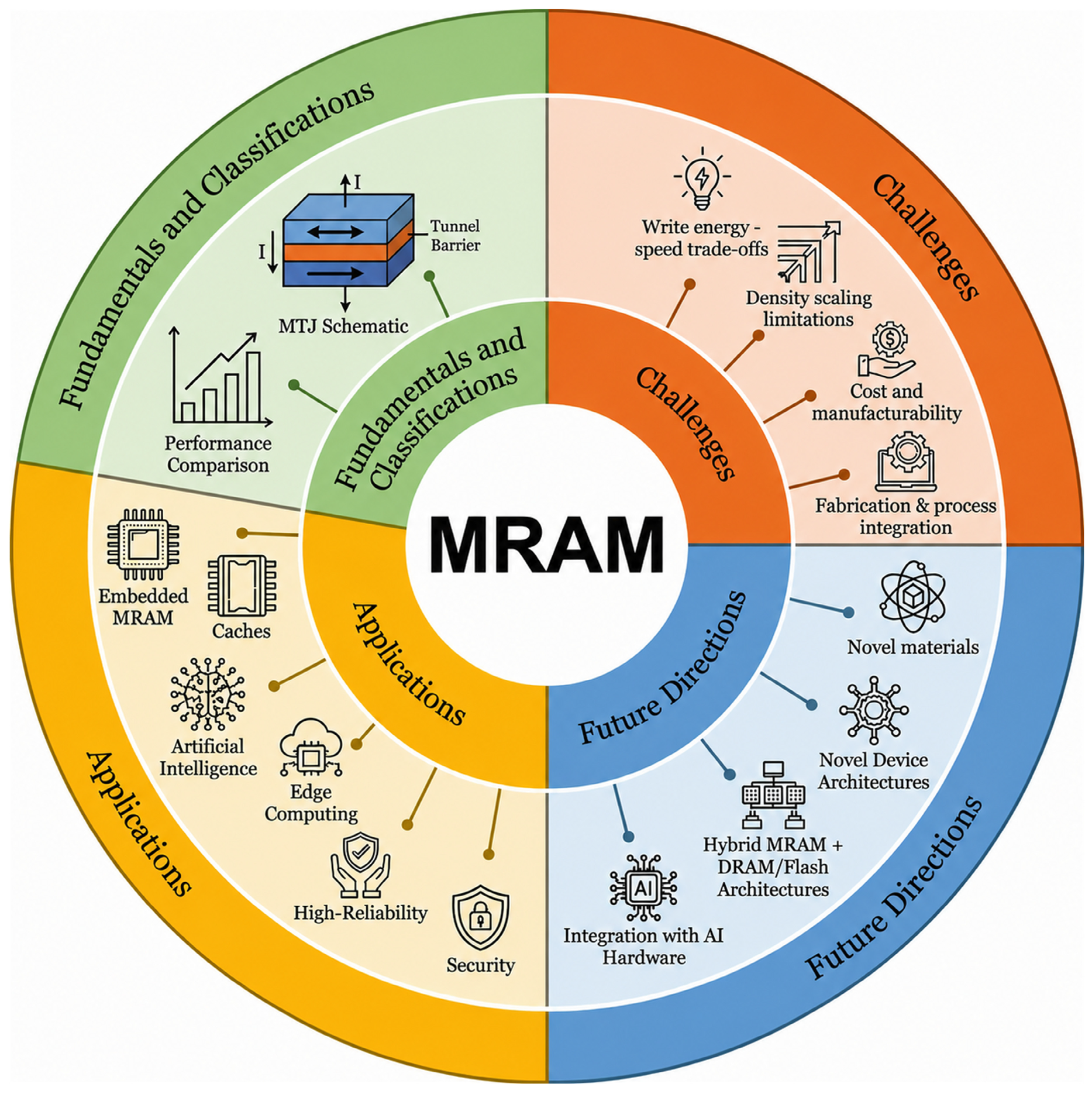
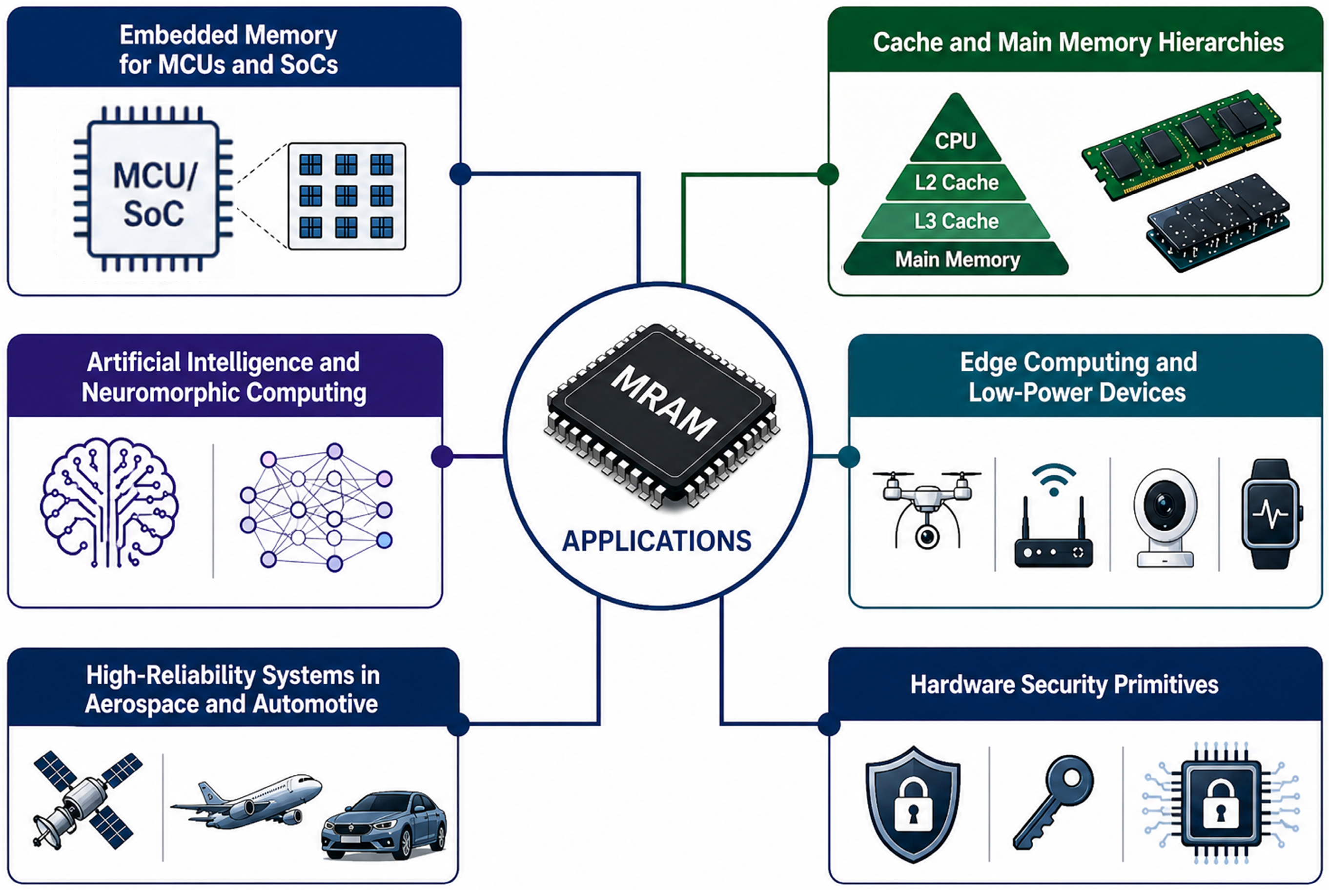
This review aims to systematically trace the developmental trajectory of MRAM technology, provide an in-depth analysis of its physical mechanisms, and comprehensively assess its current research status and future potential across various application scenarios. As shown in Figure 1, we will first elucidate the fundamental principles and classifications of MRAM. We will then delve into specific applications in areas such as embedded systems, standalone memory, and cutting-edge explorations. Finally, we will summarize the key scientific and technological challenges that remain in MRAM development, while also outlining its future evolution path and potential for disruptive applications.

2. Fundamentals and Evolution of MRAM

2.1. Fundamentals of MRAM

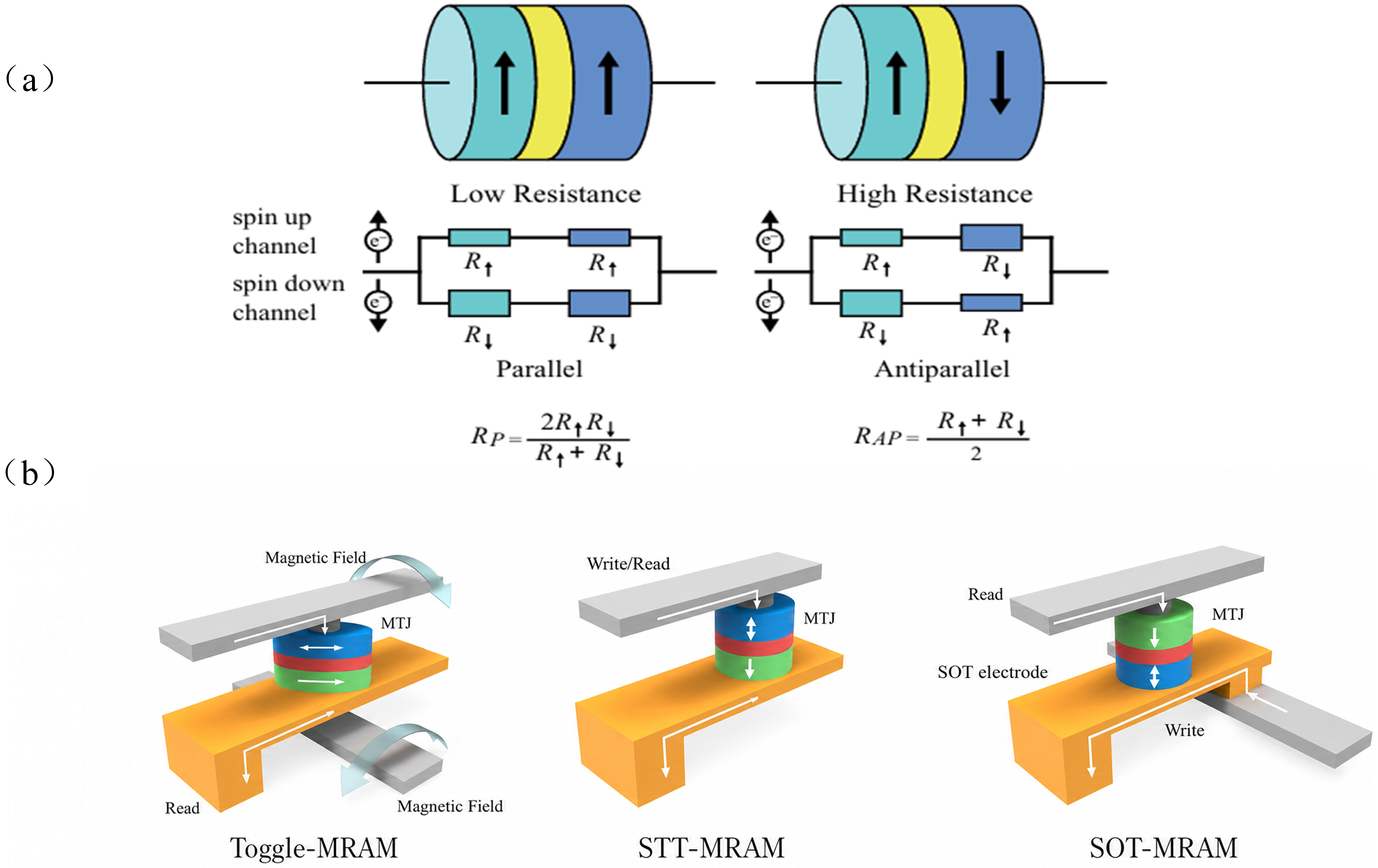
The MTJ comprises a reference layer with fixed magnetization, an insulating tunnel barrier (typically MgO), and a free layer whose magnetization direction can be switched. Data storage in the MTJ is based on the tunnel magnetoresistance (TMR) effect. When the magnetization directions of the reference and free layers are parallel, the electron spins are aligned; this increases the tunneling probability and results in a low-resistance state, denoted as R P in Figure 2a. Conversely, when the magnetizations are antiparallel, the electron spins are misaligned, reducing the tunneling probability and leading to a high-resistance state, R A P . This measurable difference in resistance forms the physical mechanism for storing binary data (“0” and “1”) in MRAM. The TMR, defined by the equation below, is commonly used to quantify this resistance contrast:
T M R = R A P R P R P × 100 %
For MRAM applications, the device merit of an MTJ depends not only on the existence of distinguishable resistance states, but also on two key parameters, namely TMR and the resistance–area product (RA). Early MTJs with amorphous AlOx barriers usually showed room-temperature TMR values below about 70%, resulting in a limited sensing margin and insufficient read robustness. The introduction of crystalline MgO barriers markedly improved the TMR, raising it to about 180% in epitaxial Fe/MgO/Fe junctions [11] and to about 220% in sputtered MgO-based MTJs [12]. Further optimization of CoFeB/MgO/CoFeB stacks, interface quality, and annealing conditions pushed the room-temperature TMR to 604% [13]. The continuous increase in TMR enlarged the resistance window between R P and R A P , thereby improving the sensing margin, read reliability, and error tolerance. RA is defined as the product of the junction resistance and its effective area, usually expressed in Ω · μ m 2 . This parameter determines the effective impedance of the MTJ and directly affects read current, sensing speed, output voltage, and compatibility with CMOS access transistors. Device optimization in MRAM therefore requires a balance between TMR and RA rather than the maximization of either parameter alone. Low-resistance CoFeB/MgO/CoFeB MTJs have achieved a TMR of 138% with an RA of 2.4 Ω · μ m 2 [14]. Perpendicularly magnetized MgO-based MTJs have maintained high magnetoresistance at an RA of about 4.4 Ω · μ m 2 [15]. W-engineered perpendicular MTJs have reported a TMR of 249% with an RA of 7.0 Ω · μ m 2 [16]. For low-RA perpendicular MTJs, the bias dependence of TMR must also be considered, since it further influences the output voltage and effective sensing margin during practical read operation [17]. Overall, the synergistic optimization of high TMR and an appropriate RA constitutes a fundamental device-level prerequisite for enabling high-speed, low-power, and high-reliability MRAM operations.
Figure 2. MRAM working mechanisms based on MTJ structures. (a) Two-channel model of an MTJ, illustrating spin-dependent transport in the parallel (low-resistance) and antiparallel (high-resistance) states, where the total resistance is determined by spin-up and spin-down conduction channels. Reprinted from Ref. [18]. (b) Schematic illustrations of three generations of MRAM technologies: Toggle-MRAM, which uses external magnetic fields for switching; STT-MRAM, which employs spin-transfer torque via a vertical current through the MTJ; and SOT-MRAM, which utilizes spin–orbit torque with separate write and read paths for improved performance. Reprinted from Ref. [19].
Nanomaterials 16 00816 g002

2.2. Evolution of MRAM

MRAM has been developed for more than three decades. Its device structure and working principle have undergone continuous innovation. Figure 2b shows the structural diagrams of three generations of MRAM. Toggle-MRAM, the first generation of MRAM, utilizes magnetic-field-induced switching via orthogonal word-line currents, with a synthetic antiferromagnet (SAF) free layer enabling deterministic Savtchenko toggle switching and effectively suppressing half-select disturbances. From the materials perspective, Toggle-MRAM is typically based on an MTJ stack that includes a pinned magnetic layer, an insulating tunnel barrier, and a SAF-based free layer. AlOx tunnel barriers were commonly used in early field-switched MRAM, whereas MgO-based barriers later became important in the broader development of high-TMR MTJ technologies [20]. The SAF free layer generally consists of two ferromagnetic layers antiferromagnetically coupled through a thin non-magnetic spacer, such as Ru [21]. This coupled configuration is essential for Savtchenko switching, because the magnetizations of the two free-layer components can rotate in a controlled manner under the combined magnetic fields generated by the word and bit lines [22]. Because the write process is driven by magnetic fields rather than by charge trapping or repeated tunneling-current stress, this architecture offers ultra-high endurance and long-term data retention, making it suitable for radiation-hardened and mission-critical applications. Spurred by the promise of universal memory, intensive development of MRAM started in the mid-1990s [23]. Over the past decades, several research groups and industrial laboratories have contributed to the development of this technology [24,25,26,27]. As early as 2003, IBM introduced one of the first MRAM prototypes, characterized by high speed and endurance. In 2006, Freescale began mass production of 4 Mb Toggle-MRAM [28]. However, due to its magnetic-field switching architecture, this technology faced severe scalability limits, with commercial densities remaining much lower than those of mainstream semiconductor memories. It has therefore been mainly adopted by companies such as Honeywell and Cobham/CAES for aerospace and defense applications. The need for large field-generating write currents leads to high power consumption, increased circuit complexity, and poor scalability, ultimately driving the transition to STT-MRAM with superior energy efficiency and density.
Second-generation MRAM leverages the STT effect, in which a spin-polarized current flowing perpendicular to the MTJ plane transfers angular momentum to the free layer, enabling magnetization switching without external magnetic fields and eliminating field-generating write lines. This transition substantially improves cell scalability, energy efficiency, and CMOS integration. The material development of STT-MRAM is closely associated with perpendicular CoFeB/MgO/CoFeB-based MTJs. In a typical perpendicular STT-MRAM stack, the MgO tunnel barrier supports coherent spin-dependent tunneling and thereby provides a high tunnel magnetoresistance ratio [29]. The CoFeB/MgO interface also contributes interfacial perpendicular magnetic anisotropy, which is critical for maintaining thermal stability in scaled perpendicular MTJs [30,31]. The reference layer is often pinned by exchange bias or stabilized using a synthetic antiferromagnetic structure, whereas the free layer stores binary information through its parallel or antiparallel alignment with the reference layer. The physical basis of STT switching is the transfer of spin angular momentum from a spin-polarized current to the free-layer magnetization. During writing, a vertical current passes through the MTJ and becomes spin-polarized by the reference layer [32]. When the current exceeds the critical switching threshold, the spin-transfer torque overcomes magnetic damping and drives the free layer from one stable magnetic state to the other. Therefore, the CoFeB/MgO interface is not only responsible for readout through tunnel magnetoresistance but also strongly affects thermal stability, switching current, and write-error behavior in scaled STT-MRAM devices [29,30,31]. STT-MRAM achieves nanosecond-scale write speed, higher density, and endurance of 1010–1012 cycles, enabling its use as a replacement candidate for embedded Flash and expansion into standalone and persistent memory applications while retaining the standard 1T–1MTJ architecture. A major milestone in the commercialization of MRAM occurred in 2016, when Everspin launched the industry’s first 256 Mb STT-MRAM [33]. In 2019, Samsung began mass production of a 1 Gb embedded STT-MRAM based on a 28 nm FDSOI platform [34]. In 2022, Samsung advanced MRAM to the 14 nm FinFET node [35], while Everspin released 8–64 Mbit SPI-interface MRAM products for industrial Internet of Things (IoT) and embedded applications [36]. As manufacturing processes mature and capacity scales up, MRAM has expanded beyond niche aerospace applications into mainstream markets such as IoT, artificial intelligence, automotive electronics, and persistent memory. Nevertheless, the shared read/write current path of STT-MRAM introduces read-disturb concerns and write-error-rate (WER) challenges. These issues become more pronounced at scaled technology nodes, where reduced thermal stability, MgO barrier reliability, and the trade-off among current density, latency, and retention must be carefully balanced.
SOT-MRAM, regarded as the third generation of MRAM, adopts a three-terminal architecture that decouples read and write paths and enables magnetization switching via SOT generated by in-plane currents in a heavy-metal layer, thereby eliminating read disturbance. In SOT-MRAM, the MTJ is integrated with an additional spin-source layer adjacent to the free layer [37,38]. This spin-source layer is commonly formed using materials with strong spin–orbit coupling, such as Pt, Ta, W, TaW alloy or β-W [39,40,41], and its material properties directly determine the charge-to-spin conversion efficiency, write current density, and Joule heating [38,42]. During writing, an in-plane charge current flows through the spin-source layer and is converted into a transverse spin current through the spin Hall effect or interfacial spin–orbit coupling [37,38]. The resulting spin accumulation at the interface exerts damping-like and field-like torques on the adjacent free layer [40]. These torques enable magnetization reversal without forcing the write current through the MgO tunnel barrier [37,38,39,40,41,42,43,44]. This separation between the lateral write path and the vertical read path is the central device-level advantage of SOT-MRAM, because it suppresses read disturbance and reduces electrical stress on the tunnel barrier [37,38]. However, deterministic field-free switching usually requires symmetry breaking through material, structural, or magnetic design [37,38,39,40,41,42]. In addition, the resistivity of the spin-source layer, interface transparency, spin Hall angle, and electromigration reliability remain critical factors for array-level integration [38,42]. Depending on the orientation of the magnetic easy axis relative to the write current, SOT-MRAM switching can be classified into Type Z (out-of-plane easy axis), Type Y (in-plane transverse easy axis), and Type X (easy axis parallel to the current, typically requiring an assist field), each exhibiting distinct switching dynamics [43]. Among these configurations, Type-Z SOT-MRAM is particularly attractive for high-density memory because its perpendicular magnetic anisotropy is compatible with scaled p-MTJs and provides favorable thermal stability. Its main challenge is deterministic field-free switching, since conventional heavy-metal layers mainly generate in-plane spin polarization. Current approaches therefore employ tilted anisotropy, exchange bias, compositional gradients, or low-symmetry spin-source materials to introduce built-in symmetry breaking or an out-of-plane spin-polarization component [45,46]. Recent van der Waals heterostructures have also demonstrated room-temperature field-free switching through unconventional out-of-plane torque [47]. Further development still requires improvements in wafer-scale growth, thermal robustness, process uniformity, and CMOS-compatible integration [48]. Although SOT-MRAM demonstrates sub-nanosecond switching speed and ultra-high endurance, it remains largely in the research and early development stage due to challenges including high write current density, increased cell footprint, and integration complexity. Since 2018, third-generation SOT-MRAM has gained attention for its separate read/write path and ultrafast switching. Related work from Beihang University and its collaborators has played an important role in advancing SOT-MRAM from device-level studies toward manufacturable technologies: field-free switching of a perpendicular magnetic tunnel junction through the interplay of spin–orbit torque and spin-transfer torque was experimentally demonstrated in 2018 [49], high-performance SOT-MTJ devices were integrated on a 200 mm wafer manufacturing platform in 2022 [50], and a manufacturable 1 Kb SOT-MRAM multiplexer array was further reported in 2023 [51]. In 2025, a collaboration between NYCU, TSMC, and ITRI demonstrated a 64 kb β-phase tungsten SOT-MRAM array achieving ~1 ns switching, over 10-year retention, and thermal stability up to 700 °C—marking a critical step toward practical applications [52]. We have compiled a timeline of MRAM product production and technology development from 2005 to the present in Table 1.

2.3. Performance Comparison

From a technological evolution standpoint, Toggle-MRAM, STT-MRAM, and SOT-MRAM represent successive milestones in the advancement of MRAM technology, each introducing breakthroughs in write mechanisms, power efficiency, integration density, and reliability. Table 2 provides a comparative summary of key metrics across major memory technologies, highlighting the performance, scalability, and integration advantages of STT-MRAM and SOT-MRAM relative to Toggle-MRAM, Flash, DRAM, and SRAM.
In this review, the evolution of MRAM reflects a clear transition from field-driven to spin-transfer-torque-driven to spin–orbit-torque-driven architectures. Toggle-MRAM establishes the industrial foundation with its superior reliability; STT-MRAM achieves a balanced trade-off between density and energy efficiency, enabling large-scale commercialization; and SOT-MRAM approaches the theoretical limits of speed and endurance, positioning itself as a key enabler for next-generation unified memory and computing systems. Future research will likely focus on lowering SOT write energy, achieving higher TMR values, and improving thermal stability, ultimately driving MRAM toward greater capacity, lower power consumption, and broader applicability in emerging computing paradigms.

2.4. Fabrication Process of SOT-MRAM

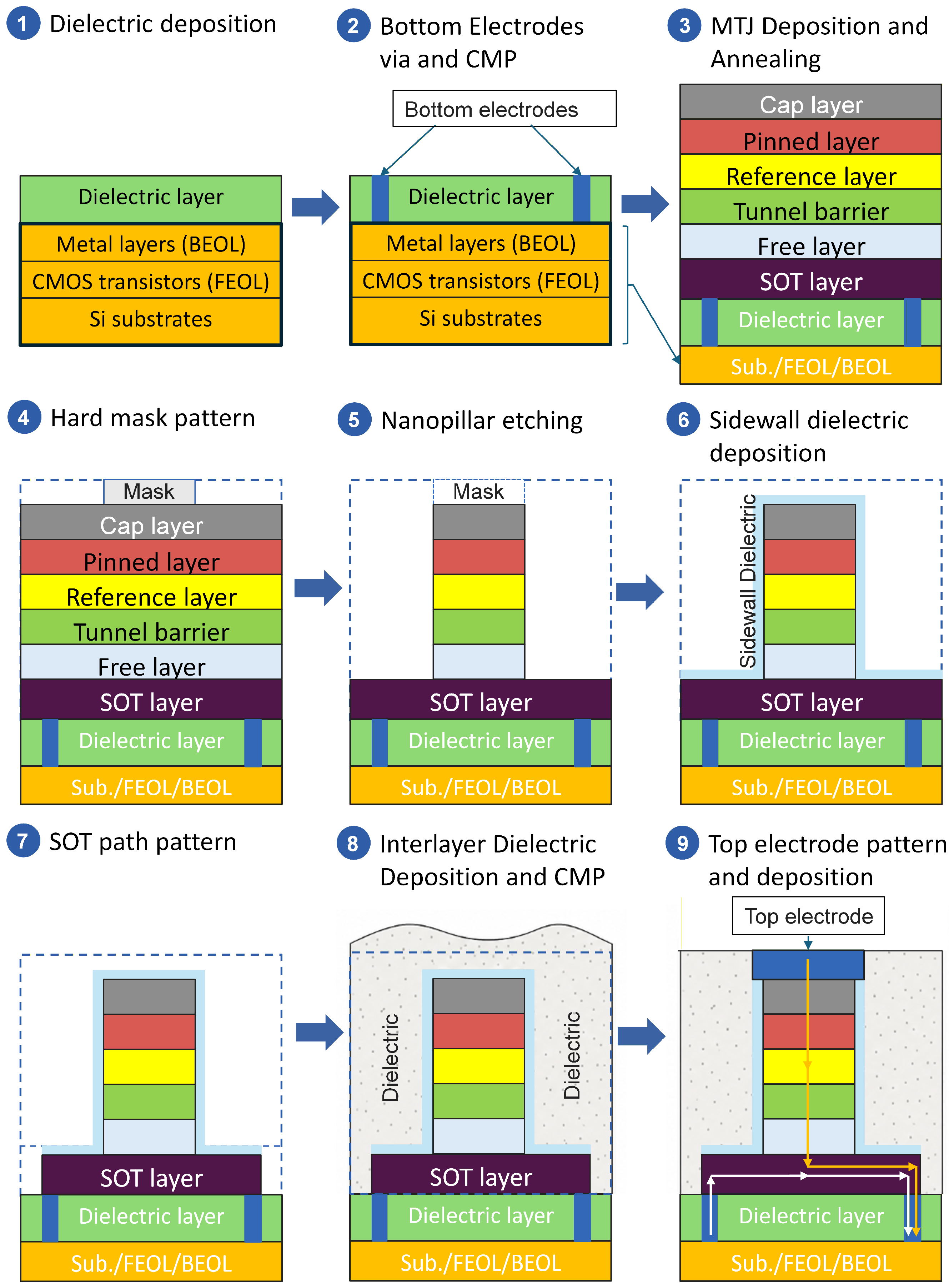
The fabrication of SOT-MRAM involves the hybrid integration of MTJ and CMOS processes. The MTJ fabrication processes can be carried out after the multilevel metal interconnects in the CMOS back-end-of-line (BEOL) are formed. This section focuses on the representative MTJ back-end-of-line process (which may vary across different manufacturers and foundries). Figure 3 shows the typical fabrication process of SOT-MRAM. The key steps are detailed as follows:
Dielectric deposition: After the conventional CMOS process is completed, a dielectric material (SiO2, SiNx) with an appropriate density and thickness is deposited on the Si substrate, where the CMOS transistors (including front-end-of-line (FEOL) devices) and BEOL metal interconnects have already been fabricated, thereby forming a dielectric layer to support the subsequent MTJ devices.
Bottom electrode via and CMP: Bottom electrode via structures are formed by etching, enabling electrical connection between the bottom electrode and the underlying BEOL metal layer; metal is deposited to fill the vias and form the bottom electrode; then, chemical mechanical polishing (CMP) is performed to reduce the surface roughness (ideally below 0.2 nm), providing a flat and high-quality surface for the growth of the SOT-MTJ device, which is essential for ensuring the performance of SOT-MRAM.
MTJ deposition and annealing: Since the SOT layer serves as the path for the write current to generate spin current that drives the magnetization switching of the free layer, SOT-MRAM adopts a top-pinned configuration, in which the pinned layer and reference layer are located near the top electrode, while the free layer is positioned adjacent to the SOT layer. The basic functional layer structure is illustrated in Figure 3③. A multilayer stack including the SOT layer, MTJ layers, and capping layer is deposited by magnetron sputtering. After stack deposition, vacuum annealing is usually performed under a magnetic field for better TMR values. During this step, current-in-plane tunneling (CIPT) measurement is required to monitor key properties of the film stack, such as the TMR ratio and RA.
Hard mask pattern: A dielectric layer, normally SiO2, SiNx, or SiC, is deposited to serve as the hard mask later on. Then, photolithography is performed to define the hard mask pattern, then the hard mask layer is etched, followed by complete removal of the photoresist.
MTJ nanopillar etching: The MTJ multilayer stack is etched and the hard mask is partially (the remaining part will be removed later on) or fully consumed during the etching. The etching process must be precisely stopped above the SOT channel layer, while ensuring that the free layer is completely etched.
Sidewall dielectric deposition: An in situ sidewall dielectric layer is deposited to prevent moisture, oxygen, and other contaminants from degrading the MTJ layers.
SOT layer pattern: Photolithography is performed to define the SOT channel pattern, and then to etch the SOT layer.
Interlayer dielectric deposition and CMP: A dielectric layer is deposited to fill the gaps and isolate the MTJs, then CMP is first performed to planarize the surface.
Top electrode pattern and deposition: An interlayer dielectric layer is deposited, photolithography is performed to define the top electrode via pattern above the MTJ; the dielectric layer is etched to form the top electrode via structure; then the top-electrode metal is deposited. Finally, the SOT-MRAM is ready, and the write current path is indicated by white arrows, whereas the read path is indicated by yellow arrows. Depending on the interconnection requirements, more than one metal layer may be formed after the MTJ. In addition, to meet the functional requirements of chip packaging, wire-bonding pads and a passivation layer need to be formed at the topmost level.

3. Applications of MRAM

The unique combination of non-volatility, high speed, and low power consumption positions MRAM as a versatile technology for a wide range of application scenarios. As shown in Figure 4, we discuss its applications across six representative domains: (1) embedded memory for microcontrollers and SoCs, (2) cache and main memory hierarchies, (3) artificial intelligence and neuromorphic computing platforms, (4) edge computing and low-power devices, (5) high-reliability systems in aerospace and automotive environments, and (6) hardware security.

3.1. Embedded MRAM

In modern SoC design, embedded memory is a critical subsystem that directly affects overall power efficiency, computational performance, and system reliability. With SoC integration levels rapidly increasing and workloads becoming more heterogeneous, embedded memory is expected to deliver not only high-speed access and low power consumption, but also improved non-volatility, area efficiency, and CMOS process compatibility.
Traditionally, SRAM and eFlash have been the two dominant embedded memory solutions. SRAM, featuring nanosecond-level access latency and full CMOS compatibility, is widely adopted in caches and register. However, its 6T structure results in a large cell area and high static power leakage, while the lack of non-volatility prevents data retention upon power loss. eFlash, in contrast, provides power-off data retention, but suffers from slow write operations and high programming voltages. Additionally, it requires 6–7 additional mask layers for fabrication and a dedicated high-voltage module, leading to increased fabrication cost and process complexity and poor compatibility with advanced logic nodes [85,86]. In response to these limitations, STT-MRAM has emerged as a next-generation embedded non-volatile memory (eNVM), combining nanosecond-level access speed, non-volatility, negligible static leakage, and high endurance [85]. MTJs, the key memory cell of MRAM, can be monolithically integrated into the back-end-of-line (BEOL) with only three additional masks, significantly simplifying fabrication compared to eFlash [86,87].
The industrial-grade reliability of embedded STT-MRAM has been validated through silicon demonstrations. In 28 nm FDSOI logic processes, embedded STT-MRAM macros operate over a temperature range from −40 °C to 125 °C, tolerate 260 °C solder reflow, and maintain stable write operation under external magnetic field disturbances up to 550 Oe [87]. Through MTJ stack and patterning optimizations, tunnel magnetoresistance ratios exceeding 200% are achieved, enabling read margins beyond 25σ in 8 Mb macro arrays. Combined reliability assessments verify endurance exceeding 106 write cycles, 1000 h high-temperature retention, and 10-year data retention, while error-correcting codes and redundancy are employed to ensure high yield at the array and system levels [88].
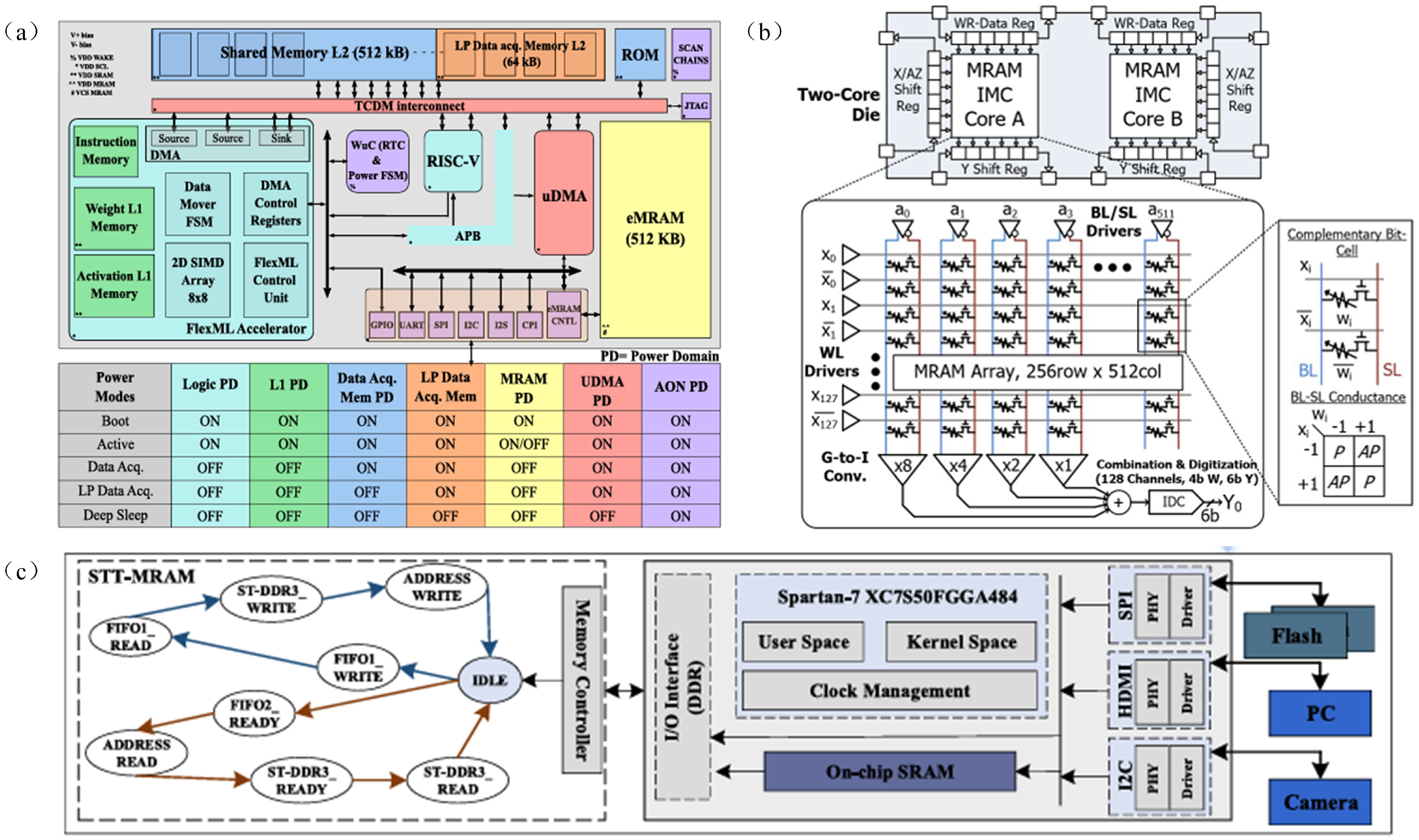
Subsequent technology generations extend these reliability results to higher densities and a wider operating envelope. Shimoi et al. demonstrated a 22 nm, 32 Mb embedded STT-MRAM macro for high-end microcontrollers, featuring 5.9 ns random read, 7.4 MB/s write throughput, and reliable operation up to 150 °C enabled by a boosted cross-coupled sense amplifier and a fast-write scheme [89]. At the system level, in Figure 5a, Jain et al. integrated state-retentive embedded MRAM into the TinyVers heterogeneous machine-learning SoCs as non-volatile storage for boot code and model parameters, enabling aggressive duty cycling with deep-sleep power consumption reduced to 1.7 µW [90].
Beyond conventional storage applications, embedded MRAMs fabricated in advanced technology nodes are increasingly repurposed as compute-capable arrays. At the array operation level, write margin robustness is evaluated through write voltage–access time operating windows. Myung S et al. presented shmoo plots under different operating conditions, showing wide and well-defined pass regions that indicate a sufficient write margin across process, voltage, and temperature variations [91]. Later on, Deaville, P et al. demonstrated a 14 nm MRAM-based multi-bit analog in-memory computing macro in which stacked MTJs implement multi-bit weights, enabling calibrated bit-parallel multiply–accumulate operations with performance reaching 18.29 TOPS/mm2 and energy efficiency of 340.8 TOPS/W in Figure 5b [92]. Deaville et al. further reported a fully row- and column-parallel in-memory computing macro implemented in a foundry 22 nm MRAM, employing differential readout and conductance-to-current conversion to enhance signal-to-noise ratio and robustness against device variability [93]. Beyond reliability-oriented memory operation, recent demonstrations show that MTJ critical dimensions can be scaled below 50 nm while maintaining sub-ppm bit-error rates. Such scaling enables both RAM-like operation with write endurance exceeding 1014 cycles and Microcontroller Unit (MCU)-oriented operation with endurance beyond 106 cycles and data retention exceeding 20 years at temperatures above 150 °C [94]. Recent automotive-grade eMRAM demonstrations further push endurance and energy-efficiency limits, reporting write energies down to 10 pJ/bit and endurance beyond 1012–1014 cycles while supporting reliable operation up to 150 °C [95].
STT-MRAM is also particularly well suited for IoT edge devices and mobile SoCs. As shown in Figure 5c, an STT-MRAM-based instant-on/off system has been demonstrated in low-power IoT nodes, enabling devices to tolerate intermittent power without state loss [96]. In mobile SoCs, STT-MRAM can function as non-volatile caches, tightly coupled memory (TCM), or replacement for fast ROM blocks, reducing static power consumption while preserving performance. Moreover, STT-MRAM-enabled AI/ML accelerators in mobile/edge designs achieve reduced leakage, area savings, and enhanced robustness under process and temperature variation [97].
These use cases further strengthen the argument that STT-MRAM is not just a candidate for embedded control systems, but also a transformative memory solution for low-power IoT and mobile platforms. Embedded STT-MRAM successfully bridges the gap between SRAM’s speed and eFlash’s non-volatility, providing an energy-efficient, scalable, and reliable solution for next-generation SoCs. Its industrial validation and process maturity indicate readiness for deployment in diverse domains, including automotive electronics, industrial IoT, and smart embedded controllers.

3.2. MRAM in Caches and Main Memory

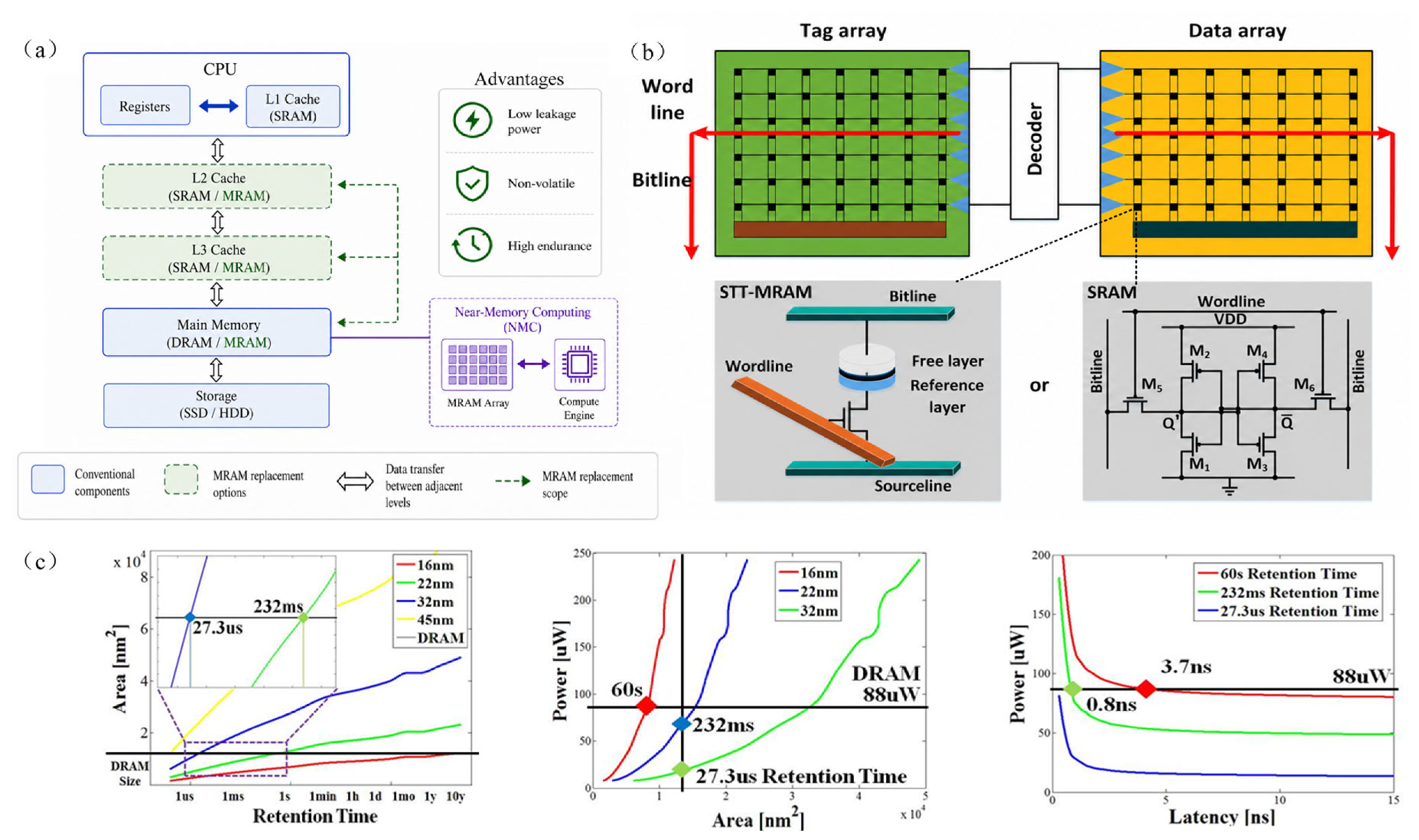
As semiconductor technology scaling approaches its physical and energy limits, cache and main memory subsystems have become dominant determinants of computing system performance and energy efficiency. Traditional SRAM and DRAM technologies, despite their high speed, suffer from static leakage, scalability issues, and inherent volatility under deep submicron processes. Figure 6a illustrates the integration of MRAM within the memory hierarchy, where it serves as a flexible replacement for conventional SRAM in cache levels and a potential candidate for main memory, while enabling near-memory computing to reduce data movement overhead.

3.2.1. L2/L3 Cache Substitution

At intermediate cache levels, STT-MRAM offers a compelling trade-off between energy efficiency, latency, and density. While SRAM provides nanosecond-level speed, its 6T structure induces high static power dissipation, particularly in multi-megabyte on-chip caches. In contrast, STT-MRAM nearly eliminates standby leakage and allows denser array configurations. Simulation-based studies by Zhang et al. indicated that for cache capacities exceeding 32 MB, STT-MRAM achieves an overall 42% reduction in energy consumption compared to SRAM while maintaining comparable access latency [98]. Figure 6b illustrates how STT-MRAM cells can replace conventional SRAM in cache implementations, highlighting their density advantage and the potential for hybrid cache architectures [98]. Experimental implementations further confirm this potential: the Samsung Embedded MRAM macro demonstrates adaptive bias control and ECC-assisted endurance optimization in a 28 nm process, achieving approximately 20% write energy reduction and 15–40% area savings compared with eFlash [85]. Additionally, ROM-embedded STT-MRAM (R-MRAM) structures have been proposed to integrate read-only tables and cache memory into a unified macro, achieving higher bit density without degrading cache-mode access latency—particularly beneficial for microcode or lookup-table applications in L2/L3 caches [88]. Despite these advantages, several critical challenges hinder the large-scale deployment of STT-MRAM as a direct SRAM replacement. In particular, the relatively high write current leads to increased write energy and latency variability, while reliability concerns—including WER, read disturbance, and retention degradation—become more pronounced at scaled technology nodes. Furthermore, the integration of MTJs into standard CMOS processes introduces additional fabrication complexity and cost overhead. These limitations necessitate careful architectural and circuit-level co-optimization rather than straightforward substitution.
The last-level cache (LLC), which in many modern processors corresponds to the L3 cache, represents the most extensively explored use case for MRAM-based storage. Marinelli et al. conducted a comprehensive microarchitectural exploration of STT-MRAM LLC configurations and demonstrated that through optimizing cache associativity, banking, and Miss Status Holding Register (MSHR) management, LLC energy consumption can be reduced by up to 60% with less than 8% performance degradation [100]. Complementary works further exploit perpendicular MTJ (pMTJ) stacks to improve area efficiency and energy scalability in non-volatile LLC implementations [101]. Hybrid cache architectures combining SRAM and STT-MRAM banks have also been widely investigated. By mapping read-dominant data to MRAM while retaining write-intensive blocks in SRAM, these schemes effectively mitigate write-energy and endurance limitations, achieving balanced throughput and reliability [102]. Cheshmikhani et al. proposed a system-level reliability modeling framework that captures the combined impact of multiple error mechanisms, enabling reliability-aware cache management and error-correcting code design [103].

3.2.2. From Main Memory Integration to Near-Memory Storage

Beyond cache-level deployment, MRAM has also been explored as a candidate for non-volatile main memory and near-memory storage. Jin et al. demonstrated that, with circuit-level optimization, STT-MRAM-based main memory systems can reduce total power consumption by up to 66% compared with DRAM while achieving competitive access latency under specific operating conditions [99]. Figure 6c illustrates the optimization trends in area, power, and latency of STT-MRAM by relaxing the retention time, indicating that MRAM can complement or partially replace DRAM in energy-constrained systems.
In accelerator-centric platforms, cross-layer optimization frameworks such as DeepNVM++ have explored the use of STT-MRAM and SOT-MRAM in deep neural network memory hierarchies. Compared with SRAM- and DRAM-based designs, this approach can improve the energy-delay product (EDP) and area efficiency [104]. Similarly, Han et al. proposed an advanced hybrid MRAM-based GPU cache system for graphics processing, achieving up to 28% speed improvement, 56% energy reduction, and 66.45% leakage power optimization, highlighting MRAM’s applicability to high-performance computing workloads [102].
At this stage, MRAM primarily serves as a near-memory storage medium rather than an active computing element. However, its proximity to processing units and intrinsic non-volatility naturally motivate the transition toward more aggressive memory-centric computing paradigms.

3.2.3. MRAM-Based Near-Memory Computing

Building upon MRAM’s successful deployment in cache hierarchies and near-memory storage, recent research has extended its role toward near-memory computing (NMC), in which selected computations are offloaded to memory-adjacent structures to reduce data movement. The energy benefit of NMC originates from the large difference between arithmetic and data-access costs. At the 45 nm technology node, a 32-bit integer addition consumes approximately 0.1 pJ, whereas a 64-bit access to an 8 kB cache requires about 10 pJ and a 64-bit DRAM access consumes approximately 1.3–2.6 nJ [83]. These values vary with the technology node and memory organization, but they show that repeated processor–memory transfers can consume substantially more energy than the arithmetic operation itself.
Unlike storage-centric use cases, MRAM-based NMC emphasizes application-level acceleration by exploiting data locality and non-volatility. Placing computation close to the MRAM array reduces external-memory accesses and the movement of operands and intermediate results. In a representative STT-MRAM-based NMC architecture for sparse matrix–vector multiplication, the optimized readout circuit achieved an energy consumption of 0.242 pJ/bit and a memory bandwidth of 26.7 GB/s. Depending on matrix sparsity, the proposed accelerator reported up to a 64× improvement in energy consumption and up to a 1120× reduction in execution latency compared with the unoptimized implementation [105]. These results are workload- and architecture-dependent, but they provide a quantitative example of the energy savings obtained by reducing data movement and irregular memory accesses.
Representative MRAM-NMC applications include security-aware processing, embedded and IoT systems, neural network inference, intermittent computing, and approximate computing. Near-memory shift-and-rotate operations and data-encrypted computation macros demonstrate high-bandwidth and energy-efficient support for cryptographic workloads [106,107]. In always-on and IoT platforms, MRAM enables state-retentive sleep modes and instant wake-up, significantly extending system lifetime [108]. For neural network inference and energy-harvesting systems, MRAM-NMC architectures reduce external memory access and enable computation recovery under intermittent power supply [109,110]. In addition, approximate computing techniques exploit intrinsic write-accuracy trade-offs in STT-MRAM to achieve further energy savings at the memory level [111,112,113].
These studies illustrate that MRAM has evolved from a device-level memory innovation into a system-level enabler spanning cache hierarchies, main memory, and near-memory computing applications, positioning it as a key building block for energy-efficient heterogeneous SoCs and AI accelerators.

3.3. MRAM in Artificial Intelligence

The application of MRAM in artificial intelligence has progressed from basic functional demonstrations to advanced system integration. Early proof of concept showed that STT-MRAM arrays could perform in situ logic and arithmetic through multi-row activation and current summation, enabling vector operations directly inside memory [114]. The initial results, obtained largely from small-scale test structures and architecture-level simulations, indicated that MRAM could serve functions beyond conventional storage, motivating further compute-in-memory (CIM) research. During the same period, MRAM was also explored as a synaptic device for neuromorphic computing, drawing on its non-volatility and CMOS compatibility.
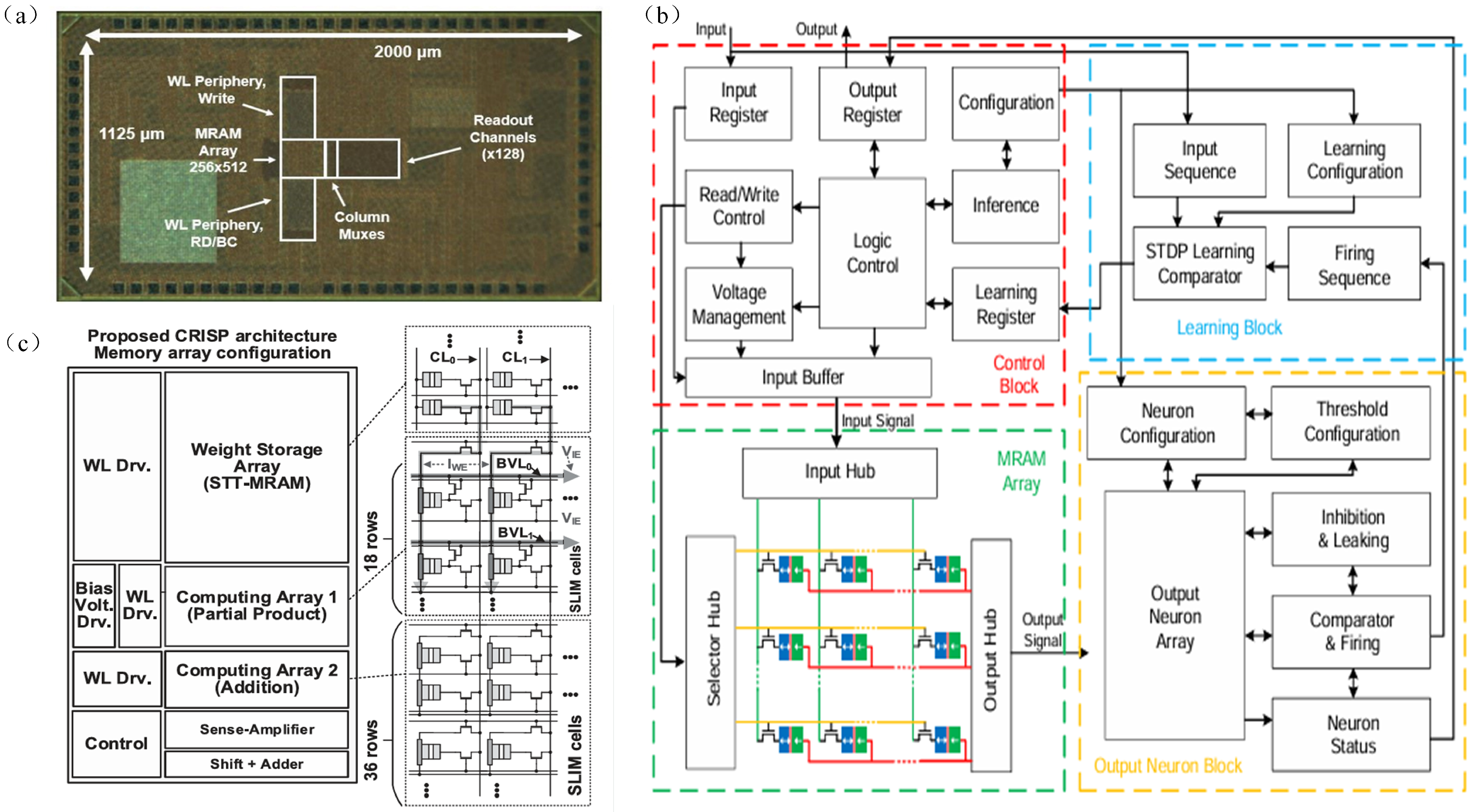
Hardware demonstration and architectural diversification saw the first fabricated STT-MRAM CIM macros and a wealth of architecture-level proposals. Prior to silicon validation, simulation-based studies, such as Stoch In-Memory Computing (IMC) [115] and cross-layer analyses of STT-MRAM IMC, provided early performance projections and design insights that helped to guide subsequent hardware implementations [116]. As shown in Figure 7a, a 128 kb maximally row-parallel MRAM IMC macro was fabricated in a 22 nm FD-SOI process. The macro achieves 5.1 TOPS/W and 758 GOPS/mm2 while maintaining 90% CIFAR-10 inference accuracy, providing silicon-level evidence for large-scale MRAM-based AI accelerators [117]. In neuromorphic computing, fabricated MRAM synaptic arrays and neuron circuits have also been reported. For example, STT-MRAM devices were used to demonstrate spike-timing-dependent plasticity (STDP) [118], while stochastic MRAM switching enabled unsupervised STDP learning with 90% MNIST accuracy [119]. As shown in Figure 7b, the integrated MRAM-based neuromorphic architecture consists of a control block, an STDP-based learning block, an MRAM synaptic array, and output neuron circuits. Furthermore, MRAM synapses with multi-level weights achieved <3% MNIST error [120]. Concurrently, a number of CIM architectures were introduced at the design and simulation level. The NAND-SPIN architecture organized MRAM bit-cells into a NAND-like structure with page-wise activation for parallel CNN inference [121]. The SLIM and CRISP schemes employed SOT-MRAM to perform analog-to-digital conversion (ADC)-free matrix multiplication [122] as shown in Figure 7c, where the CRISP architecture integrates weight storage and computing arrays to enable in-memory multiplication and accumulation without ADC. A time-domain STT-MRAM CIM approach encoded logic and accumulation as pulse widths on shared bitlines [123]. The SIMPLY+ framework targeted improved read margin and lower bit-error rates under device variability [124]. In 2025, the Falcon event-driven object-tracking SoC, fabricated in 28 nm FDSOI technology, integrated heterogeneous MRAM computing blocks—processing-in-memory (PIM) for CNN encoders and NMC for attention-flow processing—and reached macro and system energy efficiencies of 750.18 TOPS/W and 16.34 TOPS/W [125].
These developments show that MRAM has evolved from a storage technology into a capable platform for energy-efficient AI computation. Through co-design across materials, circuits, and algorithms, researchers have demonstrated scalable and reliable MRAM-based neuromorphic systems, and ongoing work on device–circuit–algorithm synergies is expected to further expand the role of MRAM in brain-inspired computing.

3.4. MRAM for Edge Computing and Wearables

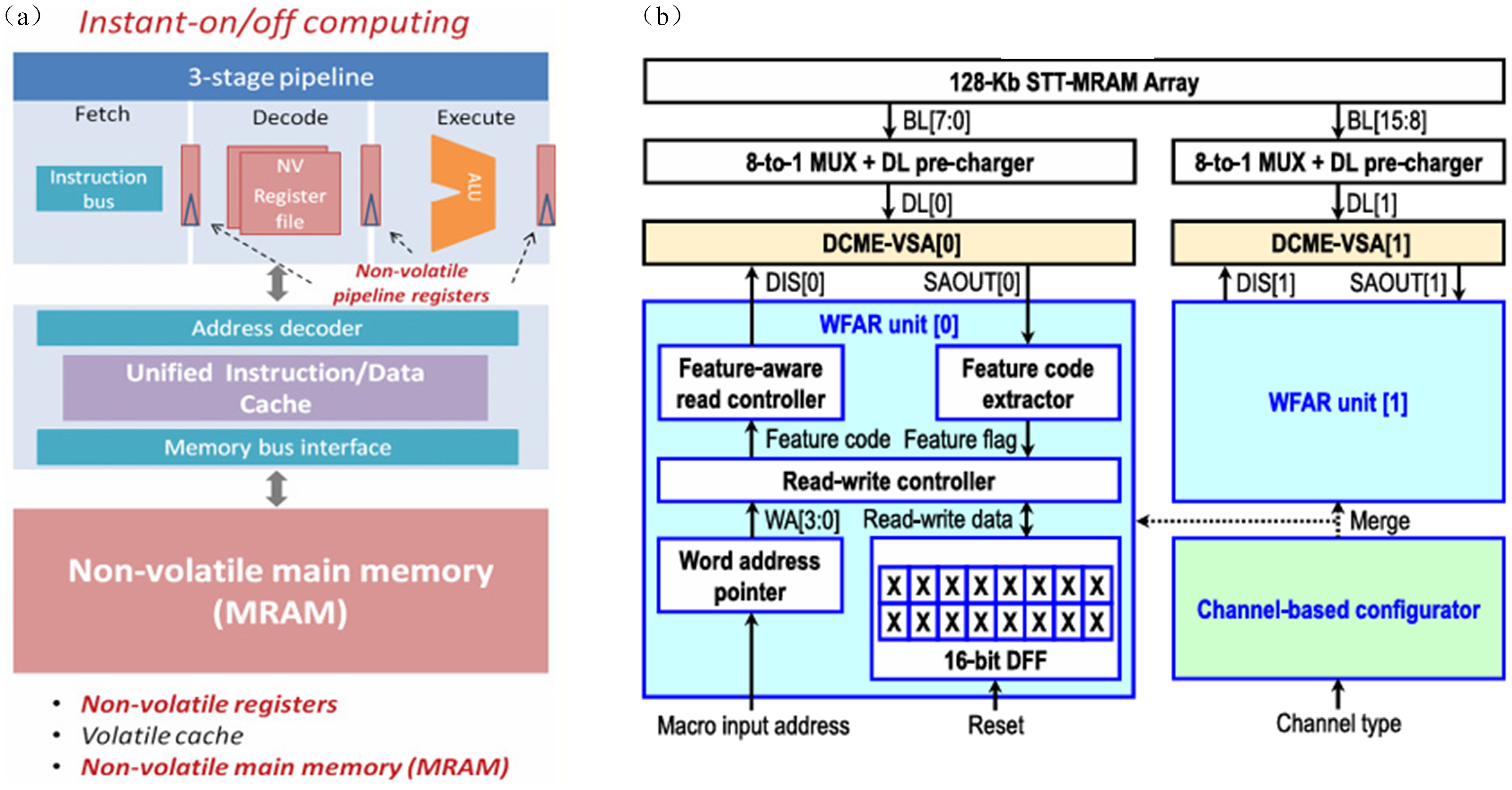
Edge computing requires memory systems that combine ultra-low standby power, fast wake-up/restore capability, and non-volatility. MRAM naturally meets these requirements, offering zero standby leakage, high endurance, and instant data retention without power, making it highly suitable for energy-constrained IoT and wearable devices. In scenarios such as energy-harvesting or battery-limited nodes, frequent power interruptions necessitate rapid system recovery with minimal overhead. Non-volatile processor (NVP) architectures based on MRAM address this challenge by backing up processor states before power loss and restoring them upon wake-up, thereby significantly reducing energy consumption and latency associated with state recovery [126]. As illustrated in Figure 8a, MRAM is integrated into the processor pipeline as non-volatile registers and main memory, allowing instruction states, register contents, and intermediate execution data to be retained across power interruptions, thereby enabling instant system resumption. This establishes MRAM as a fundamental building block for reliable instant-on/off operation in edge computing systems.
Beyond system-level power management, MRAM also enables efficient data processing close to memory, which is critical for edge-AI workloads. An NMC architecture based on STT-MRAM demonstrates substantial improvements in data throughput and computational efficiency, achieving up to 64× energy efficiency gains and over three orders of magnitude latency reduction for sparse workloads [105]. Similarly, SOT-MRAM-based PIM architectures have been proposed to support compressed deep neural network (DNN) inference in resource-constrained environments, reducing data movement overhead while maintaining high computational efficiency [128]. These architectures highlight the role of MRAM in enabling low-power, high-efficiency AI processing directly within edge devices.
Recent hardware implementations further validate the practicality of MRAM in real-world edge platforms. The Vega SoC, designed for IoT end-nodes, integrates on-chip MRAM to support state-retentive sleep modes and near-sensor DNN acceleration, achieving ultra-low-power cognitive wake-up and fully on-chip inference [129]. In addition, an 8 Mb STT-MRAM NMC macro has demonstrated energy-efficient edge-AI inference using sparsity-aware techniques within a compact embedded system [127]. In Figure 8b, the STT-MRAM near-memory computing macro integrates MRAM arrays with feature-aware read controllers and channel-based configurators, enabling data access, feature extraction, and accumulation operations to be performed directly within the memory macro. At a higher level of integration, the Siracusa heterogeneous XR processor incorporates an MRAM-based neural engine tightly coupled with on-chip MRAM memory, achieving significant improvements in both throughput and energy efficiency, compared to off-chip memory solutions [130]. These system-level designs collectively demonstrate that MRAM can be effectively integrated into edge-AI platforms, enabling scalable and energy-efficient computation under strict power constraints. However, such gains are often workload-dependent, and many designs remain at the architecture or simulation level, with limited validation across diverse real-world edge scenarios.
Overall, the convergence of non-volatile system design, near-memory computing architectures, and MRAM-enabled edge processors indicates that MRAM is not only a memory technology but also a key enabler of efficient edge computing. Nevertheless, practical applications still require further optimization, particularly in reducing write energy and latency under high-frequency workloads, improving tolerance to device variability and reliability issues, and achieving cost-effective integration with CMOS technologies. Continued progress in device–circuit–architecture co-design is therefore essential to fully realize the potential of MRAM in next-generation intelligent edge systems.

3.5. MRAM in High-Reliability Domains

In aerospace, military, and automotive systems, memory components must survive harsh radiation, extreme temperatures, and vibrations and demand ultra-high endurance and data integrity. Conventional memories are vulnerable to single event upsets (SEUs), total ionizing dose (TID) degradation, and limited endurance. MRAM, by virtue of its magnetic storage mechanism, demonstrates intrinsic immunity to many radiation effects, virtually unlimited cyclic endurance, and robust performance under extreme conditions—making it a leading candidate for high-reliability non-volatile memory in such demanding applications.
One of the most compelling advantages of MRAM is its resilience to radiation. MTJs are inherently insensitive to charge-based disruptions, making them resistant to SEUs. Montoya et al. experimentally validated that nanoscale MTJs retain their switching and TMR characteristics after high-dose gamma and neutron irradiation, confirming their robustness in radiation environments [131]. Everspin’s commercial MRAM is independently tested to endure >1 Mrad without inducing hard errors and shows SEL tolerance to Linear Energy Transfer (LET) at approximately 84 MeV·cm2/mg. Their radiation-hardened offerings are positioned for aerospace and defense markets. Katti et al. described MRAM devices designed with radiation-hard circuits and high cycling endurance, tailored for space missions [132]. Honeywell also promotes radiation-hardened MRAM ICs for spacecraft use, citing their ability to resist ionizing environments for boot code, configuration memory, and data logging. Avalanche Technology’s “Space Grade” MRAM devices have passed NASA heavy-ion tests up to 1 Mrad without parameter degradation, Single Event Latch-up (SEL) LETth > 85.4, Single Event Functional Interrupt (SEFI) thresholds >120, and no permanent faults post-irradiation.
MRAM demonstrates a compelling combination of radiation resistance, near-unlimited endurance, retention across temperature extremes, and mechanical robustness, making it ideally suited for high-reliability domains such as aerospace, military, and automotive electronics. Though trade-offs remain (density, cost, and integration), MRAM’s unique physics give it a distinct advantage over charge-based memories in mission-critical, harsh-environment systems.

3.6. MRAM in Security Applications

With the growing demand for hardware-level security in IoT, edge AI, automotive, and defense-grade systems, MRAM has emerged as a compelling platform for implementing cryptographic primitives, particularly Physical Unclonable Functions (PUFs) and True Random Number Generators (TRNGs). Unlike charge-based memories, MRAM’s stochastic magnetization switching and thermal noise properties offer natural entropy sources suitable for generating secure keys and random numbers. Furthermore, MRAM’s non-volatility, process compatibility, and robustness against environmental fluctuations make it highly attractive for secure boot, identity authentication, key storage, and anti-tampering applications.
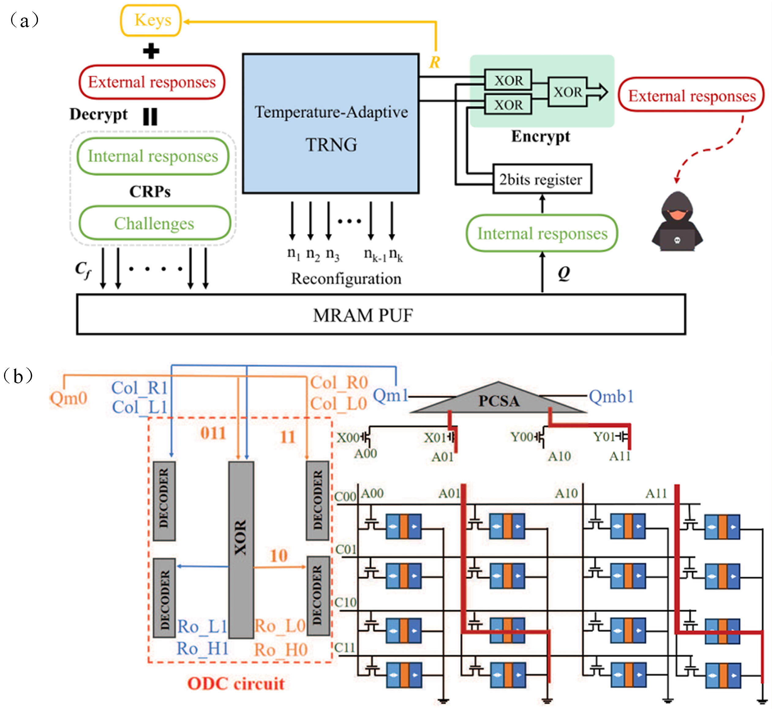
In the domain of random number generation, Suresh et al. developed a high-entropy STT-MRAM TRNG that exploits thermally induced variations in MTJ switching latency to achieve entropy rates approaching 1 bit per sample, while satisfying NIST SP800-22 and AIS-31 statistical test suites under process, voltage, and temperature variations [133]. Similarly, Dai et al. proposed a temperature-adaptive TRNG-encrypted MRAM-PUF architecture, in which intrinsic PUF responses are dynamically masked by TRNG-generated randomness to improve resistance against machine-learning-based modeling and replay attacks in thermally unstable environments [134]. In Figure 9a, the TRNG is tightly coupled with the MRAM-PUF, where the internally generated responses are encrypted through XOR-based operations before being exposed externally, while reconfiguration signals derived from the TRNG continuously perturb the challenge–response mapping. The design, validated in a 65 nm CMOS process using a compact 2T–1MTJ cell, demonstrates strong randomness and improved robustness while maintaining sub-5 μW power consumption suitable for ultra-low-power edge devices.
In parallel, MRAM-based PUF designs have been extensively explored to enhance hardware security. Adel et al. demonstrated an MRAM-PUF architecture with improved resistance to deep-learning-based attacks, where the prediction accuracy approaches random guessing for binary responses [136]. Wu et al. further proposed a double-layer dynamic challenge cross-selection STT-MRAM PUF in Figure 9b, where an obfuscation decode circuit (ODC) is inserted between two MRAM arrays to increase the nonlinearity of the challenge–response relationship, thereby improving robustness and security [135]. In addition, Lee et al. demonstrated spintronic PUFs based on field-free SOT switching, which provide stable responses under thermal stress and process variations [137]. These studies collectively demonstrate that MRAM-based PUFs can achieve both high entropy and strong resistance to modeling attacks.
MRAM’s inherent physical randomness, thermal fluctuation, and process-induced variability, once considered design challenges, are now actively leveraged for robust, lightweight, and tamper-resistant hardware security primitives, positioning MRAM as security-enabling memory beyond mere data storage.

4. Challenges

Despite being widely regarded as a promising cornerstone of next-generation memory technologies—owing to its intrinsic advantages such as non-volatility, high-speed operation, and theoretically high endurance—MRAM continues to confront a set of deeply rooted, multifaceted challenges that hinder its transition from niche markets to widespread commercial deployment. These challenges arise primarily from the unique interplay between MRAM’s physical switching mechanisms, complex material systems, and process integration constraints. Broadly, they can be categorized into four fundamental and interdependent domains that collectively define the current technological bottlenecks impeding large-scale MRAM commercialization.

4.1. The Inherent Trade-Offs in Write Performance

A fundamental limitation in MRAM technology lies in the conflicting requirements between write speed and energy efficiency. STT-MRAM, for example, requires a high current density to induce STT sufficient for deterministic magnetization reversal in nanosecond-scale timeframes. However, this directly results in excessive dynamic power consumption, which undermines MRAM’s energy advantage in low-power systems [138]. Conversely, reducing write current to save energy increases switching latency and worsens the WER, especially in scaled nodes where thermal stability becomes weaker [53]. This trade-off is rooted in the stochastic nature of spin-torque switching: a lower write current reduces the spin angular momentum delivered to the free layer, making the switching process more susceptible to thermal fluctuations and process-induced variations in anisotropy, resistance-area product, and critical current [139]. This speed–power paradox remains a core bottleneck in reconciling MRAM’s theoretical performance benefits with practical deployment in energy-constrained systems such as mobile devices, IoT nodes, and edge-computing platforms. Recent studies further confirm this inherent trade-off: experimental characterizations of perpendicular STT-MRAM report that lowering write current increases the probability of thermally activated failures and broadens the switching-time distribution [140], while device-level analyses show that scaled MTJs require even higher current densities to maintain acceptable energy barriers, exacerbating power penalties [141]. Moreover, write-reliability modeling indicates that sub-nanosecond switching under low-voltage bias dramatically elevates the WER tail, limiting applicability in energy-limited systems [53]. The dependence of WER on write voltage and MTJ size further indicates that aggressive scaling narrows the reliable write window of STT-MRAM [139]. Reference-layer stray fields can also distort the energy landscape of perpendicular MTJs and increase write-error probability, especially in scaled devices [142]. Therefore, write optimization cannot be treated only as a circuit-level problem; it requires co-optimization of the magnetic free layer, tunnel barrier, write pulse scheme, and error-tolerant architecture [140,141,142].

4.2. Process Compatibility and Integration Complexity

Although MRAM is often promoted as a CMOS-compatible memory, real-world implementation reveals non-trivial integration challenges, especially at advanced nodes. The fabrication of MTJs—the key storage elements in MRAM—requires specialized materials such as CoFeB and MgO and demands tight process control of ultra-thin layers (<2 nm) to ensure tunneling magnetoresistance consistency and thermal stability [141]. These steps are typically inserted during the BEOL stage, introducing contamination risks and yield loss when co-integrated with logic transistors [143]. In practice, MRAM integration is not merely the insertion of an additional memory layer; it requires precise control of magnetic multilayer deposition, interface roughness, sidewall damage during etching, post-etch cleaning, and annealing conditions [32]. Small deviations in MgO thickness, CoFeB crystallization, or reference-layer coupling can translate into large distributions in resistance, TMR, switching current, and retention [141]. Furthermore, the need for additional lithography masks, annealing steps, and magnetic shielding in SOT-MRAM further complicates process flows and increases fab cost [144]. For emerging FinFET or gate-all-around (GAA) platforms, MRAM integration is even more constrained due to limited thermal budgets and metal pitch congestion, limiting design flexibility in high-density SoCs. These challenges are particularly pronounced for SOT-MRAM, where the spin-source layer must simultaneously provide high charge-to-spin conversion efficiency, low resistivity, BEOL thermal stability, and compatibility with dense interconnect routing [145,146]. The 300 mm integration of SOT-MRAM has demonstrated the feasibility of CMOS-compatible fabrication, but it also highlights the need to control SOT material stacks, patterning damage, and array-level process uniformity [145]. Field-free perpendicular SOT-MRAM further requires additional symmetry-breaking designs, which increase integration complexity compared with conventional two-terminal STT-MRAM [146].

4.3. Cost, Yield, and Commercialization Challenges

Another critical issue is cost-effectiveness and manufacturing yield. While MRAM benefits from shrinking cell sizes in theory, in practice, the write current scaling is suboptimal, and the MTJ stack thickness cannot be reduced below physical thresholds (typically 1–1.5 nm) without sacrificing data retention [147]. These constraints hinder the adoption of aggressive scaling, limiting MRAM’s competitiveness against mature alternatives like embedded Flash, RRAM, or even DRAM in terms of bit cost per mm2 [148]. In addition, low write margins and process variation sensitivity often necessitate error-correcting codes or redundancy schemes, which further reduce usable yield and increase area overhead [149]. From a commercialization perspective, MRAM must compete not only on intrinsic device metrics, such as speed and endurance, but also on macro-level yield, peripheral-circuit overhead, test cost, and qualification reliability across temperature and lifetime conditions [32]. As a result, the unit cost of MRAM chips remains high, especially in high-density configurations, delaying market penetration beyond niche applications. This is one reason why current MRAM adoption is strongest in embedded non-volatile memory, automotive microcontrollers, industrial systems, and specialty memories, whereas direct cost-per-bit competition with high-density DRAM or NAND Flash remains difficult [32].

4.4. Physical and Architectural Limits to Density Scaling

MRAM scaling is ultimately limited by fundamental spintronic and magnetic material constraints. For instance, as cell sizes shrink, the thermal stability factor Δ (proportional to volume) decreases, resulting in increased susceptibility to spontaneous switching and retention loss, especially at high temperatures. In single-digit-nanometer MTJs, shape anisotropy has been revisited as a possible route to improve thermal stability, but it also introduces new constraints on material design, patterning accuracy, and switching current control [150]. This imposes a trade-off between switching energy, data retention, and device reliability, which becomes more severe in sub-20 nm nodes. Additionally, dipolar field interactions and write disturb effects become prominent in densely packed MTJ arrays, requiring complex shielding or isolation strategies [53]. Reference-layer stray fields and neighboring-cell magnetic interactions can further modify the switching probability and WER distribution in scaled perpendicular STT-MRAM arrays [142]. From an architectural perspective, multi-level cell designs are difficult to implement reliably in MRAM due to its binary switching nature, further limiting its density roadmap relative to NAND Flash or DRAM. Consequently, MRAM still falls short of delivering multi-gigabit density in cost-competitive formats.

5. Future Directions and Opportunities

The future development of MRAM is being driven by coordinated advances across materials, devices, architectures, and system-level integration. Several key research directions are emerging.

5.1. Exploration of New Material

Recent progress in MRAM has been strongly driven by advances in spintronic materials, particularly those enhancing spin–orbit torque efficiency and reducing switching energy. Emerging materials such as heavy metals and topological insulators with large spin Hall angles, orbital Hall materials, and engineered multilayer stacks enable lower write current and faster switching. Weyl semimetals and antiferromagnetic materials are also being investigated as alternative sources of spin–orbit torque because of their unconventional electronic structures, interfacial spin accumulation, or symmetry-dependent spin polarization [151]. For SOT-MRAM, the key material challenge is no longer only to maximize the spin Hall angle, but also to balance charge-to-spin conversion efficiency, resistivity, interface transparency, thermal stability, and compatibility with back-end-of-line processing [152]. In addition, two-dimensional magnetic materials and van der Waals heterostructures are being explored for ultra-scaled MRAM devices with improved tunability and energy efficiency [153,154]. Graphene, h-BN, transition-metal dichalcogenides, and van der Waals magnets may function as tunnel barriers, spin-filter layers, magnetic electrodes, or interface-engineering layers. Their atomically thin structures and dangling-bond-free interfaces provide opportunities for reducing interfacial disorder and electrically controlling spin transport and magnetism [155,156]. Orbitronic materials, which exploit orbital angular momentum rather than only spin angular momentum, provide another emerging route for generating angular-momentum currents in materials that may not possess strong spin–orbit coupling [157]. The generated orbital current can be converted into spin angular momentum in an adjacent magnetic layer and exert an orbital torque on the magnetization [158].
Despite these advances, most MRAM concepts based on two-dimensional and quantum materials remain at the material, single-device, or proof-of-concept stage. Wafer-scale synthesis, interface contamination, environmental and thermal stability, device-to-device reproducibility, nanoscale patterning, and CMOS back-end compatibility remain major barriers to large-scale memory integration [155,156]. These developments suggest that future improvements will increasingly rely on material–device co-optimization to overcome fundamental energy–speed trade-offs. Therefore, future MRAM material research is expected to move from simple material substitution toward interface-level and stack-level engineering, where magnetic anisotropy, damping, spin transparency, and thermal robustness are optimized simultaneously.

5.2. Novel Device Architectures

In parallel with material innovation, MRAM device architectures continue to evolve toward higher performance and scalability. Field-free SOT-MRAM, canted magnetization structures, and two-terminal SOT devices have demonstrated improved write efficiency and simplified integration [159,160]. Among these directions, field-free SOT switching is particularly important because practical SOT-MRAM arrays cannot rely on an external magnetic field for deterministic operation [161]. Meanwhile, perpendicular magnetic anisotropy (PMA) and composite free-layer designs further enhance thermal stability and scalability at advanced nodes [162]. Beyond conventional two-terminal STT-MRAM and three-terminal SOT-MRAM, future devices may also employ hybrid STT–SOT switching, voltage-assisted switching, or engineered free-layer structures to reduce write energy without sacrificing retention. These emerging device concepts provide a flexible foundation for extending MRAM into high-speed cache and embedded memory applications. However, their practical value will depend on whether device-level advantages can be preserved after array integration, where cell footprint, selector design, write disturbance, thermal budget, and peripheral-circuit overhead become equally important.

5.3. Integration with AI Hardware

MRAM is increasingly being integrated into AI hardware platforms, particularly in edge-AI processors and CIM architectures [163]. Recent silicon demonstrations of MRAM-based near-memory computing processors and heterogeneous AI systems have shown substantial improvements in energy efficiency and latency for real-time inference workloads [130]. These results indicate that MRAM is moving beyond conventional non-volatile storage and becoming an important component in energy-efficient AI hardware. Future MRAM-AI integration is expected to focus on edge and embedded inference, where low standby power, fast wake-up, and local weight storage are critical. Non-volatile memory technologies can reduce leakage energy and provide efficient on-chip storage for neural network parameters [164]. MRAM is also attractive for normally-off and always-on intelligent systems because model weights and system states can be retained without refresh power. Recent heterogeneous SoC studies further show that tightly coupled MRAM-based memory near neural engines can improve throughput and energy efficiency [130]. Another key direction is MRAM-based near-memory AI acceleration. A 22 nm nonvolatile AI-edge processor using a 47.25 Mb compressed-computing STT-MRAM macro achieved 21.4 TFLOPS/W, demonstrating the potential of large-capacity MRAM macros for energy-efficient edge inference [163]. In addition, binary, ternary, and low-bit-width neural networks are more compatible with MRAM-based accelerators because they can better tolerate device variation and limited resistance precision [165]. Future research should therefore emphasize device–circuit–architecture co-optimization, variation-aware mapping, low-power sensing, flexible precision support, and heterogeneous memory hierarchy design [164]. MRAM is more likely to complement existing GPU- and SRAM-based AI hardware as a non-volatile, low-standby-power, and instant-on memory component rather than directly replacing them.

5.4. In-Memory Computing

In-memory computing provides a further direction for MRAM-based hardware acceleration. More recently, MRAM crossbar arrays have been experimentally demonstrated for in-memory computing, showing that MRAM can support analog multiply–accumulate operations by exploiting resistance-state summation rather than acting only as a passive non-volatile storage element [166]. Unlike near-memory computing, where computation is performed by logic located adjacent to the memory array, MRAM-based in-memory computing executes selected arithmetic or logic operations directly within the array, further reducing the movement of weights, operands, and intermediate data [167]. These results indicate that MRAM is transitioning from a passive storage element to an active computing medium, where device characteristics, circuit design, and algorithm robustness must be jointly optimized. Analog MRAM-based IMC provides high parallelism and energy efficiency but remains sensitive to resistance variation, read noise, low device resistance, and analog-to-digital conversion overhead [167]. Digital MRAM-based IMC offers higher numerical precision and robustness, although additional sensing, digitization, accumulation, and control circuits increase circuit complexity and hardware overhead [168].
Therefore, future MRAM-based IMC will require device–circuit–algorithm co-design, improved read margin, reduced write energy, variation-aware training, flexible numerical precision, and scalable integration with CMOS peripheral circuits.

5.5. Hybrid Architectures

Due to current density and scalability constraints, MRAM is increasingly considered in hybrid memory and computing systems. In such systems, MRAM serves as a non-volatile buffer or fast log layer, while DRAM or Flash provides bulk storage capacity. This organization improves the balance among data retention, boot-up latency, and endurance in SoCs, especially for edge-computing applications. At the memory-system level, hybrid architectures are attractive because they allow MRAM to be placed where its non-volatility, low standby power, and high endurance provide the greatest system-level benefit, rather than forcing it to compete directly with DRAM or NAND Flash on raw bit density. Hybrid cache and memory hierarchies can combine the low write latency of SRAM, the density advantage of STT-MRAM, and the capacity advantage of DRAM or Flash, thereby reducing leakage power while avoiding the write-energy penalty of using MRAM for all memory levels [169]. At the architecture level, RRAM/MRAM hybrid computing-in-memory architecture integrates heterogeneous memory media through cross-array data buffering and bitwise fusion mechanisms. A dynamic system control module enables adaptive switching between high-energy-efficiency and high-accuracy computing modes, thereby alleviating the performance bottlenecks of single-memory-medium designs. Hybrid architectures also introduce new design problems, including data placement, wear balancing, memory consistency, compiler support, and runtime scheduling. Future work should therefore treat MRAM not only as a device replacement, but as part of a heterogeneous memory hierarchy co-designed with software and workload characteristics.

5.6. Commercialization Landscape and Ecosystem Growth

The commercialization of MRAM has progressed rapidly, with embedded STT-MRAM already deployed in automotive and IoT microcontrollers. Foundries have demonstrated mature eMRAM technologies at advanced nodes, while ongoing development of SOT-MRAM aims to achieve SRAM-class performance for high-speed application. At the same time, the MRAM ecosystem—including design tools, IP support, and manufacturing infrastructure—is expanding, facilitating broader adoption in both edge and high-performance computing systems. This ecosystem-level progress is important because MRAM commercialization depends not only on MTJ performance, but also on qualified process design kits, reliable memory compilers, built-in self-test schemes, error-correction support, and long-term reliability qualification. In the near term, the most realistic commercial path for MRAM is likely to be application-specific deployment in embedded non-volatile memory, industrial and automotive microcontrollers, radiation-tolerant systems, and low-power edge devices. In the longer term, if SOT-MRAM and related material platforms can reduce write current while maintaining manufacturability, MRAM may expand toward high-speed cache, compute-near-memory, and normally-off computing platforms.

6. Conclusions

MRAM exhibits strong potential for future memory and computing systems. Its non-volatility, high endurance, nanosecond-scale write speed, and CMOS compatibility make it a strong candidate for embedded memories, edge devices, high-reliability electronics, intelligent computing hardware, and hardware security. This review summarized MRAM from the perspectives of device fundamentals, technology evolution, applications, challenges, and future opportunities. MRAM stores information through magnetic states in MTJs, which enables non-volatility and high endurance but also introduces challenges in magnetic stability, switching current, tunnel-barrier reliability, and process integration. The evolution from Toggle-MRAM to STT-MRAM and SOT-MRAM shows the continuous effort to improve write efficiency, scalability, and reliability. Toggle-MRAM proved the feasibility of magnetic non-volatile storage, STT-MRAM enabled compact 1T–1MTJ cells and commercial embedded memory, and SOT-MRAM further improved speed and endurance through separated read/write paths.
MRAM is promising for embedded SoCs, edge devices, high-reliability electronics, AI hardware, and near-memory or in-memory computing. It can reduce standby power, support fast state retention, and improve system-level energy efficiency. However, broader adoption still requires solutions to write current reduction, WER control, retention scaling, CMOS back-end integration, cost, yield, and peripheral-circuit overhead. Future MRAM development will depend on co-optimization across materials, MTJ stacks, device architectures, circuits, processes, and application-specific systems. In the near term, embedded non-volatile memory, automotive electronics, industrial systems, and edge devices remain the most realistic commercial directions. In the longer term, SOT-MRAM, voltage-assisted switching, new spin–orbit materials, and MRAM-based computing may expand MRAM into a broader spintronic hardware platform.

Author Contributions

Conceptualization, Z.W. and S.J.; investigation, Z.W.; writing—original draft preparation, Z.W.; writing—review and editing, S.J., H.L. and Z.W.; supervision, S.J.; project administration, S.J. All authors have read and agreed to the published version of the manuscript.

Funding

This work was supported by TCL science and technology innovation fund (no. 2025202), Shenzhen Bureau of Science and Technology Research Fund (No. KIZD20240903102708012), the Natural Science Foundation of Guangdong (no. 2024A1515012039). We also thank the Micro & Nano Electronics Platform (MNEP) of SCUT for the support.

Data Availability Statement

No new data were created or analyzed in this study. Data sharing is not applicable to this article.

Conflicts of Interest

The authors declare that this study received funding from TCL. The funder was not involved in the study design, collection, analysis, interpretation of data, the writing of this article or the decision to submit it for publication.

References

  1. McKee, S.A. Reflections on the Memory Wall. In Proceedings of the 1st Conference on Computing Frontiers; Association for Computing Machinery: New York, NY, USA, 2004; p. 162. [Google Scholar]
  2. Wulf, W.A.; McKee, S.A. Hitting the Memory Wall: Implications of the Obvious. SIGARCH Comput. Archit. News 1995, 23, 20–24. [Google Scholar] [CrossRef]
  3. Mittal, S.; Vetter, J.S.; Li, D. A Survey of Architectural Approaches for Managing Embedded DRAM and Non-Volatile On-Chip Caches. IEEE Trans. Parallel Distrib. Syst. 2015, 26, 1524–1537. [Google Scholar] [CrossRef]
  4. Grupp, L.M.; Davis, J.D.; Swanson, S. The Bleak Future of NAND Flash Memory. In Proceedings of the 10th USENIX Conference on File and Storage Technologies; USENIX Association: Berkeley, CA, USA, 2012; p. 2. [Google Scholar]
  5. Stuecheli, J.; Kaseridis, D.; Hunter, H.C.; John, L.K. Elastic Refresh: Techniques to Mitigate Refresh Penalties in High Density Memory. In Proceedings of the 2010 43rd Annual IEEE/ACM International Symposium on Microarchitecture; IEEE: New York, NY, USA, 2010; pp. 375–384. [Google Scholar]
  6. Nair, P.; Chou, C.-C.; Qureshi, M.K. A Case for Refresh Pausing in DRAM Memory Systems. In Proceedings of the 2013 IEEE 19th International Symposium on High Performance Computer Architecture (HPCA); IEEE: New York, NY, USA, 2013; pp. 627–638. [Google Scholar]
  7. Roy, K.; Mukhopadhyay, S.; Mahmoodi-Meimand, H. Leakage Current Mechanisms and Leakage Reduction Techniques in Deep-Submicrometer CMOS Circuits. Proc. IEEE 2003, 91, 305–327. [Google Scholar] [CrossRef]
  8. Daughton, J.M. Magnetoresistive Memory Technology. Thin Solid. Film. 1992, 216, 162–168. [Google Scholar] [CrossRef]
  9. Kent, A.D.; Worledge, D.C. A new spin on magnetic memories. Nat. Nanotechnol. 2015, 10, 187–191. [Google Scholar] [CrossRef] [PubMed]
  10. Nozaki, T.; Yamamoto, T.; Miwa, S.; Tsujikawa, M.; Shirai, M.; Yuasa, S.; Suzuki, Y. Recent Progress in the Voltage-Controlled Magnetic Anisotropy Effect and the Challenges Faced in Developing Voltage-Torque MRAM. Micromachines 2019, 10, 327. [Google Scholar] [CrossRef] [PubMed]
  11. Yuasa, S.; Nagahama, T.; Fukushima, A.; Suzuki, Y.; Ando, K. Giant Room-Temperature Magnetoresistance in Single-Crystal Fe/MgO/Fe Magnetic Tunnel Junctions. Nat. Mater. 2004, 3, 868–871. [Google Scholar] [CrossRef] [PubMed]
  12. Parkin, S.S.P.; Kaiser, C.; Panchula, A.; Rice, P.M.; Hughes, B.; Samant, M.; Yang, S.-H. Giant Tunnelling Magnetoresistance at Room Temperature with MgO (100) Tunnel Barriers. Nat. Mater. 2004, 3, 862–867. [Google Scholar] [CrossRef] [PubMed]
  13. Ikeda, S.; Hayakawa, J.; Ashizawa, Y.; Lee, Y.M.; Miura, K.; Hasegawa, H.; Tsunoda, M.; Matsukura, F.; Ohno, H. Tunnel Magnetoresistance of 604% at 300K by Suppression of Ta Diffusion in CoFeB/MgO/CoFeB Pseudo-Spin-Valves Annealed at High Temperature. Appl. Phys. Lett. 2008, 93, 082508. [Google Scholar] [CrossRef]
  14. Tsunekawa, K.; Djayaprawira, D.D.; Nagai, M.; Maehara, H.; Yamagata, S.; Watanabe, N.; Yuasa, S.; Suzuki, Y.; Ando, K. Giant Tunneling Magnetoresistance Effect in Low-Resistance CoFeB/MgO (001)/CoFeB Magnetic Tunnel Junctions for Read-Head Applications. Appl. Phys. Lett. 2005, 87, 072503. [Google Scholar] [CrossRef]
  15. Yakushiji, K.; Noma, K.; Saruya, T.; Kubota, H.; Fukushima, A.; Nagahama, T.; Yuasa, S.; Ando, K. High Magnetoresistance Ratio and Low Resistance–Area Product in Magnetic Tunnel Junctions with Perpendicularly Magnetized Electrodes. Appl. Phys. Express 2010, 3, 053003. [Google Scholar] [CrossRef]
  16. Wang, M.; Cai, W.; Cao, K.; Zhou, J.; Wrona, J.; Peng, S.; Yang, H.; Wei, J.; Kang, W.; Zhang, Y.; et al. Current-Induced Magnetization Switching in Atom-Thick Tungsten Engineered Perpendicular Magnetic Tunnel Junctions with Large Tunnel Magnetoresistance. Nat. Commun. 2018, 9, 671. [Google Scholar] [CrossRef] [PubMed]
  17. Tezuka, N.; Oikawa, S.; Abe, I.; Matsuura, M.; Sugimoto, S.; Nishimura, K.; Seino, T. Perpendicular Magnetic Tunnel Junctions With Low Resistance-Area Product: High Output Voltage and Bias Dependence of Magnetoresistance. IEEE Magn. Lett. 2016, 7, 3104204. [Google Scholar] [CrossRef]
  18. Peng, S.Z.; Zhang, Y.; Wang, M.X.; Zhang, Y.G.; Zhao, W. Magnetic Tunnel Junctions for Spintronics: Principles and Applications. In Wiley Encyclopedia of Electrical and Electronics Engineering; John Wiley & Sons: Hoboken, NJ, USA, 1999; pp. 1–16. [Google Scholar] [CrossRef]
  19. Guo, Z.; Yin, J.; Bai, Y.; Zhu, D.; Shi, K.; Wang, G.; Cao, K.; Zhao, W. Spintronics for Energy- Efficient Computing: An Overview and Outlook. Proc. IEEE 2021, 109, 1398–1417. [Google Scholar] [CrossRef]
  20. Slaughter, J.M. Materials for Magnetoresistive Random Access Memory. Annu. Rev. Mater. Res. 2009, 39, 277–296. [Google Scholar] [CrossRef]
  21. Zhang, L.; Zhou, J.; Li, H.; Shen, L.; Feng, Y.P. Recent Progress and Challenges in Magnetic Tunnel Junctions with 2D Materials for Spintronic Applications. Appl. Phys. Rev. 2021, 8, 021308. [Google Scholar] [CrossRef]
  22. Apalkov, D.; Dieny, B.; Slaughter, J.M. Magnetoresistive Random Access Memory. Proc. IEEE 2016, 104, 1796–1830. [Google Scholar] [CrossRef]
  23. Ikegawa, S.; Mancoff, F.B.; Janesky, J.; Aggarwal, S. Magnetoresistive Random Access Memory: Present and Future. IEEE Trans. Electron. Devices 2020, 67, 1407–1419. [Google Scholar] [CrossRef]
  24. Butler, W.H.; Zhang, X.-G.; Schulthess, T.C.; MacLaren, J.M. Spin-dependent tunneling conductance of Fe| MgO| Fe sandwiches. Phys. Rev. B 2001, 63, 054416. [Google Scholar] [CrossRef]
  25. Mathon, J.; Umerski, A. Theory of tunneling magnetoresistance of an epitaxial Fe/MgO/Fe (001) junction. Phys. Rev. B 2001, 63, 220403. [Google Scholar] [CrossRef]
  26. Berger, L. Emission of spin waves by a magnetic multilayer traversed by a current. Phys. Rev. B 1996, 54, 9353–9358. [Google Scholar] [CrossRef] [PubMed]
  27. Moodera, J.S.; Kinder, L.R.; Wong, T.M.; Meservey, R. Large magnetoresistance at room temperature in ferromagnetic thin film tunnel junctions. Phys. Rev. Lett. 1995, 74, 3273–3276. [Google Scholar] [CrossRef] [PubMed]
  28. Engel, B.N.; Akerman, J.; Butcher, B.; Dave, R.W.; DeHerrera, M.; Durlam, M.; Grynkewich, G.; Janesky, J.; Pietambaram, S.V.; Rizzo, N.D.; et al. A 4-Mb toggle MRAM based on a novel bit and switching method. IEEE Trans. Magn. 2005, 41, 132–136. [Google Scholar] [CrossRef]
  29. Yuasa, S.; Hono, K.; Hu, G.; Worledge, D.C. Materials for Spin-Transfer-Torque Magnetoresistive Random-Access Memory. MRS Bull. 2018, 43, 352–357. [Google Scholar] [CrossRef]
  30. Dieny, B.; Chshiev, M. Perpendicular Magnetic Anisotropy at Transition Metal/Oxide Interfaces and Applications. Rev. Mod. Phys. 2017, 89, 025008. [Google Scholar] [CrossRef]
  31. Sbiaa, R.; Meng, H.; Piramanayagam, S.N. Materials with Perpendicular Magnetic Anisotropy for Magnetic Random Access Memory. Phys. Status Solidi RRL 2011, 5, 413–419. [Google Scholar] [CrossRef]
  32. Worledge, D.C.; Hu, G. Spin-Transfer Torque Magnetoresistive Random Access Memory Technology Status and Future Directions. Nat. Rev. Electr. Eng. 2024, 1, 730–747. [Google Scholar] [CrossRef]
  33. Bhatti, S.; Sbiaa, R.; Hirohata, A.; Ohno, H.; Fukami, S.; Piramanayagam, S.N. Spintronics based random access memory: A review. Mater. Today 2017, 20, 530–554. [Google Scholar] [CrossRef]
  34. Lee, K.; Bak, J.H.; Kim, Y.J.; Kim, C.K.; Antonyan, A.; Chang, D.H.; Hwang, S.H.; Lee, G.W.; Ji, N.Y.; Kim, W.J.; et al. 1Gbit High Density Embedded STT-MRAM in 28nm FDSOI Technology. In Proceedings of the 2019 IEEE International Electron Devices Meeting (IEDM); IEEE: New York, NY, USA, 2019; pp. 2.2.1–2.2.4. [Google Scholar]
  35. Lee, T.Y.; Lee, J.M.; Kim, M.K.; Oh, J.S.; Lee, J.W.; Jeong, H.M.; Jang, P.H.; Joo, M.K.; Suh, K.; Han, S.H.; et al. World-Most Energy-Efficient MRAM Technology for Non-Volatile RAM Applications. In Proceedings of the 2022 International Electron Devices Meeting (IEDM); IEEE: New York, NY, USA, 2022; pp. 10.7.1–10.7.4. [Google Scholar]
  36. Everspin Launches a New Family of SPI Interface MRAM Products|MRAM-Info. Available online: https://www.mram-info.com/everspin-launches-new-family-spi-interface-mram-products (accessed on 5 May 2026).
  37. Miron, I.M.; Garello, K.; Gaudin, G.; Zermatten, P.-J.; Costache, M.V.; Auffret, S.; Bandiera, S.; Rodmacq, B.; Schuhl, A.; Gambardella, P. Perpendicular Switching of a Single Ferromagnetic Layer Induced by In-Plane Current Injection. Nature 2011, 476, 189–193. [Google Scholar] [CrossRef] [PubMed]
  38. Liu, L.; Lee, O.J.; Gudmundsen, T.J.; Ralph, D.C.; Buhrman, R.A. Current-Induced Switching of Perpendicularly Magnetized Magnetic Layers Using Spin Torque from the Spin Hall Effect. Phys. Rev. Lett. 2012, 109, 096602. [Google Scholar] [CrossRef] [PubMed]
  39. Liu, L.; Pai, C.-F.; Li, Y.; Tseng, H.W.; Ralph, D.C.; Buhrman, R.A. Spin-Torque Switching with the Giant Spin Hall Effect of Tantalum. Science 2012, 336, 555–558. [Google Scholar] [CrossRef] [PubMed]
  40. Pai, C.-F.; Liu, L.; Li, Y.; Tseng, H.W.; Ralph, D.C.; Buhrman, R.A. Spin Transfer Torque Devices Utilizing the Giant Spin Hall Effect of Tungsten. Appl. Phys. Lett. 2012, 101, 122404. [Google Scholar] [CrossRef]
  41. Kim, J.Y.; Oh, K.H.; Kim, G.W.; Baek, S.C.; Lee, D.; Lee, K.D.; Park, B.G. Enhancement of Spin Hall Conductivity in W–Ta Alloy. Appl. Phys. Lett. 2020, 117, 142403. [Google Scholar] [CrossRef]
  42. Kim, J.; Sinha, J.; Hayashi, M.; Yamanouchi, M.; Fukami, S.; Suzuki, T.; Mitani, S.; Ohno, H. Layer Thickness Dependence of the Current-Induced Effective Field Vector in Ta|CoFeB|MgO. Nat. Mater. 2013, 12, 240–245. [Google Scholar] [CrossRef] [PubMed]
  43. Krizakova, V.; Perumkunnil, M.; Couet, S.; Gambardella, P.; Garello, K. Spin-Orbit Torque Switching of Magnetic Tunnel Junctions for Memory Applications. J. Magn. Magn. Mater. 2022, 562, 169692. [Google Scholar] [CrossRef]
  44. Garello, K.; Miron, I.M.; Avci, C.O.; Freimuth, F.; Mokrousov, Y.; Blügel, S.; Auffret, S.; Boulle, O.; Gaudin, G.; Gambardella, P. Symmetry and Magnitude of Spin–Orbit Torques in Ferromagnetic Heterostructures. Nat. Nanotechnol. 2013, 8, 587–593. [Google Scholar] [CrossRef] [PubMed]
  45. Hu, C.-Y.; Chen, W.-D.; Liu, Y.-T.; Huang, C.-C.; Pai, C.-F. The Central Role of Tilted Anisotropy for Field-Free Spin–Orbit Torque Switching of Perpendicular Magnetization. NPG Asia Mater. 2024, 16, 1. [Google Scholar] [CrossRef]
  46. Xue, F.; Lin, S.-J.; Song, M.; Hwang, W.; Klewe, C.; Lee, C.-M.; Turgut, E.; Shafer, P.; Vailionis, A.; Huang, Y.-L.; et al. Field-Free Spin-Orbit Torque Switching Assisted by In-Plane Unconventional Spin Torque in Ultrathin [Pt/Co]N. Nat. Commun. 2023, 14, 3932. [Google Scholar] [CrossRef] [PubMed]
  47. Pandey, L.; Zhao, B.; Tenzin, K.; Ngaloy, R.; Lamparská, V.; Bangar, H.; Ali, A.; Abdel-Hafiez, M.; Zhang, G.; Wu, H.; et al. Tunable Unconventional Spin Orbit Torque Magnetization Dynamics in van der Waals Heterostructures. Nat. Commun. 2025, 16, 8722. [Google Scholar] [CrossRef] [PubMed]
  48. Kang, M.-G.; Lee, S.; Park, B.-G. Field-Free Spin-Orbit Torques Switching and Its Applications. npj Spintron. 2025, 3, 8. [Google Scholar] [CrossRef]
  49. Wang, M.; Cai, W.; Zhu, D.; Wang, Z.; Kan, J.; Zhao, Z.; Cao, K.; Wang, Z.; Zhang, Y.; Zhang, T.; et al. Field-Free Switching of a Perpendicular Magnetic Tunnel Junction through the Interplay of Spin–Orbit and Spin-Transfer Torques. Nat. Electron. 2018, 1, 582–588. [Google Scholar] [CrossRef]
  50. Zhang, H.; Ma, X.; Jiang, C.; Yin, J.; Lyu, S.; Lu, S.; Shang, X.; Man, B.; Zhang, C.; Li, D.; et al. Integration of High-Performance Spin-Orbit Torque MRAM Devices by 200-Mm-Wafer Manufacturing Platform. J. Semicond. 2022, 43, 102501–102509. [Google Scholar] [CrossRef]
  51. Jiang, C.; Li, J.; Zhang, H.; Lu, S.; Li, P.; Wang, C.; Zhang, Z.; Hou, Z.; Liu, X.; Feng, J.; et al. Demonstration of a Manufacturable SOT-MRAM Multiplexer Array towards Industrial Applications. J. Semicond. 2023, 44, 122501. [Google Scholar] [CrossRef]
  52. Huang, Y.-L.; Song, M.; Lee, C.-M.; Chen, Y.-W.; Chiang, C.-Y.; Chou, S.-H.; Hsu, L.-C.; Liu, H.-J.; Chen, G.-L.; Yang, S.-Y.; et al. A 64-Kilobit Spin–Orbit Torque Magnetic Random-Access Memory Based on Back-End-of-Line-Compatible β-Tungsten. Nat. Electron. 2025, 8, 794–802. [Google Scholar] [CrossRef]
  53. Apalkov, D.; Khvalkovskiy, A.; Watts, S.; Nikitin, V.; Tang, X.; Lottis, D.; Moon, K.; Luo, X.; Chen, E.; Ong, A.; et al. Spin-Transfer Torque Magnetic Random Access Memory (STT-MRAM). J. Emerg. Technol. Comput. Syst. 2013, 9, 1–35. [Google Scholar] [CrossRef]
  54. Durlam, M.; Addie, D.; Akerman, J.; Butcher, B.; Brown, P.; Chan, J.; DeHerrera, M.; Engel, B.N.; Feil, B.; Grynkewich, G.; et al. A 0.18/Spl Mu/m 4 Mbit Toggling MRAM. In Proceedings of the 2004 International Conference on Integrated Circuit Design and Technology; IEEE: New York, NY, USA, 2004; pp. 27–30. [Google Scholar]
  55. Beach, R.; Min, T.; Horng, C.; Chen, Q.; Sherman, P.; Le, S.; Young, S.; Yang, K.; Yu, H.; Lu, X.; et al. A Statistical Study of Magnetic Tunnel Junctions for High-Density Spin Torque Transfer-MRAM (STT-MRAM). In Proceedings of the 2008 IEEE International Electron Devices Meeting; IEEE: New York, NY, USA, 2008; pp. 1–4. [Google Scholar]
  56. Nebashi, R.; Sakimura, N.; Honjo, H.; Saito, S.; Ito, Y.; Miura, S.; Kato, Y.; Mori, K.; Ozaki, Y.; Kobayashi, Y.; et al. A 90nm 12ns 32Mb 2T1MTJ MRAM. In Proceedings of the 2009 IEEE International Solid-State Circuits Conference—Digest of Technical Papers; IEEE: New York, NY, USA, 2009; pp. 462–463,463a. [Google Scholar]
  57. Halupka, D.; Huda, S.; Song, W.; Sheikholeslami, A.; Tsunoda, K.; Yoshida, C.; Aoki, M. Negative-Resistance Read and Write Schemes for STT-MRAM in 0.13 µm CMOS. In Proceedings of the 2010 IEEE International Solid-State Circuits Conference—(ISSCC); IEEE: New York, NY, USA, 2010; pp. 256–257. [Google Scholar]
  58. Tsuchida, K.; Inaba, T.; Fujita, K.; Ueda, Y.; Shimizu, T.; Asao, Y.; Kajiyama, T.; Iwayama, M.; Sugiura, K.; Ikegawa, S.; et al. A 64Mb MRAM with Clamped-Reference and Adequate-Reference Schemes. In Proceedings of the 2010 IEEE International Solid-State Circuits Conference—(ISSCC); IEEE: New York, NY, USA, 2010; pp. 258–259. [Google Scholar]
  59. Chung, S.; Rho, K.-M.; Kim, S.-D.; Suh, H.-J.; Kim, D.-J.; Kim, H.-J.; Lee, S.-H.; Park, J.-H.; Hwang, H.-M.; Hwang, S.-M.; et al. Fully Integrated 54nm STT-RAM with the Smallest Bit Cell Dimension for High Density Memory Application. In Proceedings of the 2010 International Electron Devices Meeting; IEEE: New York, NY, USA, 2010; pp. 12.7.1–12.7.4. [Google Scholar]
  60. Takemura, R.; Kawahara, T.; Miura, K.; Yamamoto, H.; Hayakawa, J.; Matsuzaki, N.; Ono, K.; Yamanouchi, M.; Ito, K.; Takahashi, H.; et al. A 32-Mb SPRAM With 2T1R Memory Cell, Localized Bi-Directional Write Driver and ‘1’/‘0’ Dual-Array Equalized Reference Scheme. IEEE J. Solid-State Circuits 2010, 45, 869–879. [Google Scholar] [CrossRef]
  61. Worledge, D.C.; Hu, G.; Trouilloud, P.L.; Abraham, D.W.; Brown, S.; Gaidis, M.C.; Nowak, J.; O’Sullivan, E.J.; Robertazzi, R.P.; Sun, J.Z.; et al. Switching Distributions and Write Reliability of Perpendicular Spin Torque MRAM. In Proceedings of the 2010 International Electron Devices Meeting; IEEE: New York, NY, USA, 2010; pp. 12.5.1–12.5.4. [Google Scholar]
  62. Kim, J.P.; Kim, T.; Hao, W.; Rao, H.M.; Lee, K.; Zhu, X.; Li, X.; Hsu, W.; Kang, S.H.; Matt, N.; et al. A 45nm 1Mb Embedded STT-MRAM with Design Techniques to Minimize Read-Disturbance. In Proceedings of the 2011 Symposium on VLSI Circuits—Digest of Technical Papers; IEEE: New York, NY, USA, 2011; pp. 296–297. [Google Scholar]
  63. Slaughter, J.M.; Rizzo, N.D.; Janesky, J.; Whig, R.; Mancoff, F.B.; Houssameddine, D.; Sun, J.J.; Aggarwal, S.; Nagel, K.; Deshpande, S.; et al. High Density ST-MRAM Technology (Invited). In Proceedings of the 2012 International Electron Devices Meeting; IEEE: New York, NY, USA, 2012; pp. 29.3.1–29.3.4. [Google Scholar]
  64. Yu, H.-C.; Lin, K.-C.; Lin, K.-F.; Huang, C.-Y.; Chih, Y.-D.; Ong, T.-C.; Chang, J.; Natarajan, S.; Tran, L.C. Cycling Endurance Optimization Scheme for 1Mb STT-MRAM in 40nm Technology. In Proceedings of the 2013 IEEE International Solid-State Circuits Conference Digest of Technical Papers; IEEE: New York, NY, USA, 2013; pp. 224–225. [Google Scholar]
  65. Ohsawa, T.; Miura, S.; Kinoshita, K.; Honjo, H.; Ikeda, S.; Hanyu, T.; Ohno, H.; Endoh, T. A 1.5nsec/2.1nsec Random Read/Write Cycle 1Mb STT-RAM Using 6T2MTJ Cell with Background Write for Nonvolatile e-Memories. In Proceedings of the 2013 Symposium on VLSI Circuits; IEEE: New York, NY, USA, 2013; pp. C110–C111. [Google Scholar]
  66. Lee, Y.J.; Jan, G.; Wang, Y.J.; Pi, K.; Zhong, T.; Tong, R.Y.; Lam, V.; Teng, J.; Huang, K.; He, R.R.; et al. Demonstration of Chip Level Writability, Endurance and Data Retention of an Entire 8Mb STT-MRAM Array. In Proceedings of the 2013 International Symposium on VLSI Technology, Systems and Application (VLSI-TSA); IEEE: New York, NY, USA, 2013; pp. 1–2. [Google Scholar]
  67. Kawasumi, A.; Kushida, K.; Hara, H.; Unekawa, Y.; Abe, K.; Ikegami, K.; Noguchi, H.; Kitagawa, E.; Kamata, C.; Kashiwada, S.; et al. Circuit Techniques in Realizing Voltage-Generator-Less STT MRAM Suitable for Normally-off-Type Non-Volatile L2 Cache Memory. In Proceedings of the 2013 5th IEEE International Memory Workshop; IEEE: New York, NY, USA, 2013; pp. 76–79. [Google Scholar]
  68. Noguchi, H.; Kushida, K.; Ikegami, K.; Abe, K.; Kitagawa, E.; Kashiwada, S.; Kamata, C.; Kawasumi, A.; Hara, H.; Fujita, S. A 250-MHz 256b-I/O 1-Mb STT-MRAM with Advanced Perpendicular MTJ Based Dual Cell for Nonvolatile Magnetic Caches to Reduce Active Power of Processors. In Proceedings of the 2013 Symposium on VLSI Technology; IEEE: New York, NY, USA, 2013; pp. C108–C109. [Google Scholar]
  69. Jan, G.; Thomas, L.; Le, S.; Lee, Y.-J.; Liu, H.; Zhu, J.; Tong, R.-Y.; Pi, K.; Wang, Y.-J.; Shen, D.; et al. Demonstration of Fully Functional 8Mb Perpendicular STT-MRAM Chips with Sub-5ns Writing for Non-Volatile Embedded Memories. In Proceedings of the 2014 Symposium on VLSI Technology (VLSI-Technology): Digest of Technical Papers; IEEE: New York, NY, USA, 2014; pp. 1–2. [Google Scholar]
  70. DeBrosse, J.; Maffitt, T.; Nakamura, Y.; Jan, G.; Wang, P.-K. A Fully-Functional 90nm 8Mb STT MRAM Demonstrator Featuring Trimmed, Reference Cell-Based Sensing. In Proceedings of the 2015 IEEE Custom Integrated Circuits Conference (CICC); IEEE: New York, NY, USA, 2015; pp. 1–3. [Google Scholar]
  71. Noguchi, H.; Ikegami, K.; Kushida, K.; Abe, K.; Itai, S.; Takaya, S.; Shimomura, N.; Ito, J.; Kawasumi, A.; Hara, H.; et al. 7.5 A 3.3ns-Access-Time 71.2μW/MHz 1Mb Embedded STT-MRAM Using Physically Eliminated Read-Disturb Scheme and Normally-off Memory Architecture. In Proceedings of the 2015 IEEE International Solid-State Circuits Conference—(ISSCC) Digest of Technical Papers; IEEE: New York, NY, USA, 2015; pp. 1–3. [Google Scholar]
  72. Noguchi, H.; Ikegami, K.; Takaya, S.; Arima, E.; Kushida, K.; Kawasumi, A.; Hara, H.; Abe, K.; Shimomura, N.; Ito, J.; et al. 7.2 4Mb STT-MRAM-Based Cache with Memory-Access-Aware Power Optimization and Write-Verify-Write/Read-Modify-Write Scheme. In Proceedings of the 2016 IEEE International Solid-State Circuits Conference (ISSCC); IEEE: New York, NY, USA, 2016; pp. 132–133. [Google Scholar]
  73. Antonyan, A.; Pyo, S.; Jung, H.; Koh, G.-H.; Song, T. 28-Nm 1T-1MTJ 8Mb 64 I/O STT-MRAM with Symmetric 3-Section Reference Structure and Cross-Coupled Sensing Amplifier. In Proceedings of the 2017 IEEE International Symposium on Circuits and Systems (ISCAS); IEEE: New York, NY, USA, 2017; pp. 1–4. [Google Scholar]
  74. Dong, Q.; Wang, Z.; Lim, J.; Zhang, Y.; Shih, Y.-C.; Chih, Y.-D.; Chang, J.; Blaauw, D.; Sylvester, D. A 1Mb 28nm STT-MRAM with 2.8ns Read Access Time at 1.2V VDD Using Single-Cap Offset-Cancelled Sense Amplifier and in-Situ Self-Write-Termination. In Proceedings of the 2018 IEEE International Solid-State Circuits Conference—(ISSCC); IEEE: New York, NY, USA, 2018; pp. 480–482. [Google Scholar]
  75. Aggarwal, S.; Almasi, H.; DeHerrera, M.; Hughes, B.; Ikegawa, S.; Janesky, J.; Lee, H.K.; Lu, H.; Mancoff, F.B.; Nagel, K.; et al. Demonstration of a Reliable 1 Gb Standalone Spin-Transfer Torque MRAM For Industrial Applications. In Proceedings of the 2019 IEEE International Electron Devices Meeting (IEDM); IEEE: New York, NY, USA, 2019; pp. 2.1.1–2.1.4. [Google Scholar]
  76. Alzate, J.G.; Arslan, U.; Bai, P.; Brockman, J.; Chen, Y.J.; Das, N.; Fischer, K.; Ghani, T.; Heil, P.; Hentges, P.; et al. 2 MB Array-Level Demonstration of STT-MRAM Process and Performance Towards L4 Cache Applications. In Proceedings of the 2019 IEEE International Electron Devices Meeting (IEDM); IEEE: New York, NY, USA, 2019; pp. 2.4.1–2.4.4. [Google Scholar]
  77. Edwards, E.R.J.; Hu, G.; Brown, S.L.; D’Emic, C.P.; Gottwald, M.G.; Hashemi, P.; Jung, H.; Kim, J.; Lauer, G.; Nowak, J.J.; et al. Demonstration of Narrow Switching Distributions in STTMRAM Arrays for LLC Applications at 1x Nm Node. In Proceedings I have checked and revised allof the 2020 IEEE International Electron Devices Meeting (IEDM); IEEE: New York, NY, USA, 2020; pp. 24.4.1–24.4.4. [Google Scholar]
  78. Boujamaa, E.M.; Ali, S.M.; Wandji, S.N.; Gourio, A.; Pyo, S.; Koh, G.; Song, Y.; Song, T.; Kye, J.; Vial, J.C.; et al. A 14.7Mb/Mm2 28nm FDSOI STT-MRAM with Current Starved Read Path, 52Ω/Sigma Offset Voltage Sense Amplifier and Fully Trimmable CTAT Reference. In Proceedings of the 2020 IEEE Symposium on VLSI Circuits; IEEE: New York, NY, USA, 2020; pp. 1–2. [Google Scholar]
  79. Ogawa, T.; Matsubara, K.; Taito, Y.; Saito, T.; Izuna, M.; Takeda, K.; Kaneda, Y.; Shimoi, T.; Mitani, H.; Ito, T.; et al. 15.8 A 22nm 10.8Mb Embedded STT-MRAM Macro Achieving over 200MHz Random-Read Access and a 10.4MB/s Write Throughput with an In-Field Programmable 0.3Mb MTJ-OTP for High-End MCUs. In Proceedings of the 2024 IEEE International Solid-State Circuits Conference (ISSCC); IEEE: New York, NY, USA, 2024; Volume 67, pp. 290–292. [Google Scholar]
  80. Khvalkovskiy, A.V.; Apalkov, D.; Watts, S.; Chepulskii, R.; Beach, R.S.; Ong, A.; Tang, X.; Driskill-Smith, A.; Butler, W.H.; Visscher, P.B.; et al. Basic Principles of STT-MRAM Cell Operation in Memory Arrays. J. Phys. D Appl. Phys. 2013, 46, 074001. [Google Scholar] [CrossRef]
  81. Micheloni, R.; Aritome, S.; Crippa, L. Array Architectures for 3-D NAND Flash Memories. Proc. IEEE 2017, 105, 1634–1649. [Google Scholar] [CrossRef]
  82. Hsu, T.-H.; Lue, H.-T.; Hsu, P.-K.; Yeh, T.-H.; Du, P.-Y.; Lee, G.-R.; Chiu, C.-J.; Wang, K.-C.; Lu, C.-Y. A Vertical Split-Gate Flash Memory Featuring High-Speed Source-Side Injection Programming, Read Disturb Free, and 100K Endurance for Embedded Flash (eFlash) Scaling and Computing-In-Memory (CIM). In Proceedings of the 2020 IEEE International Electron Devices Meeting (IEDM); IEEE: New York, NY, USA, 2020; pp. 6.3.1–6.3.4. [Google Scholar]
  83. Horowitz, M. 1.1 Computing’s Energy Problem (and What We Can Do about It). In 2014 IEEE International Solid-State Circuits Conference Digest of Technical Papers (ISSCC); IEEE: San Francisco, CA, USA, 2014; pp. 10–14. [Google Scholar]
  84. Hoefflinger, B. ITRS: The International Technology Roadmap for Semiconductors. In Chips 2020: A Guide to the Future of Nanoelectronics; Hoefflinger, B., Ed.; Springer: Berlin/Heidelberg, Germany, 2012; pp. 161–174. [Google Scholar]
  85. Antonyan, A.; Pyo, S.; Jung, H.; Song, T. Embedded MRAM Macro for eFlash Replacement. In Proceedings of the 2018 IEEE International Symposium on Circuits and Systems (ISCAS); IEEE: New York, NY, USA, 2018; pp. 1–4. [Google Scholar]
  86. Müller, J.; Pfefferling, B.; Merbeth, T.; Otani, Y.; Hazen, D.S.; Hula, T.; Mansueto, M.; Titova, A.; Ramasubramanian, L.; Grimm, C.V.-B.; et al. Embedded STT-MRAM for Automotive Applications. In Proceedings of the 2024 8th IEEE Electron Devices Technology & Manufacturing Conference (EDTM); IEEE: New York, NY, USA, 2024; pp. 1–3. [Google Scholar]
  87. Lee, Y.K.; Song, Y.; Kim, J.; Oh, S.; Bae, B.-J.; Lee, S.; Lee, J.; Pi, U.; Seo, B.; Jung, H.; et al. Embedded STT-MRAM in 28-Nm FDSOI Logic Process for Industrial MCU/IoT Application. In Proceedings of the 2018 IEEE Symposium on VLSI Technology; IEEE: New York, NY, USA, 2018; pp. 181–182. [Google Scholar]
  88. Lee, D.; Fong, X.; Roy, K. R-MRAM: A ROM-Embedded STT MRAM Cache. IEEE Electron. Device Lett. 2013, 34, 1256–1258. [Google Scholar] [CrossRef]
  89. Shimoi, T.; Matsubara, K.; Saito, T.; Ogawa, T.; Taito, Y.; Kaneda, Y.; Izuna, M.; Takeda, K.; Mitani, H.; Ito, T.; et al. A 22-Nm 32-Mb Embedded STT-MRAM Macro Achieving 5.9-Ns Random Read Access and 7.4-MB/s Write Throughput at up to 150 °C. IEEE J. Solid-State Circuits 2024, 59, 1283–1292. [Google Scholar] [CrossRef]
  90. Jain, V.; Giraldo, S.; Roose, J.D.; Mei, L.; Boons, B.; Verhelst, M. TinyVers: A Tiny Versatile System-on-Chip With State-Retentive eMRAM for ML Inference at the Extreme Edge. IEEE J. Solid-State Circuits 2023, 58, 2360–2371. [Google Scholar] [CrossRef]
  91. Myung, S.; Yun, S.-J.; Kim, M.; Yi, W.; Lee, J.; An, J.; Lee, K.-R.; Shin, C.-W.; Jung, S.; Kwon, S. A 14 Nm MRAM-Based Multi-Bit Analog In-Memory Computing With Process-Variation Calibration for 72 Macros-Based Accelerator. IEEE J. Solid-State Circuits 2024, 7, 295–298. [Google Scholar] [CrossRef]
  92. Deaville, P.; Zhang, B.; Verma, N. A Fully Row/Column-Parallel In-Memory Computing Macro in Foundry MRAM with Differential Readout for Noise Rejection. IEEE J. Solid-State Circuits 2024, 59, 2070–2080. [Google Scholar] [CrossRef]
  93. Qi, L.; Fan, J.; Cai, H.; Fang, Z. A Survey of Emerging Memory in a Microcontroller Unit. Micromachines 2024, 15, 488. [Google Scholar] [CrossRef] [PubMed]
  94. Lee, Y.-J.; Cheng, C.-T.; Huang, J.-C.; Huang, K.-F.; Lin, B.-H.; Lin, B.; Tseng, K.C.; Jinnai, B.; Tsai, M.-H.; Jiang, M.-R.; et al. Demonstration of Embedded MRAM with Sub-50 Nm MTJ for RAM-Like and MCU Applications. In Proceedings of the 2025 Symposium on VLSI Technology and Circuits (VLSI Technology and Circuits); IEEE: New York, NY, USA, 2025; pp. 1–3. [Google Scholar]
  95. Lee, T.Y.; Lee, J.M.; Oh, Y.W.; Kim, H.-H.; Kwon, B.S.; Yamane, K.; Kim, M.K.; Jang, P.H.; Lee, D.K.; Gwak, H.J.; et al. World-Most Energy-Efficient 14nm Automotive eMRAM Technology for High-Endurance Applications. In Proceedings of the 2024 IEEE International Electron Devices Meeting (IEDM); IEEE: New York, NY, USA, 2024; pp. 1–4. [Google Scholar]
  96. Li, Y.; Kang, W.; Zhou, K.; Qiu, K.; Zhao, W. Experimental Demonstration of STT-MRAM-Based Nonvolatile Instantly On/Off System for IoT Applications: Case Studies. ACM Trans. Embed. Comput. Syst. 2023, 22, 1–24. [Google Scholar] [CrossRef]
  97. Sun, B.; Liu, D.; Yu, L.; Li, J.; Liu, H.; Zhang, W.; Torng, T. MRAM Co-Designed Processing-in-Memory CNN Accelerator for Mobile and IoT Applications. arXiv 2018, arXiv:1811.12179, 2018. [Google Scholar]
  98. Zhang, Z.; Wang, W.; Yu, P.; Jiang Member, I. Yanfeng Cache Performance of NV-STT-MRAM with Scale Effect and Comparison with SRAM. Int. J. Electron. 2022, 109, 391–409. [Google Scholar] [CrossRef]
  99. Jin, Y.; Shihab, M.; Jung, M. Area, power, and latency considerations of STT-MRAM to substitute for main memory. In Proceedings of The Memory Forum, co-located with ISCA-41, Minneapolis, MN, USA, 14 June 2014; pp. 1–4. [Google Scholar]
  100. Marinelli, T.; Pérez, J.I.G.; Tenllado, C.; Komalan, M.; Gupta, M.; Catthoor, F. Microarchitectural Exploration of STT-MRAM Last-Level Cache Parameters for Energy-Efficient Devices. ACM Trans. Embed. Comput. Syst. 2022, 21, 1–20. [Google Scholar] [CrossRef]
  101. Aha, R.; Pundir, Y.P.; Pal, P.K. Design of an Area and Energy-Efficient Last-Level Cache Memory Using STT-MRAM. J. Magn. Magn. Mater. 2021, 529, 167882. [Google Scholar] [CrossRef]
  102. Han, S.; Jiang, Y. Advanced Hybrid MRAM Based Novel GPU Cache System for Graphic Processing with High Efficiency. AIP Adv. 2024, 14, 015058. [Google Scholar] [CrossRef]
  103. Cheshmikhani, E.; Farbeh, H.; Miremadi, S.G.; Asadi, H. TA-LRW: A Replacement Policy for Error Rate Reduction in STT-MRAM Caches. IEEE Trans. Comput. 2019, 68, 455–470. [Google Scholar] [CrossRef]
  104. Inci, A.; Isgenc, M.M.; Marculescu, D. DeepNVM++: Cross-Layer Modeling and Optimization Framework of Nonvolatile Memories for Deep Learning. IEEE Trans. Comput.-Aided Des. Integr. Circuits Syst. 2022, 41, 3426–3437. [Google Scholar] [CrossRef]
  105. Li, Y.; Wang, X.; Zhang, H.; Pan, B.; Qiu, K.; Kang, W.; Wang, J.; Zhao, W. Toward Energy-Efficient STT-MRAM-Based Near Memory Computing Architecture for Embedded Systems. ACM Trans. Embed. Comput. Syst. 2024, 23, 37. [Google Scholar] [CrossRef]
  106. Chiu, Y.-C.; Chang, T.-C.; Lee, C.-Y.; Hung, J.-M.; Chang, K.-T.; Xue, C.-X.; Wu, S.-Y.; Kao, H.-Y.; Chen, P.; Huang, H.-Y.; et al. A 22-Nm 1-Mb 1024-b Read Data-Protected STT-MRAM Macro With Near-Memory Shift-and-Rotate Functionality and 42.6-GB/s Read Bandwidth for Security-Aware Mobile Device. IEEE J. Solid-State Circuits 2022, 57, 1936–1949. [Google Scholar] [CrossRef]
  107. Chiu, Y.-C.; Yang, C.-S.; Teng, S.-H.; Huang, H.-Y.; Chang, F.-C.; Wu, Y.; Chien, Y.-A.; Hsieh, F.-L.; Li, C.-Y.; Lin, G.-Y.; et al. A 22nm 4Mb STT-MRAM Data-Encrypted Near-Memory Computation Macro with a 192GB/s Read-and-Decryption Bandwidth and 25.1-55.1TOPS/W 8b MAC for AI Operations. In Proceedings of the 2022 IEEE International Solid-State Circuits Conference (ISSCC); IEEE: New York, NY, USA, 2022; Volume 65, pp. 178–180. [Google Scholar]
  108. Rossi, D.; Conti, F.; Eggiman, M.; Mauro, A.D.; Tagliavini, G.; Mach, S.; Guermandi, M.; Pullini, A.; Loi, I.; Chen, J.; et al. Vega: A Ten-Core SoC for IoT Endnodes With DNN Acceleration and Cognitive Wake-Up From MRAM-Based State-Retentive Sleep Mode. IEEE J. Solid-State Circuits 2022, 57, 127–139. [Google Scholar] [CrossRef]
  109. Lee, K.-R.; Kim, J.; Kim, C.; Han, D.; Lee, J.; Lee, J.; Jeong, H.; Yoo, H.-J. A 1.02-μW STT-MRAM-Based DNN ECG Arrhythmia Monitoring SoC With Leakage-Based Delay MAC Unit. IEEE J. Solid-State Circuits 2020, 3, 390–393. [Google Scholar] [CrossRef]
  110. Resch, S.; Khatamifard, S.K.; Chowdhury, Z.I.; Zabihi, M.; Zhao, Z.; Cilasun, H.; Wang, J.-P.; Sapatnekar, S.S.; Karpuzcu, U.R. MOUSE: Inference In Non-Volatile Memory for Energy Harvesting Applications. In Proceedings of the 2020 53rd Annual IEEE/ACM International Symposium on Microarchitecture (MICRO); IEEE: Washington, DC, USA, 2020; pp. 400–414. [Google Scholar]
  111. Ranjan, A.; Venkataramani, S.; Pajouhi, Z.; Venkatesan, R.; Roy, K.; Raghunathan, A. STAxCache: An Approximate, Energy Efficient STT-MRAM Cache. In Proceedings of the Design, Automation & Test in Europe Conference & Exhibition (DATE), 2017; IEEE: New York, NY, USA, 2017; pp. 356–361. [Google Scholar]
  112. Salahvarzi, A.; Monazzah, A.M.H.; Fazeli, M.; Skadron, K. NOSTalgy: Near-Optimum Run-Time STT-MRAM Quality-Energy Knob Management for Approximate Computing Applications. IEEE Trans. Comput. 2021, 70, 414–427. [Google Scholar] [CrossRef]
  113. Hosseini Monazzah, A.M.; Rahmani, A.M.; Miele, A.; Dutt, N. CAST: Content-Aware STT-MRAM Cache Write Management for Different Levels of Approximation. IEEE Trans. Comput.-Aided Des. Integr. Circuits Syst. 2020, 39, 4385–4398. [Google Scholar] [CrossRef]
  114. Jain, S.; Ranjan, A.; Roy, K.; Raghunathan, A. Computing in Memory With Spin-Transfer Torque Magnetic RAM. IEEE Trans. Very Large Scale Integr. Syst. 2018, 26, 470–483. [Google Scholar] [CrossRef]
  115. Hajisadeghi, A.M.; Zarandi, H.R.; Momtazpour, M. Stoch-IMC: A Bit-Parallel Stochastic in-Memory Computing Architecture Based on STT-MRAM. AEU-Int. J. Electron. Commun. 2025, 190, 155614. [Google Scholar] [CrossRef]
  116. Yusuf, A.; Adegbija, T.; Gajaria, D. Domain-Specific STT-MRAM-Based In-Memory Computing: A Survey. IEEE Access 2024, 12, 28036–28056. [Google Scholar] [CrossRef]
  117. Deaville, P.; Zhang, B.; Chen, L.-Y.; Verma, N. A Maximally Row-Parallel MRAM In-Memory-Computing Macro Addressing Readout Circuit Sensitivity and Area. In Proceedings of the ESSCIRC 2021—IEEE 47th European Solid State Circuits Conference (ESSCIRC); IEEE: New York, NY, USA, 2021; pp. 75–78. [Google Scholar]
  118. Wang, M.; Yuan, Y.; Jiang, Y. Realization of Artificial Neurons and Synapses Based on STDP Designed by an MTJ Device. Micromachines 2023, 14, 1820. [Google Scholar] [CrossRef] [PubMed]
  119. Zhou, P.; Smith, J.A.; Deremo, L.; Heinrich-Barna, S.K.; Friedman, J.S. Synchronous Unsupervised STDP Learning with Stochastic STT-MRAM Switching. arXiv 2021, arXiv:2112.05707. [Google Scholar]
  120. Rzeszut, P.; Chȩciński, J.; Brzozowski, I.; Ziȩtek, S.; Skowroński, W.; Stobiecki, T. Multi-State MRAM Cells for Hardware Neuromorphic Computing. Sci. Rep. 2022, 12, 7178. [Google Scholar] [CrossRef] [PubMed]
  121. Zhao, Y.; Yang, J.; Li, B.; Cheng, X.; Ye, X.; Wang, X.; Jia, X.; Wang, Z.; Zhang, Y.; Zhao, W. NAND-SPIN-Based Processing-in-MRAM Architecture for Convolutional Neural Network Acceleration. Sci. China Inf. Sci. 2023, 66, 142401. [Google Scholar] [CrossRef]
  122. Kim, T.; Jang, Y.; Kang, M.-G.; Park, B.-G.; Lee, K.-J.; Park, J. SOT-MRAM Digital PIM Architecture With Extended Parallelism in Matrix Multiplication. IEEE Trans. Comput. 2022, 71, 2816–2828. [Google Scholar] [CrossRef]
  123. Saha, A.; Alla, S.; Joshi, V.K. A Novel Time-Domain in-Memory Computing Unit Using STT-MRAM. Microelectron. Eng. 2024, 284–285, 112128. [Google Scholar] [CrossRef]
  124. Moposita, T.; Garzón, E.; De Rose, R.; Crupi, F.; Vladimirescu, A.; Trojman, L.; Lanuzza, M. SIMPLY+: A Reliable STT-MRAM-Based Smart Material Implication Architecture for In-Memory Computing. IEEE Access 2023, 11, 144084–144094. [Google Scholar] [CrossRef]
  125. Xie, W.; Sang, H.; Kalzhan, Z.; Lee, J.; Yoo, J.; Lee, K.; Yoo, H.-J. Falcon: An Event-Driven Object Tracking SoC with Activation-Skip and Weight-Compression MRAM PIM and Heterogenous Q/K/V Read-Only-Once Attention Flow. In Proceedings of the 2025 IEEE European Solid-State Electronics Research Conference (ESSERC); IEEE: New York, NY, USA, 2025; pp. 125–128. [Google Scholar]
  126. Senni, S.; Torres, L.; Sassatelli, G.; Gamatie, A. Non-Volatile Processor Based on MRAM for Ultra-Low-Power IoT Devices. J. Emerg. Technol. Comput. Syst. 2016, 13, 17:1–17:23. [Google Scholar] [CrossRef] [PubMed][Green Version]
  127. You, D.-Q.; Chiu, Y.-C.; Khwa, W.-S.; Li, C.-Y.; Hsieh, F.-L.; Chien, Y.-A.; Lo, C.-C.; Liu, R.-S.; Hsieh, C.-C.; Tang, K.-T.; et al. An 8b-Precision 8-Mb STT-MRAM Near-Memory-Compute Macro Using Weight-Feature and Input-Sparsity Aware Schemes for Energy-Efficient Edge AI Devices. IEEE J. Solid-State Circuits 2024, 59, 219–230. [Google Scholar] [CrossRef]
  128. Yuan, G.; Ma, X.; Lin, S.; Li, Z.; Ding, C. A sot-mram-based processing-in-memory engine for highly compressed dnn implementation. arXiv 2019, arXiv:1912.05416. [Google Scholar]
  129. Rossi, D.; Conti, F.; Eggiman, M.; Mach, S.; Mauro, A.D.; Guermandi, M.; Tagliavini, G.; Pullini, A.; Loi, I.; Chen, J.; et al. 4.4 A 1.3TOPS/W @ 32GOPS Fully Integrated 10-Core SoC for IoT End-Nodes with 1.7μW Cognitive Wake-Up From MRAM-Based State-Retentive Sleep Mode. In Proceedings of the 2021 IEEE International Solid-State Circuits Conference (ISSCC); IEEE: New York, NY, USA, 2021; Volume 64, pp. 60–62. [Google Scholar]
  130. Prasad, A.S.; Scherer, M.; Conti, F.; Rossi, D.; Di Mauro, A.; Eggimann, M.; Gómez, J.T.; Li, Z.; Sarwar, S.S.; Wang, Z.; et al. Siracusa: A 16 Nm Heterogenous RISC-V SoC for Extended Reality With At-MRAM Neural Engine. IEEE J. Solid-State Circuits 2024, 59, 2055–2069. [Google Scholar] [CrossRef]
  131. Montoya, E.A.; Chen, J.-R.; Ngelale, R.; Lee, H.K.; Tseng, H.-W.; Wan, L.; Yang, E.; Braganca, P.; Boyraz, O.; Bagherzadeh, N.; et al. Immunity of Nanoscale Magnetic Tunnel Junctions with Perpendicular Magnetic Anisotropy to Ionizing Radiation. Sci. Rep. 2020, 10, 10220. [Google Scholar] [CrossRef] [PubMed]
  132. Katti, R. Magneto-Resistive Random Access Memory (MRAM) for Space Applications. In Proceedings of the Spintronics XVII; SPIE: Bellingham, WA, USA, 2024; Volume PC13119, p. PC131191D. [Google Scholar]
  133. Vatajelu, E.I.; Di Natale, G. High-Entropy STT-MTJ-Based TRNG. IEEE Trans. Very Large Scale Integr. (VLSI) Syst. 2019, 27, 491–495. [Google Scholar] [CrossRef]
  134. Dai, J.; Zhang, C.; Song, D.; Fan, S.; Gong, Y.; Wang, Y.; Liu, W. Temperature-Adaptive TRNG-Encrypted MRAM PUF: Enhancing Resistance to Machine Learning Attacks. IEEE Trans. Magn. 2025, 61, 3400708. [Google Scholar] [CrossRef]
  135. Wu, S.; Gong, Y.; Dai, J.; Song, D.; Peng, S.; Zhang, Y.; Wang, Y.; Liu, W. Dynamic Challenge Cross-Selection Physical Unclonable Function Based on MRAM. IEEE Trans. Very Large Scale Integr. (VLSI) Syst. 2025, 33, 3510–3514. [Google Scholar] [CrossRef]
  136. Adel, M.J.; Rezayati, M.H.; Moaiyeri, M.H.; Amirany, A.; Jafari, K. A Robust Deep Learning Attack Immune MRAM-Based Physical Unclonable Function. Sci. Rep. 2024, 14, 20649. [Google Scholar] [CrossRef] [PubMed]
  137. Lee, S.; Kang, J.; Kim, J.M.; Kim, N.; Han, D.; Lee, T.; Ko, S.; Yang, J.; Lee, S.; Lee, S.; et al. Spintronic Physical Unclonable Functions Based on Field-Free Spin–Orbit-Torque Switching. Adv. Mater. 2022, 34, 2203558. [Google Scholar] [CrossRef] [PubMed]
  138. Behin-Aein, B.; Datta, D.; Salahuddin, S.; Datta, S. Proposal for an All-Spin Logic Device with Built-in Memory. Nat. Nanotechnol. 2010, 5, 266–270. [Google Scholar] [CrossRef] [PubMed]
  139. Nowak, J.J.; Robertazzi, R.P.; Sun, J.Z.; Hu, G.; Park, J.H.; Lee, J.W.; Annunziata, A.J.; Lauer, G.P.; Kothandaraman, C.; Trouilloud, P.L.; et al. Dependence of Voltage and Size on Write Error Rates in Spin-Transfer Torque Magnetic Random-Access Memory. IEEE Magn. Lett. 2016, 7, 3102604. [Google Scholar] [CrossRef]
  140. Siracusano, G.; Tomasello, R.; d’Aquino, M.; Puliafito, V.; Giordano, A.; Azzerboni, B.; Braganca, P.; Finocchio, G.; Carpentieri, M. Description of Statistical Switching in Perpendicular STT-MRAM Within an Analytical and Numerical Micromagnetic Framework. IEEE Trans. Magn. 2018, 54, 1400210. [Google Scholar] [CrossRef]
  141. Ikeda, S.; Miura, K.; Yamamoto, H.; Mizunuma, K.; Gan, H.D.; Endo, M.; Kanai, S.; Hayakawa, J.; Matsukura, F.; Ohno, H. A Perpendicular-Anisotropy CoFeB–MgO Magnetic Tunnel Junction. Nat. Mater. 2010, 9, 721–724. [Google Scholar] [CrossRef] [PubMed]
  142. Nisar, A.; Pramanik, T.; Kaushik, B.K. Impact of Reference-Layer Stray Field on the Write-Error Rate of Perpendicular Spin-Transfer-Torque Random-Access Memory. Phys. Rev. Appl. 2023, 19, 024016. [Google Scholar] [CrossRef]
  143. Chappert, C.; Fert, A.; Van Dau, F.N. The Emergence of Spin Electronics in Data Storage. Nat. Mater. 2007, 6, 813–823. [Google Scholar] [CrossRef] [PubMed]
  144. Manchon, A.; Železný, J.; Miron, I.M.; Jungwirth, T.; Sinova, J.; Thiaville, A.; Garello, K.; Gambardella, P. Current-Induced Spin-Orbit Torques in Ferromagnetic and Antiferromagnetic Systems. Rev. Mod. Phys. 2019, 91, 035004. [Google Scholar] [CrossRef]
  145. Garello, K.; Yasin, F.; Couet, S.; Souriau, L.; Swerts, J.; Rao, S.; Van Beek, S.; Kim, W.; Liu, E.; Kundu, S.; et al. SOT-MRAM 300 mm Integration for Low Power and Ultrafast Embedded Memories. In Proceedings of the 2018 IEEE Symposium on VLSI Circuits; IEEE: Honolulu, HI, USA, 2018; pp. 81–82. [Google Scholar]
  146. Cai, K.; Talmelli, G.; Fan, K.; Van Beek, S.; Kateel, V.; Gupta, M.; Monteiro Junior, M.G.; Ben Chroud, M.; Jayakumar, G.; Trovato, A.; et al. First Demonstration of Field-Free Perpendicular SOT-MRAM for Ultrafast and High-Density Embedded Memories. In 2022 International Electron Devices Meeting (IEDM); IEEE: San Francisco, CA, USA, 2022; pp. 36.2.1–36.2.4. [Google Scholar]
  147. Kawahara, T.; Takemura, R.; Miura, K.; Hayakawa, J.; Ikeda, S.; Lee, Y.; Sasaki, R.; Goto, Y.; Ito, K.; Meguro, T.; et al. 2Mb Spin-Transfer Torque RAM (SPRAM) with Bit-by-Bit Bidirectional Current Write and Parallelizing-Direction Current Read. In Proceedings of the 2007 IEEE International Solid-State Circuits Conference. Digest of Technical Papers; IEEE: San Francisco, CA, USA, 2007; pp. 480–617. [Google Scholar]
  148. Chen, A. A Review of Emerging Non-Volatile Memory (NVM) Technologies and Applications. Solid-State Electron. 2016, 125, 25–38. [Google Scholar] [CrossRef]
  149. Muller, G.; Happ, T.; Kund, M.; Lee, G.Y.; Nagel, N.; Sezi, R. Status and Outlook of Emerging Nonvolatile Memory Technologies. In Proceedings of the IEDM Technical Digest. IEEE International Electron Devices Meeting, 2004; IEEE: San Francisco, CA, USA, 2004; pp. 567–570. [Google Scholar]
  150. Watanabe, K.; Jinnai, B.; Fukami, S.; Sato, H.; Ohno, H. Shape Anisotropy Revisited in Single-Digit Nanometer Magnetic Tunnel Junctions. Nat. Commun. 2018, 9, 663. [Google Scholar] [CrossRef] [PubMed]
  151. Ji, G.; Zhang, Y.; Chai, Y.; Nan, T. Recent Progress on Controlling Spin–Orbit Torques by Materials Design. npj Spintron. 2024, 2, 56. [Google Scholar] [CrossRef]
  152. Ramaswamy, R.; Lee, J.M.; Cai, K.; Yang, H. Recent Advances in Spin-Orbit Torques: Moving Towards Device Applications. Appl. Phys. Rev. 2018, 5, 031107. [Google Scholar] [CrossRef]
  153. Nguyen, V.D.; Rao, S.; Wostyn, K.; Couet, S. Recent Progress in Spin-Orbit Torque Magnetic Random-Access Memory. npj Spintron. 2024, 2, 48. [Google Scholar] [CrossRef]
  154. Gupta, R.; Bouard, C.; Kammerbauer, F.; Ledesma-Martin, J.O.; Bose, A.; Kononenko, I.; Martin, S.; Usé, P.; Jakob, G.; Drouard, M.; et al. Harnessing Orbital Hall Effect in Spin-Orbit Torque MRAM. Nat. Commun. 2025, 16, 130. [Google Scholar] [CrossRef] [PubMed]
  155. Ahn, E.C. 2D Materials for Spintronic Devices. npj 2D Mater. Appl. 2020, 4, 17. [Google Scholar] [CrossRef]
  156. Zhang, B.; Lu, P.; Tabrizian, R.; Feng, P.X.-L. 2D Magnetic Heterostructures: Spintronics and Quantum Future. npj Spintron. 2024, 2, 6. [Google Scholar] [CrossRef]
  157. Cysne, T.P.; Canonico, L.M.; Costa, M.; Muniz, R.B.; Rappoport, T.G. Orbitronics in Two-Dimensional Materials. npj Spintron. 2025, 3, 39. [Google Scholar] [CrossRef]
  158. Jo, D.; Go, D.; Choi, G.-M.; Lee, H.-W. Spintronics Meets Orbitronics: Emergence of Orbital Angular Momentum in Solids. npj Spintron. 2024, 2, 19. [Google Scholar] [CrossRef]
  159. Ryu, J.; Kajale, S.N.; Sarkar, D. Van Der Waals Magnetic Materials for Current-Induced Control toward Spintronic Applications. MRS Commun. 2024, 14, 1113–1126. [Google Scholar] [CrossRef]
  160. Nguyen, T.V.A.; Naganuma, H.; Honjo, H.; Sato, Y.; Tanigawa, T.; Ikeda, S.; Endoh, T. Low Write Power and Field-Free Sub-Ns Write Speed SOT-MRAM Cell with Design Technology of Canted SOT Structure and Magnetic Anisotropy for NVM. In Proceedings of the 2025 IEEE International Memory Workshop (IMW); IEEE: New York, NY, USA, 2025; pp. 1–4. [Google Scholar]
  161. Lopez-Dominguez, V.; Shao, Y.; Khalili Amiri, P. Perspectives on Field-Free Spin-Orbit Torque Devices for Memory and Computing Applications. J. Appl. Phys. 2023, 133, 040902. [Google Scholar] [CrossRef]
  162. Sato, H.; Yamanouchi, M.; Ikeda, S.; Fukami, S.; Matsukura, F.; Ohno, H. Perpendicular-Anisotropy CoFeB-MgO Magnetic Tunnel Junctions with a MgO/CoFeB/Ta/CoFeB/MgO Recording Structure. Appl. Phys. Lett. 2012, 101, 022414. [Google Scholar] [CrossRef]
  163. You, D.-Q.; Khwa, W.-S.; Wu, J.-J.; Jhang, C.-J.; Lin, G.-Y.; Chen, P.-J.; Chiu, T.-C.; Chen, F.-Y.; Lee, A.; Hung, Y.-C.; et al. A 22 nm Nonvolatile AI-Edge Processor with 21.4 TFLOPS/W Using 47.25 Mb Lossless-Compressed-Computing STT-MRAM Near-Memory-Compute Macro. In 2024 IEEE Symposium on VLSI Technology and Circuits (VLSI Technology and Circuits); IEEE: Honolulu, HI, USA, 2024; pp. 1–2. [Google Scholar]
  164. Sun, X.; Khwa, W.-S.; Peng, X.; Chang, M.-F.; Akarvardar, K. Non-Volatile Memory Technologies for Edge AI Applications. In Proceedings of the 43rd IEEE/ACM International Conference on Computer-Aided Design (ICCAD ‘24); ACM: Newark, NJ, USA, 2024; pp. 1–7. [Google Scholar]
  165. Roy, S.; Wang, C.; Raghunathan, A. Evaluation of STT-MRAM as a Scratchpad for Training in ML Accelerators. arXiv 2023, arXiv:2308.02024v1. [Google Scholar] [CrossRef]
  166. Jung, S.; Lee, H.; Myung, S.; Kim, H.; Yoon, S.K.; Kwon, S.-W.; Ju, Y.; Kim, M.; Yi, W.; Han, S.; et al. A Crossbar Array of Magnetoresistive Memory Devices for In-Memory Computing. Nature 2022, 601, 211–216. [Google Scholar] [CrossRef] [PubMed]
  167. Bavikadi, S.; Sutradhar, P.R.; Khasawneh, K.N.; Ganguly, A.; Dinakarrao, S.M.P. A Review of In-Memory Computing Architectures for Machine Learning Applications. In GLSVLSI ‘20: Proceedings of the 2020 Great Lakes Symposium on VLSI; ACM: New York, NY, USA, 2020; pp. 89–94. [Google Scholar]
  168. Li, H.; Chai, Z.; Dong, W.; He, J.; Peng, R.; Li, S.; Kong, Z.; Yuan, X.; Wang, X.; Yang, Z.; et al. A Lossless and Fully Parallel Spintronic Compute-in-Memory Macro for Artificial Intelligence Chips. Nat. Electron. 2025, 8, 1046–1058. [Google Scholar] [CrossRef]
  169. Sun, G.; Zhao, J.; Poremba, M.; Xu, C.; Xie, Y. Memory That Never Forgets: Emerging Nonvolatile Memory and the Implication for Architecture Design. Natl. Sci. Rev. 2018, 5, 577–592. [Google Scholar] [CrossRef]
Figure 1. Organizational chart illustrating the research community landscape of MRAM, providing an overview of its structure and organization within this review.
Nanomaterials 16 00816 g001
Figure 3. Fabrication process of SOT-MRAM.
Nanomaterials 16 00816 g003
Figure 4. Applications of MRAM.
Nanomaterials 16 00816 g004
Figure 5. Embedded MRAM. (a) TinyVers, is a heterogeneous SoC consisting of a single-core RISC-V processor, a Flexible Machine Learning (FlexML) accelerator, a 512 kB shared level−2 (L2) SRAM memory, a micro−DMA (uDMA) for data movement between peripherals/memory, a 512 kB eMRAM for non−volatile storage, and a Wake−up Controller (WuC) for power management. Reprinted from Ref. [90]. (b) A block diagram of the presented MRAM IMC prototype, which includes two IMC macros implemented on one die, in order to evaluate noise interference within a parallelized macro and across parallel macros. Reprinted from Ref. [91]. (c) The architecture of the proposed nonvolatile instant−on/off system based on STT-MRAM, which can instantly power on/off under different conditions of the harvested energy. Reprinted from Ref. [92].
Nanomaterials 16 00816 g005
Figure 6. MRAM in caches and main memory. (a) Basic schematic structure of the computer system, including CPU, cache, main memory and storage. MRAM can replace conventional memory in L2/L3 caches and main memory, while enabling near-memory computing for improved energy efficiency. (b) Cache architecture with separated tag and data arrays, MRAM can replace conventional SRAM as the memory cell in the data array. Reprinted from Ref. [98]. (c) Comparison of STT-MRAM and DRAM under different retention times, showing trade-offs in area, power, and latency. Reprinted from Ref. [99].
Nanomaterials 16 00816 g006
Figure 7. MRAM in artificial intelligence. (a) Optical micrograph of a fabricated STT-MRAM array with peripheral circuits, illustrating large-scale integration capability for memory and compute functions. Reprinted from Ref. [117]. (b) MRAM-based neuromorphic computing system architecture, including control block, STDP-based learning block, MRAM synaptic array, and output neuron circuits, supporting unsupervised learning and spike-based processing. Reprinted from Ref. [119]. (c) Proposed CRISP architecture based on SOT-MRAM, integrating weight storage and computing arrays to enable in-memory multiplication and accumulation without analog-to-digital conversion. Reprinted from Ref. [122].
Nanomaterials 16 00816 g007
Figure 8. MRAM in edge computing. (a) Instant-on/off computing architecture based on STT-MRAM, where non-volatile registers and main memory enable retention of processor states across power interruptions, allowing rapid system recovery without full reboot. Reprinted from Ref. [126]. (b) STT-MRAM-based near-memory computing macro, integrating MRAM arrays with feature-aware read controllers and channel-based configurators to perform data access, feature extraction, and accumulation within the memory, enabling efficient edge-AI processing. Reprinted from Ref. [127].
Nanomaterials 16 00816 g008
Figure 9. MRAM in security applications. (a) Temperature−adaptive TRNG-encrypted MRAM−PUF architecture, where a TRNG is tightly coupled with the MRAM-PUF to dynamically mask intrinsic responses through XOR−based encryption and reconfiguration signals, enhancing resistance against modeling and replay attacks. Reprinted from Ref. [134]. (b) Double−layer dynamic challenge cross−selection STT−MRAM PUF with an ODC, which increases the nonlinearity of the challenge−response relationship and improves robustness and security against machine−learning-based attacks. Reprinted from Ref. [135].
Nanomaterials 16 00816 g009
Table 1. Timeline of MRAM production.
YearManufacturerWrite MechanismProcessCapacitySpeedVoltage/Current/Energy
2005Sony [53]STT-MRAM180 nm4 kbitW ≈ 2 nsW ≈ 200 μA
2006Freescale [54]Toggle-MRAM180 nm4 MbitW ≈ 35 nsI ≈ 5–10 mA
2008MagIC [55]STT-MRAM130 nm64 kbitW ≈ 20 nsI ≈ 1 mA
2009NEC [56]STT-MRAM90 nm32 MbitW/R ≈ 12 nsR ≈ 57 mW; W ≈ 70 mW
2010Tohoku Univ./Fujitsu [57]STT-MRAM130 nm16 kbitR ≈ 9 ns; W ≈ 9–10 nsI ≈ 0.4–0.87 mA
2010Toshiba [58]STT-MRAM65 nm64 MbitR/W ≈ 30 nsI ≈ 10 μA
2010Grandis [59]STT-MRAM54 nm64 MbitR ≈ 20 nsI ≈ 140 μA
2010Hitachi [60]STT-MRAM150 nm32 MbitR ≈ 32 ns; W ≈ 40 nsI ≈ 300 μA
2010IBM [61]STT-MRAM4 kbitW ≈ 50 ns
2011Qualcomm [62]STT-MRAM45 nm1 MbitR ≈ 8 nsVDD ≈ 1.8 V
2012Everspin [63]STT-MRAM90 nm64 MbitW ≈ 50 nsVDD ≈ 1.5 V
2013TSMC [64]STT-MRAM40 nm1 MbitR ≈ 10 nsI ≈ 281–283 μA
2013NEC/Tohoku Univ. [65] STT-MRAM90 nm1 MbitR ≈ 1.5 ns; W ≈ 2.1 nsVDD ≈ 1.3 V
2013IBM/TDK [66]STT-MRAM90 nm8 MbitW ≈ 1.5 ns
2013Toshiba [67]STT-MRAM65 nm512 kbitW/R ≈ 8 nsR ≈ 4 mW; W ≈ 15 mW
2013Toshiba [68]STT-MRAM65 nm1 MbitW/R ≈ 4 nsR ≈ 17.8 mW; W ≈ 46.5 mW
2014TDK [69]STT-MRAM90 nm8 MbitR ≈ 4 ns; W ≈ 4.5 ns
2015IBM/TDK [70]STT-MRAM90 nm8 MbitR/W < 70 nsR < 100 mV; W ≈ 600 mV
2015Toshiba [71]STT-MRAM65 nm1 MbitR ≈ 3.3 ns; W ≈ 3 nsR ≈ 71.2 μJ/MHz; W ≈ 166.2 μJ/MHz
2016Toshiba/Tohoku Univ. [72] STT-MRAM65 nm4 MbitR ≈ 3.3 nsVDD ≈ 1.25 V
2016Everspin/GF [33]STT-MRAM40 nm256 MbitW ≈ 50 ns
2017Samsung [73]STT-MRAM28 nm8 MbitR ≈ 10 ns
2018TSMC [74]STT-MRAM28 nm1 MbitR ≈ 2.8 ns; W ≈ 20 nsVDD ≈ 1.2 V
2019Everspin [75]STT-MRAM28 nm1 Gbit
2019Samsung [34]STT-MRAM28 nm1 Gbit
2019Intel [76]STT-MRAM55 nm16 MbitR ≈ 4 ns; W ≈ 20 ns
2020IBM [77]STT-MRAM40 nm32 MbitW ≈ 3 ns
2020Samsung/ARM [78]STT-MRAM28 nm128 MbitR ≈ 33 nsR ≈ 1.2 pJ/bit
2022Samsung [35]STT-MRAM14 nm16 MbitW ≈ 25 pJ/bit
2022Everspin [36]STT-MRAM8–64 Mbit
2023Beihang Univ. [51] SOT-MRAM1 KbitW ≈ 20 nsWER down to 10 6
2024Renesas [79]STT-MRAM22 nm10.8 Mbit>200 MHz random-read frequency (~4.2 ns class)Write throughput 10.4 MB/s
2025NYCU/TSMC/ITRI [52]SOT-MRAM64 KbitSwitching 1 nsTMR 146%; retention > 10 years
Table 2. Comparison of key characteristics of conventional and emerging memory technologies.
Feature/
Metric
SOT-MRAMSTT-MRAMToggle-MRAM3D NAND FlasheFlashDRAMSRAM
Write Mechanism Spin–orbit torque (current-induced spin Hall effect)Spin-transfer torque (current-induced magnetization switching)Magnetic-field-induced toggle switchingCharge storage in charge-trap Hot-electron injection/tunnelingCharge storage in capacitorBistable latch circuit
Write Speed 0.3–2 ns5–50 ns20–100 ns100 µs–1 ms1–10 µs10–50 ns<1 ns
Read Speed <5 ns5–20 ns20–50 ns50–100 µs50–200 ns10–30 ns<1 ns
Write Power Consumption Very low (sub-pJ/bit)Low (pJ/bit)High (nJ/bit)HighModerateModerateHigh
Endurance (Write Cycles) >10151010–1015>10151013–1015104–106--
Integration DensityHighModerate–HighLowVery HighModerateHighLow
Non-volatility××
CMOS CompatibilityExcellentExcellentGoodLimitedLimitedExcellentExcellent
Operating Voltage 0.6–1.2 V0.8–1.2 V1.5–3.3 V3–5 V1.8–3.3 V1.0–1.2 V1.0–1.2 V
Reference[19,33,79][19,33,79][1,33,53,79,80][81][82][83,84][83,84]
Disclaimer/Publisher’s Note: The statements, opinions and data contained in all publications are solely those of the individual author(s) and contributor(s) and not of MDPI and/or the editor(s). MDPI and/or the editor(s) disclaim responsibility for any injury to people or property resulting from any ideas, methods, instructions or products referred to in the content.