Article

Numerical Investigation on Electrothermal Performance of AlGaN/GaN HEMTs with Nanocrystalline Diamond/SiNx Trench Dual-Passivation Layers

1
School of Microelectronics, Southern University of Science and Technology, Shenzhen 518055, China
2
School of Electronic Information and Engineering, Harbin Institute of Technology, Harbin 150001, China
3
Maxscend Microelectronics Co., Ltd., Wuxi 214072, China
4
Dongguan Institute of Opto-Electronics, Peking University, Dongguan 523820, China
5
Engineering Research Center of Integrated Circuits for Next-Generation Communications, Ministry of Education, Southern University of Science and Technology, Shenzhen 518055, China
6
School of Integrated Circuit, Shenzhen Polytechnic University, Shenzhen 518055, China
*
Authors to whom correspondence should be addressed.
Nanomaterials 2025, 15(8), 574; https://doi.org/10.3390/nano15080574
Submission received: 17 March 2025 / Revised: 6 April 2025 / Accepted: 9 April 2025 / Published: 10 April 2025
(This article belongs to the Section Nanoelectronics, Nanosensors and Devices)

Abstract

:
In this work, AlGaN/GaN high-electron-mobility transistors (HEMTs) with a nanocrystalline diamond (NCD)/SiNx trench dual-passivated (TDP) structure were promoted, which demonstrated superior performance with a higher saturation output current (Idss) of 1.266 A/mm, a higher maximum transconductance (Gmmax) of 0.329 S/mm, and a lower resistance (Ron) of 2.64 Ω·mm. Thermal simulations revealed a peak junction temperature of 386.36 K for TDP devices under Vds/Vgs = 30 V/0 V, representing 13.7% and 4.5% reductions versus SiNx single-passivated (SP, 447.59 K) and dual-passivated (DP, 404.58 K) devices, respectively. The results suggested that compared to conventional SP and DP devices, TDP devices can effectively suppress the self-heating effect, thereby improving output characteristics while maintaining superior RF small-signal characteristics. Moreover, the results of numerical simulations indicated that the enhanced electrothermal performance of TDP devices was predominantly attributed to the mitigation of temperature-induced degradation in electron mobility and drift velocity, thereby preserving their high power and high frequency capabilities. These results highlighted the significant potential of TDP devices to improve the performance of GaN HEMTs in high-power and high-frequency applications.

1. Introduction

AlGaN/GaN high-electron-mobility transistors (HEMTs) are excellent candidates for high-frequency, high-voltage and high-power applications due to their superior semiconductor material properties [1]. However, in microwave high-power applications, AlGaN/GaN HEMTs generate a substantial amount of heat alongside a high-power output, known as the self-heating effect [2]. If the heat generated from self-heating does not rapidly and efficiently dissipate, it could substantially raise the device’s peak temperature and consequently lead to the degradation of DC characteristics, output power and efficiency [3].
Several thermal management techniques have been implemented in AlGaN/GaN HEMTs. The most straightforward approach involves using materials with high thermal conductivity adjacent to the chip’s hotspot to minimize temperature increase [4,5,6]. These heat-spreading methods included the growth of AlGaN/GaN on single-crystal or CVD diamond substrates [7,8,9]. However, the use of diamond substrates on the bottom side has encountered limitations related to the limited size of the substrate. Recently, a method involving the integration of heat-spreading films into the top-side structure has been proposed [10,11,12,13,14,15,16], in which high-thermal-conductivity (up to 1300 W/m-K) nanocrystalline diamond (NCD) worked as an effective heat-spreading material. In previous studies, NCD top-side thermal spreading layers were mainly utilized in GaN power devices [17,18,19]. Due to the complicated thick NCD layer etching process following the submicron critical dimension gate process, it is difficult to apply these layers to RF devices [20]. Ulm University achieved impressive small-signal performance (fT = 4.2 GHz, fmax = 5 GHz) using 0.25 μm gate length InAlN/GaN HEMTs encapsulated in NCD [21]. A barrier protection layer, such as SiNx no less than 20 nm, is usually involved to prevent the impaction of plasma damage generated by the NCD deposition process on the AlGaN/GaN heterojunction [22]. Hence, conventional NCD thermal spreading layers function as NCD/SiNx dual-passivation layers. Nevertheless, the structure engineering and performance impaction of the NCD/SiNx heat dissipation layer has not been investigated or reported yet.
In this paper, an electrothermal numerical investigation was performed to systematically compare the thermal, DC and RF performance of conventional SiNx single-passivated (SP), nanocrystalline diamond (NCD)/SiNx dual-passivated (DP) and NCD/SiNx trench dual-passivated (TDP) AlGaN/GaN HEMT devices. TDP devices demonstrated the lowest peak junction temperature among the DP and SP devices at the same bias condition, which shows its novel structure that can further suppress self-heating effects based on a top-side heat dissipation technology roadmap, which matches well with the results of the simulation of DC, RF small-signal and parasitic capacitance characteristics. Combined with static electron mobility and electron drift velocity distribution analyzation, the impaction of suppressed self-heating effects was revealed.

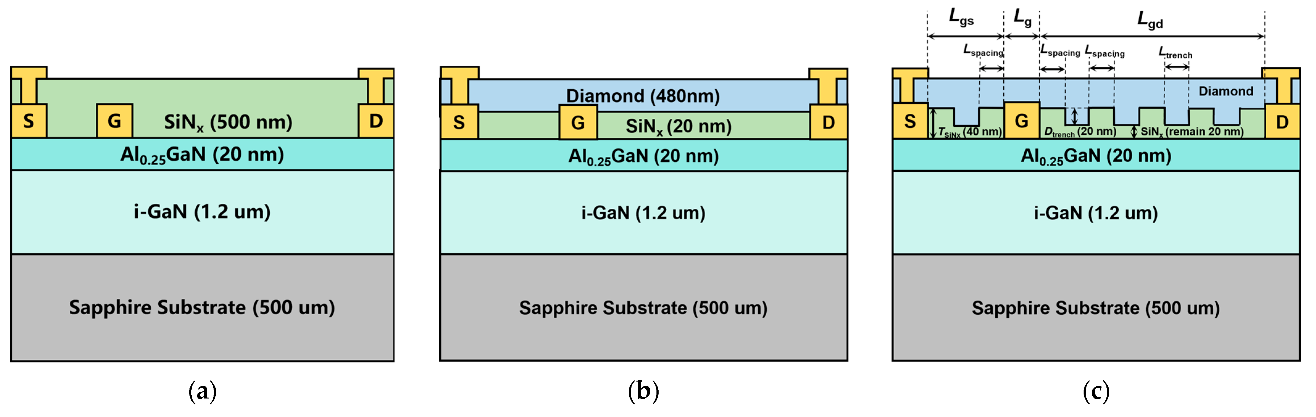
2. Device Structure Design and Simulation Setup

The schematics of SP, DP and TDP devices implemented for TCAD simulations are shown in Figure 1a–c. The AlGaN/GaN HEMTs consist of a 20 nm Al0.2Ga0.8N barrier layer with a 1.2 um i-GaN channel layer and a sapphire substrate. For SP, DP and TDP devices, the thickness of the passivation layer is 500 nm SiNx, 480/20 nm NCD/SiNx and 460/40 nm NCD/SiNx to control the total passivation layers’ thickness equally. For TDP, the depth, length and spacing of the trench are 20 nm, 100 nm and 100 nm, respectively. Therefore, the thickness of SiNx at the trench bottom is 20 nm, which can protect the barrier layer effectively during the NCD deposition process. The simulated device features a gate length (Lg) of 100 nm, a gate-source distance (Lgs) of 1.6 μm and a gate-drain distance (Lgd) of 2.4 μm.
In this simulation work, the semiconductor parameters of the GaN and AlGaN material were set up as shown in Table 1 according to the calibration results from the works of Karmalkar et al. [23]. The interface trap, located at 0.6 eV below the conduction band edge, was used. The areal density of the interface traps used in this work was 2 × 10¹²/cm2. The acceptor trap concentration in the buffer layer was 1 × 10¹⁸/cm2 at a trap energy location of 0.8 eV below the conduction band edge. The capture cross-sections for electrons and holes were 1 × 10⁻¹⁵/cm2 with a degeneracy factor of one. The models incorporated for the simulations were as follows: FERMI for the fermi statistic model; SRH for the carrier generation and recombination model; FLDMOB and ALBRCT to account for the mobility and saturation velocity effects; GANSAT for the nitride-specific mobility model; the IMPACT SELB impact ionization model for activating avalanche breakdown simulations; the trap model to configure the trap effects; and CALC.STRAIN to calculate the strain and the POLARIZATION model invoked for epitaxial strain due to the lattice mismatch and spontaneous polarization.
On account of the gate, AlGaN and GaN epilayers of SP, DP and TDP devices are the same simulated configurations; the energy band and electron concentration in the AlGaN/GaN heterojunction are conformed apparently. Figure 2 shows the conduction band energy and valence band energy vertically extracted from the gate to AlGaN and stopped in the GaN layer. The classic band diagram and electron distribution are displayed to verify the static electric characteristics in the GaN HEMT device model functioned reasonably. The peak electron concentrations at the interface of AlGaN and GaN are 1.58 × 10¹⁹/cm3.
Both NCD (10 W/cm-K) and SiNx (0.2 W/cm-K) are considered for device passivation layers. The thermal conductivity of AlGaN, GaN and sapphire substrate was set as 0.13, 1.8 and 0.35 W/cm-K [24]. The bottom of the structure was set to a fixed temperature of 300 K for SP, DP and TDP device simulations.

3. Results and Discussion

3.1. Junction Temperature Distributtion

The temperature distributions along the AlGaN/GaN heterojunction in SP, DP and TDP devices are shown in Figure 3a–c. It can be observed that the junction temperature of SP, DP and TDP devices increases as the bias increase from Vds/Vgs = 10 V/0 V to Vds/Vgs = 30 V/0 V. Furthermore, TDP devices exhibit the lowest average temperature biased at Vgs = 0 V and Vds = 10 V to 30 V compared to SP and DP devices. In particular, the peak junction temperature of TDP devices is 386.36 K biased at Vds/Vgs = 30 V/0 V, which is much lower than DP (404.58 K) and SP (447.59 K) devices. In Figure 3d,e, the cross-sectional lattice temperature profiles of SP, DP and TDP devices biased at Vds/Vgs = 30 V/0 V are presented with a normalized temperature scale bar. The trench structure combined the NCD and SiNx layers assist the horizontal heat dissipation so that the heat source region expands toward the gate-to-source access region. Therefore, TDP devices achieve better thermal management capability compared to conventional DP and SP devices.
According to the working principle of the AlGaN/GaN HEMT device, it is known that a higher current and power result in increased device temperature, which in turn leads to a greater probability of defects and easier degradation. As reported in previous research [25], every 25-kelvin degree junction temperature increases from 398 K to 448 K and the value of the mean time to failure of the GaN HEMTs decreases by an order of magnitude. Therefore, the TDP structure has been shown to significantly enhance the devices’ performance, along with improvements in reliability and lifetime.

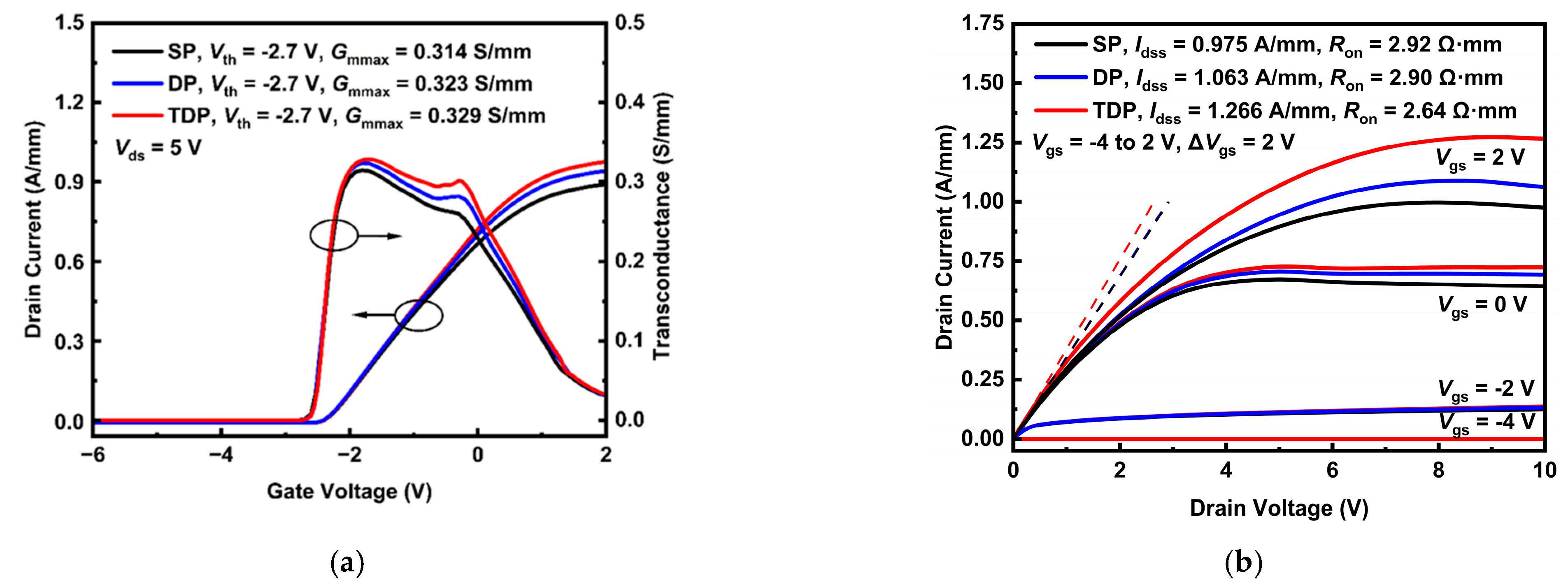
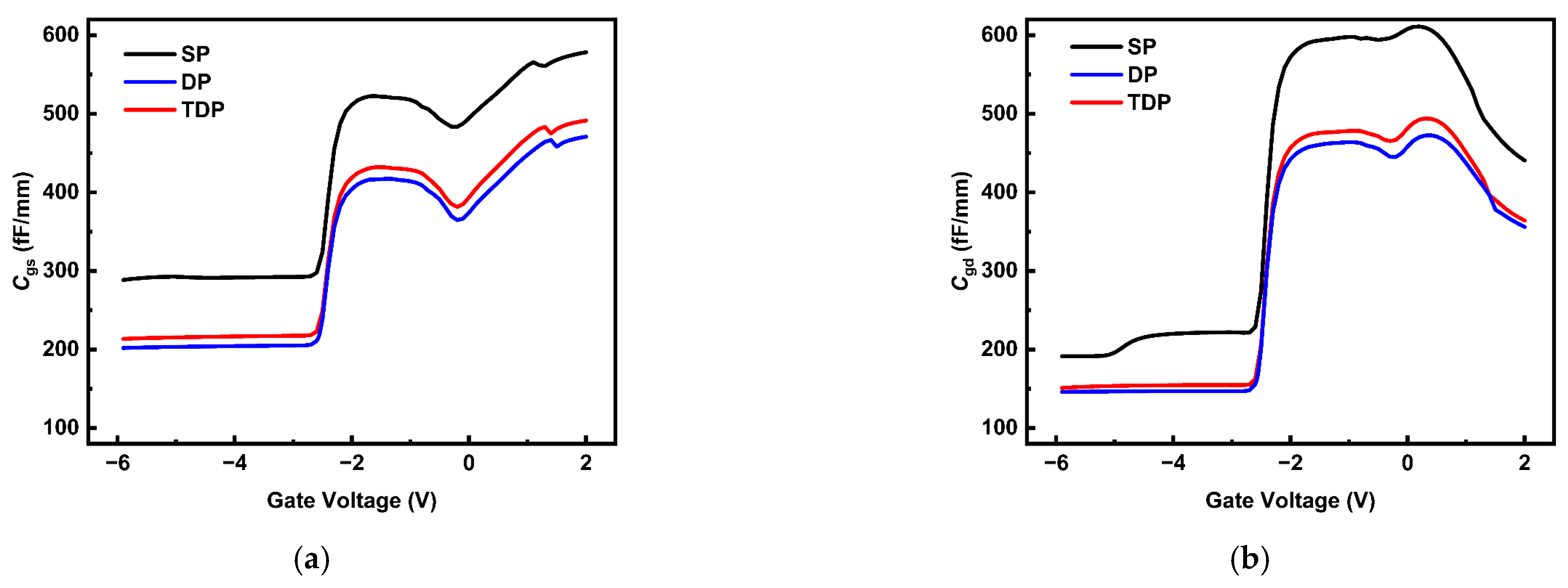
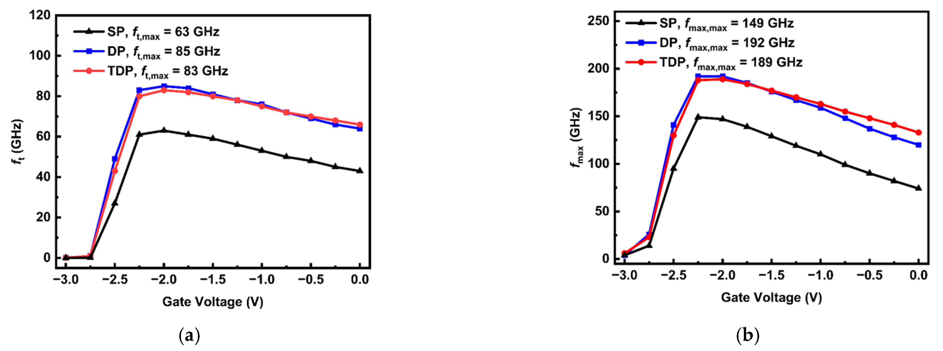
3.2. DC Characteristics and RF Small-Signal Characteristics

Figure 4a shows the typical DC transfer characteristics and transconductance curves of SP, DP and TDP devices. The results reveal that the threshold voltage of the devices is not impacted significantly by the SiNx and NCD structure. In addition, transconductance (Gm) of GaN HEMTs plays a critical role in device linearity and noise, which are important parameters in RF devices. According to the results, the maximum transconductance (Gmmax) is 0.329 S/mm for TDP devices, which is slightly higher than that of 0.314 S/mm and 0.323 S/mm for SP and DP devices.
The output characteristics of SP, DP and TDP devices are shown in Figure 4b. The output characteristics of SP and DP devices are degraded due to the severe self-heating effects. The self-heating phenomena occur in the saturation region of output characteristic and are improved significantly in the AlGaN/GaN HEMTs with TDP structure: as the Vgs increases, the improvement increases. TDP devices demonstrate the highest saturation drain current (Idss) of 1.266 A/mm and lowest conduction resistance (Ron) of 2.64 Ω·mm compared to Idss = 1.063 A/mm and 0.975 A/mm, Ron = 2.90 Ω·mm and 2.92 Ω·mm for DP and SP devices. These results indicate a 19.1% and 29.8% Idss improvement of TDP devices compared to DP and SP devices. The improvement in Idss for the TDP devices is attributed to the degradation of temperature-dependent mobility and 2DEG electron drift velocity.
The parasitic capacitances Cgs and Cgd as functions of Vgs (ranging from −6 V to 2 V) are shown in Figure 5. The higher parasitic capacitance observed in SP devices primarily arises from the larger relative permittivity of SiNx (~7 [26]) compared to NCD (~5.6 [27]). Replacing portions of SiNx with NCD in DP and TDP devices reduces the effective permittivity, thereby lowering their parasitic capacitances to different extents. Consequently, the SP device exhibits the highest effective permittivity and parasitic capacitance among the three structures. Additionally, the trench design in TDP devices results in a slightly larger volume of SiNx than in DP devices, leading to a marginally higher effective permittivity and parasitic capacitance in TDP compared to DP. This trade-off between parasitic capacitance and maximum transconductance explains why the TDP device’s peak fT and fmax values are slightly lower than those of the DP device. Nevertheless, the TDP structure maintains superior linearity. Importantly, the NCD/SiNx passivation significantly suppresses parasitic capacitance overall, directly influencing the frequency-dependent performance trends discussed in subsequent sections.
The typical small-signal characteristics ft and fmax related to the gate voltage for the SP, DP and TDP devices are presented in Figure 6. The cut-off frequency (ft) value is extracted by extrapolating the |H21|2 parameter, where the slope is −20 dB/dec and the gain reaches 0 dB. The maximum oscillation frequency fmax value is extracted from the unilateral power gain, where the slope is −20 dB/dec and the gain reaches 0 dB. Compared to the SP device, the DP and TDP devices exhibit higher ft and fmax as Vgs varying from −3 V to 0 V.
The maximum ft and fmax for the TDP device are slightly lower than those of the DP device. However, the TDP device demonstrates higher linearity due to its transconductance distribution being flatter than the DP device. Furthermore, the passivation layer materials function to introduce parasitic capacitances among all the electrodes, which in turn limit the device performance, resulting in lower ft and fmax max values. This effect is particularly significant in mm-wave devices, where the Lg and Lsd are shorter, ft and fmax are considerably sensitive to the parasitic capacitances (i.e., Cgs and Cgd). The equations for ft and fmax are Equations (1) and (2) [28]:
f t = g m 2 π C g s + C g d  
f m a x = f t 2 R i + R s + R g R d s + 2 π f t R g C g d  

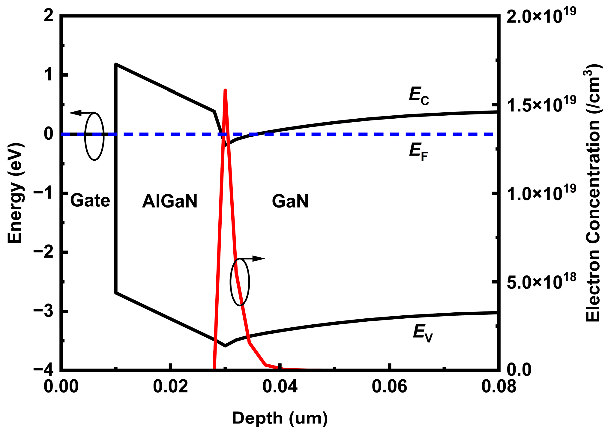
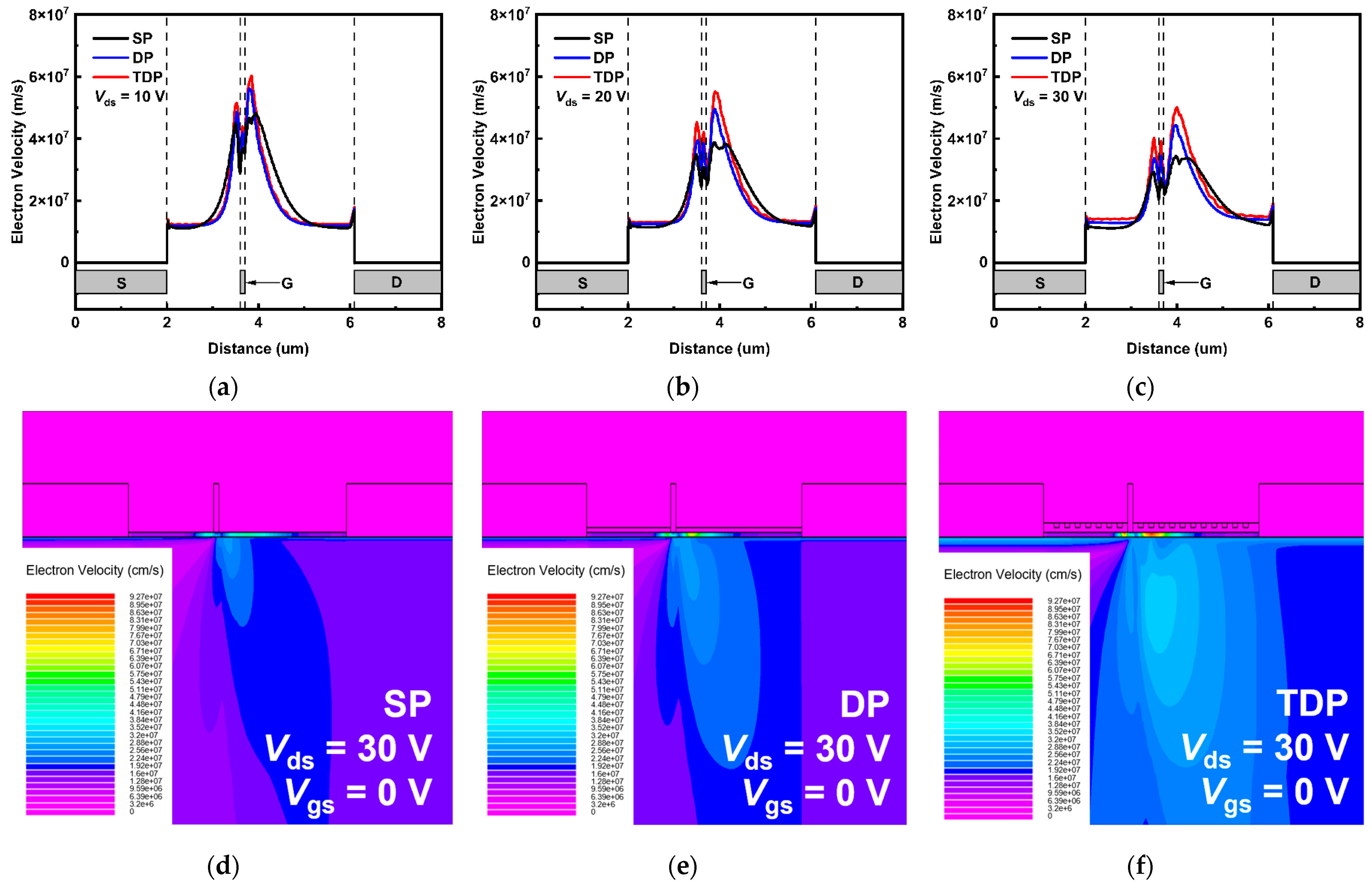
3.3. Electron Mobility and Electron Drift Velocity Distributtion

As a parameter strongly dependent on both temperature and electric field, electron mobility decreases with increasing temperature and electric field due to the increased optical phonon scattering [29]. In Figure 7, the SP, DP and TDP devices biased at Vds/Vgs = 10 V/0 V, 20 V/0 V, 30 V/0 V are shown. It is observed that the channel under the gate electrode exhibits the lowest electron mobility compared to the channel between the gate and the source/drain. This is because the electric field and lattice temperature peaks are located at the drain-side channel under the gate.
In Figure 7a–c, and as shown in Figure 3a–c, it is evident that under the same Vds bias condition, the average channel temperature of the TDP device is lower compared to DP and SP devices. Therefore, according to the compensation mobility model, the low-field mobility of the TDP device is higher than that of the DP and SP devices. The low-field mobility model used in this simulation is as follows [30]:
1 μ ( N , T L ) = a N I 10 17 c m 3 ln 1 + β C W 2 T 300   K 1.5 + b T 300   K 1.5 + c exp Θ T 1 ,  
where µ(N,TL) is the mobility as a function of total doping concentration (N) and lattice temperature (TL). Though AlGaN/GaN layers in SP, DP and TDP devices are defined as un-intended doping, GaN materials inherently exhibit an unintentional background doping concentration (1 × 10¹⁶/cm3) due to residual oxygen/silicon impurities during epitaxial growth [31]. Therefore, N equals to 1 × 10¹⁶/cm3 as the background doping concentration. Additionally, N I = 1 + k c N D ,   β C W 2 = 3.00 T 300   K 2 N I 10 17 c m 3 2 3 ,   Θ = ħ ω L O k B = 1065   K .   For parameters a = 2.61 × 10 4   V   s c m 2 ,   b = 2.90 × 10 4   V s c m 2 ,   c = 1.70 × 10 2   V s c m 2 .   Therefore, as the lattice temperature increases, the electron mobility along the channel will degrade. Moreover, as the Vds increases, electrons within the AlGaN/GaN HEMT devices channel acquire energy through the electric field generated by the bias voltage. Consequently, during their drift or diffusion motion, these electrons collide with the lattice, transferring energy to the lattice in the form of phonons. This process subsequently leads to an increase in the lattice temperature and a decrease in electron mobility.
Figure 7d–f illustrate the electron mobility distribution for SP, DP, and TDP devices under the same bias voltage conditions (Vds/Vgs = 30 V/0 V). With the high thermal conductivity layer NCD introduced, the total thermal conductivity of the passivation layer decreased efficiently. In addition, the trench structure coupled with NCD and SiNx layers can increase the contact area of the thermal interface so that the effective thermal resistance at the NCD/SiNx interface is reduced. As a result, it is evident that, due to the excellent heat dissipation effect of the TDP structure, the electron mobility in the two-dimensional plane of the TDP device is significantly higher than that of the DP and SP devices.
In Figure 8a–c, the electron drift velocity values along the channel of the devices biased at Vds/Vgs = 10 V/0 V, 20 V/0 V and 30 V/0 V are presented. The relationship between electron drift velocity and electron mobility can be described in terms of the influence of the electric field. Specifically, electron drift velocity refers to the average speed at which electrons move under the influence of an electric field, while electron mobility quantifies the drift velocity of electrons per unit electric field strength. This relationship can be mathematically expressed as follows [29]:
v d = μ E
where vd is electron drift velocity, µ is electron mobility and E is electric field. The electric field increases with higher Vds. Under the same Vds condition (i.e., the same E), vd is directly related to µ. Due to varying degrees of self-heating effects, the TDP device exhibits the highest µ compared to DP and SP devices. Consequently, it also possesses the highest vd along the channel. In low electric field conditions, this relationship remains linear, with vd increasing proportionally to the E. However, at high electric field intensities, the vd may approach saturation due to increased scattering events between electrons and the lattice, limiting the maximum achievable vd. As a result, with Vds increasing from 10 V to 30 V, all devices present the vd decrease. However, for any given Vds, the vd of the TDP device is always higher than that of the DP and SP devices, as shown in Figure 8d,e.

4. Conclusions

In this paper, AlGaN/GaN HEMTs with TDP layers are systematically studied using the TCAD Silvaco simulation tool. Compared to conventional SP devices and DP devices, TDP devices exhibit superior thermoelectric characteristics in mitigating self-heating effects. The peak junction temperature of TDP devices is 386.36 K biased at Vds/Vgs = 30 V/0 V, which is much lower than DP (404.58 K) and SP (447.59 K) devices. The simulations show that TDP devices exhibit higher electron mobility and drift velocity, which lead to a higher Idss of 1.266 A/mm, higher Gmmax of 0.329 S/mm and lower Ron of 2.64 Ω·mm than DP and SP devices because of better heat-dissipation capability. The TDP devices resolve the traditional trade-off between thermal dissipation and high-frequency operation in GaN HEMTs, making it particularly suitable for high-power-density and high-frequency applications. This capability holds great potential for enhancing the stability and reliability of the devices.

Author Contributions

Conceptualization, P.W.; methodology, P.W., C.D. and C.T.; software, P.W.; validation, C.D., C.T. and X.T.; formal analysis, P.W., N.T. and Q.W. (Qing Wang); investigation, P.W., C.D. and Q.W. (Qi Wang); resources, P.W.; data curation, P.W., C.D., W.T. and Z.W.; writing—original draft preparation, P.W.; writing—review and editing, Q.W. (Qing Wang) and H.Y.; visualization, Q.W. (Qing Wang) and H.Y.; supervision, Q.W. (Qing Wang) and H.Y.; project administration, Q.W. (Qing Wang) and H.Y.; funding acquisition, H.Y. All authors have read and agreed to the published version of the manuscript.

Funding

This work was supported by Fabrication of Normally-Off GaN Devices based on In situ SiNx Passivation and Selective Area Growth Recessed-Gate Techniques and the Reliability Study (National Natural Science Foundation of China, grant no.: 62274082), Research on mechanism of Source/Drain ohmic contact and the related GaN p-FET (grant no.: 2023A1515030034), Research on high-reliable GaN power device and the related industrial power system (grant no.: HZQB-KCZYZ-2021052), Study on the reliability of GaN power devices (grant no.: JCYJ20220818100605012), Research on novelty low-resistance Source/Drain ohmic contact for GaN p-FET (grant no.: JCYJ20220530115411025)), National Key R&D Program of China (2021YFB3600200), Guangdong Major Project of Basic and Applied Basic Research (2023B0303000012) and National Natural Science Foundation of China (62471011).

Data Availability Statement

The data that support the findings of this study are available from the corresponding authors upon reasonable request.

Conflicts of Interest

Nick Tao is currently employed at Maxscend Microelectronics Co., Ltd. and was employed by the company during the development of this manuscript. All contributions to this work and the manuscript were made independently, without any direction, guidance, or influence from the employer. Furthermore, no financial compensation was received from any source for Nick Tao’s contributions to this scientific work and manuscript. The remaining authors declare that the research was conducted in the absence of any commercial or financial relationships that could be construed as a potential conflict of interest.

References

  1. Ikeda, N.; Niiyama, Y.; Kambayashi, H.; Sato, Y.; Nomura, T.; Kato, S.; Yoshida, S. GaN power transistors on Si substrates for switching applications. Proc. IEEE 2010, 98, 1151–1161. [Google Scholar] [CrossRef]
  2. Heller, E.R.; Crespo, A. Electro-thermal modeling of multifinger AlGaN/GaN HEMT device operation including thermal substrate effects. Microelectron. Reliab. 2008, 48, 45–50. [Google Scholar] [CrossRef]
  3. Sozzi, G.; Menozzi, R. A review of the use of electro-thermal simulations for the analysis of heterostructure FETs. Microelectron. Reliab. 2007, 47, 65–73. [Google Scholar] [CrossRef]
  4. Hirama, K.; Taniyasu, Y.; Kasu, M. AlGaN/GaN high-electron mobility transistors with low thermal resistance grown on single-crystal diamond (111) substrates by metalorganic vapor-phase epitaxy. Appl. Phys. Lett. 2011, 98, 162112. [Google Scholar] [CrossRef]
  5. Ji, H.; Kuball, M.; Sarua, A.; Das, J.; Ruythooren, W.; Germain, M.; Borghs, G. Three-dimensional thermal analysis of a flip-chip mounted AlGaN/GaN HFET using confocal micro-Raman spectroscopy. IEEE Trans. Electron Devices 2006, 53, 2658–2661. [Google Scholar]
  6. Zhang, R.; Zhao, W.S.; Yin, W.Y.; Zhao, Z.G.; Zhou, H.J. Impacts of diamond heat spreader on the thermo-mechanical characteristics of high-power AlGaN/GaN HEMTs. Diam. Relat. Mater. 2015, 52, 25–31. [Google Scholar] [CrossRef]
  7. Tadjer, M.J.; Anderson, T.J.; Ancona, M.G.; Raad, P.E.; Komarov, P.; Bai, T.; Gallagher, J.C.; Koehler, A.D.; Goorsky, M.S.; Francis, D.A.; et al. GaN-on-diamond HEMT technology with TAVG= 176 C at PDC,max = 56 W/mm measured by transient thermoreflectance imaging. IEEE Electron Device Lett. 2019, 40, 881–884. [Google Scholar] [CrossRef]
  8. Ejeckam, F.; Francis, D.; Faili, F.; Twitchen, D.; Bolliger, B.; Babic, D.; Felbinger, J. S2-T1: GaN-on-diamond: A brief history. In Proceedings of the 2014 Lester Eastman Conference on High Performance Devices (LEC), Ithaca, NY, USA, 5–7 August 2014; IEEE: New York, NY, USA, 2014; pp. 1–5. [Google Scholar]
  9. Dussaigne, A.; Gonschorek, M.; Malinverni, M.; Py, M.A.; Martin, D.; Mouti, A.; Stadelmann, P.; Grandjean, N. High-mobility AlGaN/GaN two-dimensional electron gas heterostructure grown on (111) single crystal diamond substrate. Jpn. J. Appl. Phys. 2010, 49, 061001. [Google Scholar] [CrossRef]
  10. Tijent, F.Z.; Faqir, M.; Chouiyakh, H.; Essadiqi, E.H. integration methods of GaN and diamond for thermal management optimization. ECS J. Solid State Sci. Technol. 2021, 10, 074003. [Google Scholar] [CrossRef]
  11. Schwander, M.; Partes, K. A review of diamond synthesis by CVD processes. Diam. Relat. Mater. 2011, 20, 1287–1301. [Google Scholar] [CrossRef]
  12. Angus, J.C.; Will, H.A.; Stanko, W.S. Growth of diamond seed crystals by vapor deposition. J. Appl. Phys. 1968, 39, 2915–2922. [Google Scholar] [CrossRef]
  13. Arivazhagan, L.; Jarndal, A.; Nirmal, D. GaN HEMT on Si substrate with diamond heat spreader for high power applications. J. Comput. Electron. 2021, 20, 873–882. [Google Scholar] [CrossRef]
  14. Zhang, H.; Guo, Z.; Lu, Y. Enhancement of hot spot cooling by capped diamond layer deposition for multifinger AlGaN/GaN HEMTs. IEEE Trans. Electron Devices 2019, 67, 47–52. [Google Scholar] [CrossRef]
  15. Zhang, H.; Guo, Z. Thickness dependence and anisotropy of capped diamond thermal conductivity on cooling of pulse-operated GaN HEMTs. IEEE Trans. Compon. Packag. Manuf. Technol. 2021, 11, 233–240. [Google Scholar] [CrossRef]
  16. Zhou, Y.; Ramaneti, R.; Anaya, J.; Korneychuk, S.; Derluyn, J.; Sun, H.; Pomeroy, J.; Verbeeck, J.; Haenen, K.; Kuball, M. Thermal characterization of polycrystalline diamond thin film heat spreaders grown on GaN HEMTs. Appl. Phys. Lett. 2017, 111, 041901. [Google Scholar] [CrossRef]
  17. Wang, A.; Tadjer, M.J.; Anderson, T.J.; Baranyai, R.; Pomeroy, J.W.; Feygelson, T.I.; Hobart, K.D.; Pate, B.B.; Calle, F.; Kuball, M. Impact of intrinsic stress in diamond capping layers on the electrical behavior of AlGaN/GaN HEMTs. IEEE Trans. Electron Devices 2013, 60, 3149–3156. [Google Scholar] [CrossRef]
  18. Anderson, T.J.; Koehler, A.D.; Hobart, K.D.; Tadjer, M.J.; Feygelson, T.I.; Hite, J.K.; Pate, B.B.; Kub, F.J.; Eddy, C.R. Nanocrystalline Diamond-Gated AlGaN/GaN HEMT. IEEE Electron Device Lett. 2013, 34, 1382–1384. [Google Scholar] [CrossRef]
  19. Anderson, T.J.; Hobart, K.D.; Tadjer, M.J.; Koehler, A.D.; Imhoff, E.A.; Hite, J.K.; Feygelson, T.I.; Pate, B.B.; Eddy, C.R.; Kub, F.J. Nanocrystalline diamond integration with III-nitride HEMTs. ECS J. Solid State Sci. Technol. 2016, 6, Q3036. [Google Scholar] [CrossRef]
  20. Guggenheim, R.; Rothschild, J.A.; Rodes, L.; Hoffman, A. Thermal characteristics of diamond film coatings for GaN HEMT devices. In Proceedings of the 2015 IEEE International Conference on Microwaves, Communications, Antennas and Electronic Systems (COMCAS), Tel Aviv, Israel, 2–4 November 2015; IEEE: New York, NY, USA, 2015; pp. 1–3. [Google Scholar]
  21. Alomari, M.; Dipalo, M.; Rossi, S.; Diforte-Poisson, M.A.; Delage, S.; Carlin, J.F.; Grandjean, N.; Gaquiere, C.; Toth, L.; Pecz, B.; et al. Diamond overgrown InAlN/GaN HEMT. Diam. Relat. Mater. 2011, 20, 604–608. [Google Scholar] [CrossRef]
  22. Guo, H.; Li, Y.; Yu, X.; Zhou, J.; Kong, Y. Thermal performance improvement of AlGaN/GaN HEMTs using nanocrystalline diamond capping layers. Micromachines 2022, 13, 1486. [Google Scholar] [CrossRef]
  23. Karmalkar, S.; Mishra, U.K. Enhancement of breakdown voltage in AlGaN/GaN high electron mobility transistors using a field plate. IEEE Trans. Electron Devices 2001, 48, 1515–1521. [Google Scholar] [CrossRef]
  24. Zhang, Y.; Teo, K.H.; Palacios, T. Beyond thermal management: Incorporating p-diamond back-barriers and cap layers into AlGaN/GaN HEMTs. IEEE Trans. Electron Devices 2016, 63, 2340–2345. [Google Scholar] [CrossRef]
  25. Smith, K.V.; Haller, J.; Guerrero, J.; Smith, R.P.; Lal, R.; Wu, Y.F. Lifetime tests of 600-V GaN-on-Si power switches and HEMTs. Microelectron. Reliab. 2016, 58, 197–203. [Google Scholar] [CrossRef]
  26. Zhou, X.; Chen, Q.; Zhang, Q.M.; Zhang, S. Dielectric behavior of bilayer films of P(VDF-CTFE) and low temperature PECVD fabricated Si3N4. IEEE Trans. Dielectr. Electr. Insul. 2011, 18, 463–470. [Google Scholar] [CrossRef]
  27. Gao, X.-W.; Zhao, Z.-W.; He, Y.; Fan, S.-F.; Jiao, K.-R.; Lou, S.-Y.; Han, X.-Y.; Song, P.-F.; Cai, R.; Hu, Z.; et al. Nanodiamond: A promising metal-free nanoscale material in photocatalysis and electrocatalysis. Rare Met. 2024, 43, 3501–3552. [Google Scholar] [CrossRef]
  28. Bhat, A.M.; Shafi, N.; Sahu, C.; Periasamy, C. Analysis of AlGaN/GaN HEMT and its operational improvement using a grated gate field plate. J. Electron. Mater. 2021, 50, 6218–6227. [Google Scholar] [CrossRef]
  29. Neamen, D.A. Semiconductor Physics and Devices: Basic Principles, 4th ed.; McGraw-Hill: New York, NY, USA, 2012. [Google Scholar]
  30. ATLAS User’s Manual; Silvaco Int.: Santa Clara, CA, USA, 2010.
  31. Tan, L.T.; Chen, P.; Chua, S.J. Impact of V/III flux ratio and Si-doping concentration on GaN grown by metalorganic chemical-vapor deposition on sapphire substrate. In Proceedings of the ICONIP’02, the 9th International Conference on Neural Information Processing, Computational Intelligence for the E-Age (IEEE Cat. No. 02EX575), Penang, Malaysia, 19–21 December 2002; IEEE: New York, NY, USA, 2002; pp. 172–176. [Google Scholar]
Figure 1. Cross-sectional schematics of (a) SP, (b) DP and (c) TDP AlGaN/GaN HEMTs.
Nanomaterials 15 00574 g001
Figure 2. Band diagram and electron concentration distribution extracted from the gate to AlGaN and stopped at GaN layers.
Nanomaterials 15 00574 g002
Figure 3. Junction temperature distribution of the SP, DP and TDP AlGaN/GaN HEMTs biased at (a) Vds/Vgs = 10 V/0 V, (b) Vds/Vgs = 20 V/0 V and (c) Vds/Vgs = 30 V/0 V. For Vds/Vgs = 30 V/0 V, cross-sectional lattice temperature profiles of the (d) SP, (e) DP, and (f) TDP devices for Vds/Vgs = 30 V/0 V are presented.
Nanomaterials 15 00574 g003aNanomaterials 15 00574 g003b
Figure 4. (a) Transfer characteristics and (b) output characteristics of SP, DP and TDP AlGaN/GaN HEMTs.
Nanomaterials 15 00574 g004
Figure 5. (a) Cgs (b) Cgd related to gate voltage for SP, DP, TDP AlGaN/GaN HEMT devices.
Nanomaterials 15 00574 g005
Figure 6. (a) ft and (b) fmax related to gate voltage for SP, DP, TDP AlGaN/GaN HEMT devices.
Nanomaterials 15 00574 g006
Figure 7. Electron mobility of junctional region in the SP, DP and TDP AlGaN/GaN HEMTs biased at (a) Vds/Vgs = 10 V/0 V, (b) Vds/Vgs = 20 V/0 V and (c) Vds/Vgs = 30 V/0 V. For Vds = 30 V, cross-sectional electron mobility distributions of the (d) SP, (e) DP, and (f) TDP AlGaN/GaN HEMTs are presented.
Nanomaterials 15 00574 g007
Figure 8. Electron drift velocity of junctional region in the SP, DP and TDP AlGaN/GaN HEMTs biased at (a) Vds/Vgs = 10 V/0 V, (b) Vds/Vgs = 20 V/0 V and (c) Vds/Vgs = 30 V/0 V. For Vds = 30 V, cross-sectional electron velocity distributions of the (d) SP, (e) DP, and (f) TDP AlGaN/GaN HEMTs are presented.
Nanomaterials 15 00574 g008
Table 1. Calibration semiconductor parameters for GaN and AlGaN.
ParametersGaNAlGaN
Eg300 (eV)3.43.96
Affinity (eV)-3.82
Align0.80.8
Permittivity9.59.5
Mun (cm2/V-s)900600
Mup (cm2/V-s)1010
Vsatn (cm/s)2 × 107-
Nc300 (/cm3)1.07 × 10182.07 × 1018
Nv300 (/cm3)1.16 × 10181.16 × 1018
Disclaimer/Publisher’s Note: The statements, opinions and data contained in all publications are solely those of the individual author(s) and contributor(s) and not of MDPI and/or the editor(s). MDPI and/or the editor(s) disclaim responsibility for any injury to people or property resulting from any ideas, methods, instructions or products referred to in the content.

