Article

Photoelectrochemical Water Splitting by SnO2/CuO Thin Film Heterostructure-Based Photocatalysts for Hydrogen Generation

1
Department of Physics, University of Management and Technology, Lahore 54770, Pakistan
2
Center for Theoretical Physics, Khazar University, 41 Mehseti Str., Baku AZ1096, Azerbaijan
3
Department of Mathematics, Technical University of Cluj-Napoca, 400114 Cluj-Napoca, Romania
*
Author to whom correspondence should be addressed.
Nanomaterials 2025, 15(22), 1748; https://doi.org/10.3390/nano15221748
Submission received: 15 October 2025 / Revised: 6 November 2025 / Accepted: 14 November 2025 / Published: 20 November 2025
(This article belongs to the Section Energy and Catalysis)

Abstract

The emission of greenhouse gases from fossil fuels creates devastating effects on Earth’s atmosphere. Therefore, a clean energy source is required to fulfill the energy demand. Hydrogen is considered an energy vector, and the production of green hydrogen is a promising approach. Photoelectrochemical (PEC) water splitting is the best approach to produced green hydrogen, but the efficiency is low. To produce hydrogen by PEC splitting water, semiconductor photocatalysts have received an enormous amount of academic research in recent years. A new class of co-catalysts based on transition metals has emerged as a powerful tool for reducing charge transfer barriers and enhancing photoelectrochemical (PEC) efficiency. In this study, copper oxide (CuO) and tin oxide ( S n O 2 ) multilayer thin films were prepared by thermal evaporation to create an energy gradient between S n O 2 and CuO semiconductors for better charge transfer. To improve the crystallinity and reduce the defects, the prepared films were annealed in a tube furnace at 400 °C, 500 °C, and 600 °C in an argon inert gas environment. XRD results showed that S n O 2 /CuO-600 °C exhibited strong peaks, indicating the transformation from amorphous to polycrystalline. SEM images showed the transformation of smooth dense film to a granular structure by annealing, which is better for charge transfer from electrode to electrolyte. Optical properties showed that the bandgap was decreased by annealing, which might be diffusion of Cu and Sn atoms at the interface. PEC results showed that the S n O 2 /CuO-600 °C heterostructure exhibits the solar light-to-hydrogen (STH%) conversion efficiency of 0.25%.

1. Introduction

The world now strongly demands sustainable energy solutions because fossil fuel depletion, together with greenhouse gas emissions, damages our environment [1]. Solar energy and wind power, together with hydro generation, serve as sustainable power alternatives that are endlessly renewable. Solar energy represents a prominent choice because it exists widely, and it serves as a molecular basis for water splitting operations to produce hydrogen [2,3]. The energy carrier status of hydrogen presents an impressive opportunity to change existing global energy systems because it offers clean, renewable energy capabilities. The fuel serves as an attractive replacement for fossil fuels because of its concentrated energy content while releasing no greenhouse gases [4]. Photoelectrochemical (PEC) water splitting stands as one of the most efficient renewable methods among all hydrogen production techniques [5,6]. The water splitting reaction into hydrogen and oxygen takes place through solar irradiation by using semiconductor-based photocatalysts [5,7].
Advancements continue in hydrogen storage, together with transportation systems and use technologies, which point toward promising future development of hydrogen energy [8]. Governments across the globe spend money on hydrogen network development to establish a hydrogen-based economic system [9,10]. Green hydrogen production through water electrolysis operated by renewable energy sources will establish itself as a fundamental element for industry decarbonization and power generation and transportation systems decarbonization [11]. Researchers encounter obstacles in commercialization because of high production expenses, together with scarce efficient photocatalysts, along with stabilization issues. Research activities specifically work on finding affordable materials that boost hydrogen production speed and efficiency [12]. The breakthrough discovery of PEC water splitting with T i O 2 occurred when Faraji et al. (2019) introduced their method, which has initiated research to find different semiconductor materials [13]. The photoelectrochemical performance of W O 3 , F e 2 O 3 , and C u 2 O transition metal oxides has been shown to improve through their abilities to absorb visible wavelengths and promote electrical charge flow [14]. S n O 2 shows that this material demonstrates both high electron mobility and stable performance, which makes it very suitable for use as a photoanode. The big bandgap prevents this semiconductor from absorbing visible light photons [15,16]. CuO shows achievement as a photocathode material in research because it effectively absorbs visible light through its narrow bandgap [17]. The investigations of semiconductor photocatalysts represent a key approach for advancing photoelectrochemical water splitting through research. The efficiency of the PEC water splitting process can be enhanced by modifying the properties of semiconductor photocatalysts, i.e, by creating energy gradient for better charge transfer for making heterostructures, having better change transfer between electrode and electrolyte by nanostructuring and enhance the solar light absorption by modulating the bandgap of the semiconductor [18,19,20].
Tin oxide ( S n O 2 ) is an n-type semiconductor, has a large bandgap (3.6 eV), and shows remarkable chemical durability, but because of the large bandgap, most of the solar light passes through the material and is unable to produce electron-hole pairs [21]. CuO is a p-type semiconductor and has a narrow bandgap in the range of 1.2 eV to 1.6 eV [22]. Therefore, CuO is the best candidate for solar light absorption, but its valence band above the oxidation level of water becomes a bottleneck for the water splitting reaction [23].
Several studies have reported that combining n-type S n O 2 with p-type C u O forms a type-II heterojunction that enhances charge separation, suppresses recombination, and broadens light absorption into the visible range, thereby improving photocatalytic and photoelectrochemical (PEC) performance. Selleswari et al. (2019) demonstrated that C u O S n O 2 heterostructures exhibit superior UV light-driven photocatalytic activity owing to efficient electron–hole separation across the interface [24]. Animasahun et al. (2021) synthesized multilayered S n O 2 / C u O / S n O 2 thin films and observed improved photo absorption and reduced recombination losses compared with pristine oxides [25]. More recently, Salmanizadeh et al. (2024) reported that S n O 2 - C u O heterostructured photocatalysts synthesized via a simple solution process showed enhanced electron mobility and visible-light-driven PEC efficiency [26]. However, most of these studies employed sol-gel or hydrothermal techniques, which often result in non-uniform interfaces and limited crystallinity.
In this study, S n O 2 / C u O thin-film-based heterostructures are formed by thermal evaporation and then annealed at 400 °C, 500 °C, and 600 °C. The formation of heterostructures will create an energy gradient, which helps to separate the generated charge carriers efferently, which will reduce the combination rate, and it will also resolve the issue of oxidation of water because the valence band edge of S n O 2 is below the oxidation level of water. The annealing will definitely remove the defects in the structures and improve the crystallinity, which enables further better charge separation and reduces the recombination rate. As a result, the photocurrent response and solar light-to-hydrogen efficiency will be enhanced.

2. Experimental Procedure

S n O 2 /CuO heterostructures are formed by deposition of the CuO thin film followed by S n O 2 thin film by thermal evaporation. For this purpose, S n O 2 and CuO powders (Sigma Aldrich, St. Louis, MO, USA 99%>purity) were used as precursor materials. First of all, CuO powder of 1 g is placed in a tungsten boat in the thermal evaporation chamber, and the cleaned glass substrates and ITO substrates are placed in the substrate holder. When the vacuum of the chamber is 4 × 10 5 mbar, then 60 A current flows through the tungsten boat for resistive heating, and CuO powder is ablated and deposited on the glass substrates and ITO substrates. Similarly, then S n O 2 powder of 1 g is placed in a tungsten boat and again when the vacuum of the chamber is 4 × 10 5 mbar then 90 A current is passed through the tungsten boat to evaporate the S n O 2 powder. After 10 min of deposition, the S n O 2 film is deposited on the already-deposited CuO film; therefore, S n O 2 /CuO heterostructures are formed. The deposition of CuO and S n O 2 thin films is illustrated in Figure 1.
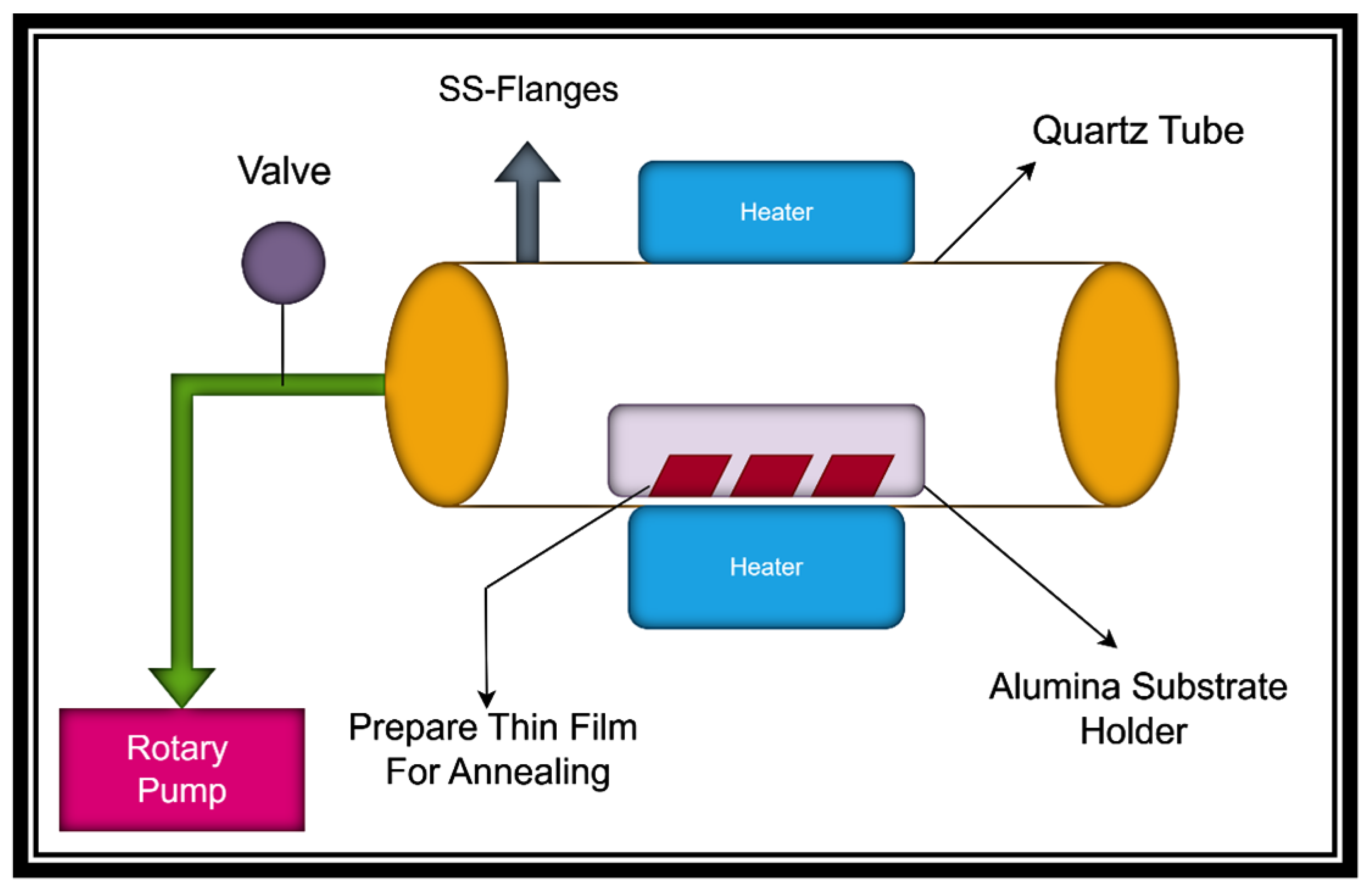
After that, the prepared samples are annealed at 400 °C, 500 °C, and 600 °C in a tube furnace for 2 h in the presence of argon gas (99.9% purity) at a flow rate of 100 sccm. The temperature rise rate is set to 7 °C/min for heating and cooling. The annealing of S n O 2 /CuO thin films in an argon environment is shown in Figure 2.
X-ray diffraction (XRD) analysis determined the structural properties of the synthesized thin films. A Bruker (AXS GmbH, Karlsruhe, Germany) D2-Phaser X-ray diffractometer was used for carrying out the measurements. XRD acquisition settings: Cu K α radiation, 2 θ range 20–80°, step size 0.02°. Scanning Electron Microscopy (SEM) was used to measure the morphological properties of the prepared sample. Optical properties were measured by spectrophotometry. Photoelectrochemical properties were measured by using a Gamry potentiostat (Gamry Instruments, Reference 3000, Warminster, PA, USA) setup in a three-electrode cell. The setup involves using a reference electrode made of Ag/AgCl, a counter electrode made of platinum wire, and a working electrode made of prepared samples. A concentration of 0.5 M N a 2 S O 4 is used as the electrolyte. The linear sweep voltametry of samples was measured under dark and light conditions (100 mW.cm−2).

3. Results and Discussion

3.1. Structural Analysis

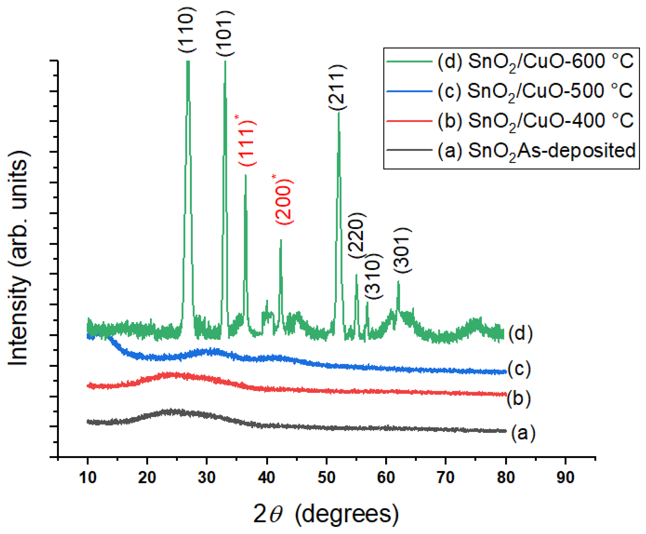
XRD patterns of as-deposited S n O 2 thin film and S n O 2 /CuO-400 °C, S n O 2 /CuO-500 °C, and S n O 2 /CuO-600 °C thin films are shown in Figure 3. It was observed that as-deposited S n O 2 thin film, S n O 2 /CuO-400 °C and S n O 2 /CuO-500 °C are amorphous, while the S n O 2 /CuO-600 °C thin film showed strong peaks, which indicates it is polycrystalline. It was noticed that peaks present at 2 θ = 26.78°, 32.96°, 52.04°, 54.94°, 56.68°, 61.92° with corresponding reflection planes (110), (101), (211), (220), (310) of S n O 2 that are well matched with JCPDS card no. 41-1049 [27]. Similarly, peaks appeared at 2 θ = 36.37°, 42.24° with the corresponding reflection planes (111)* and (200)* belonging to CuO. The peaks of CuO belong to a face-centered cubic crystal structure with the JCPDS card number 05-0667 [28]. The transformation from amorphous to crystalline indicates the arrangement of atoms and a decrease in defects, which enhances the charge carrier separation rate and decreases the recombination rates, which increases photocurrent response [29].

3.2. Morphological Analysis

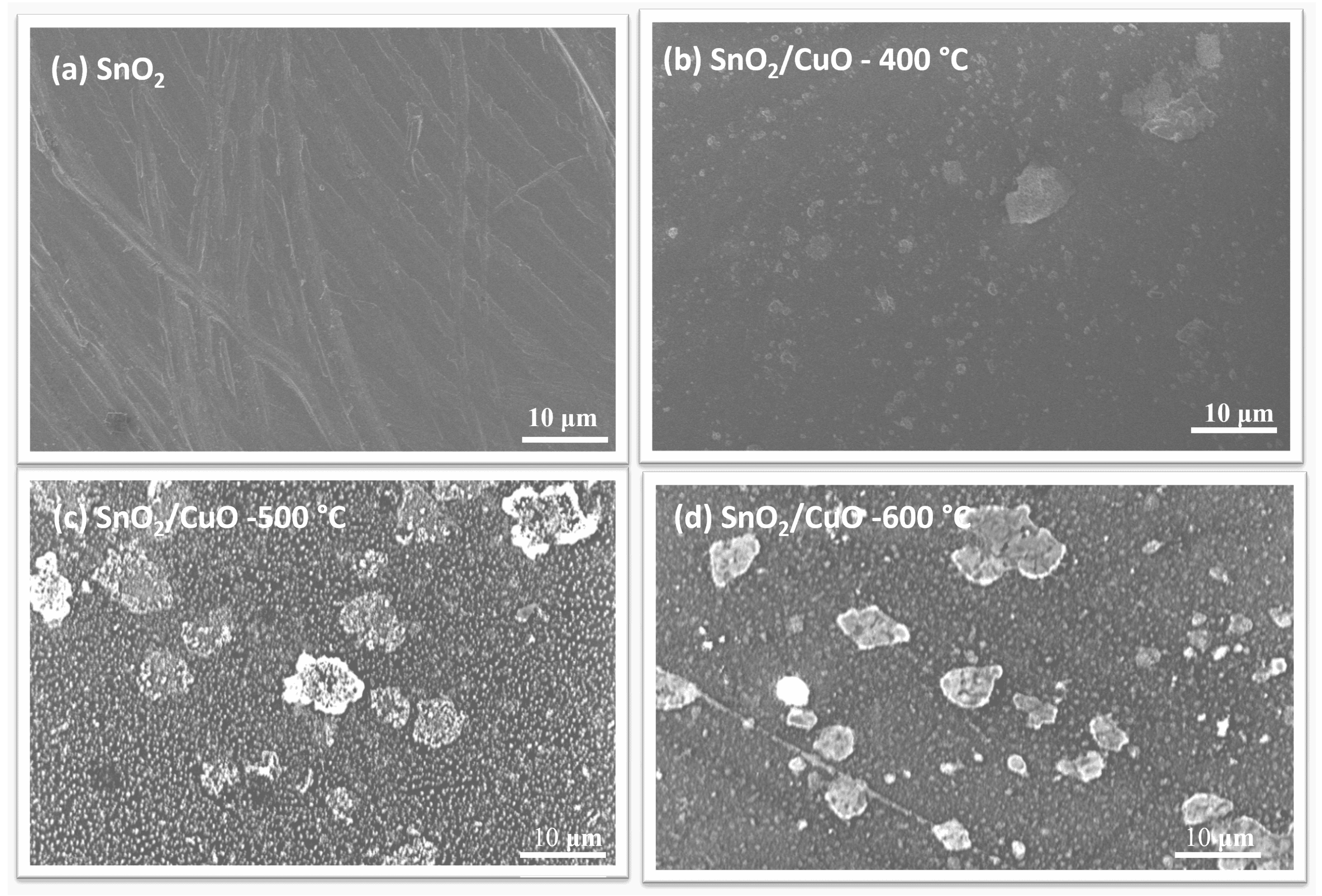
Scanning Electron Microscopy (SEM) was used to analyze the surface morphology of S n O 2 and S n O 2 /CuO thin films annealed at 400 °C, 500 °C, and 600 °C temperatures. Figure 4a is the as-deposited S n O 2 thin film, which reveals a smooth and dense surface with fine structural characteristics, indicating uniform and compact film formation. The S n O 2 /CuO-400 °C thin film in Figure 4b exhibits tiny, distributed grains on the surface, indicating the start of development of the CuO phase and the establishment of a heterostructure interface. As the annealing temperature reached 500 °C Figure 4c, the film formed a granular shape with visible spherical and irregularly shaped particles, suggesting increased grain formation. At 600 °C, shown in Figure 4d, the S n O 2 /CuO heterostructure showed bigger, well-defined grains with clear borders, indicating considerable grain development by thermal energy-driven diffusion. The formation of grains by increasing annealing temperature is suitable for charge transfer between the electrode and electrolyte resulting in an increase in photocurrent response [30].

3.3. Bandgap Determination

The optical properties of the prepared films were measured by a spectrophotometer. The spectrometry of the prepared samples is based on the Beer-Lambert principle
I = I 0 e α x
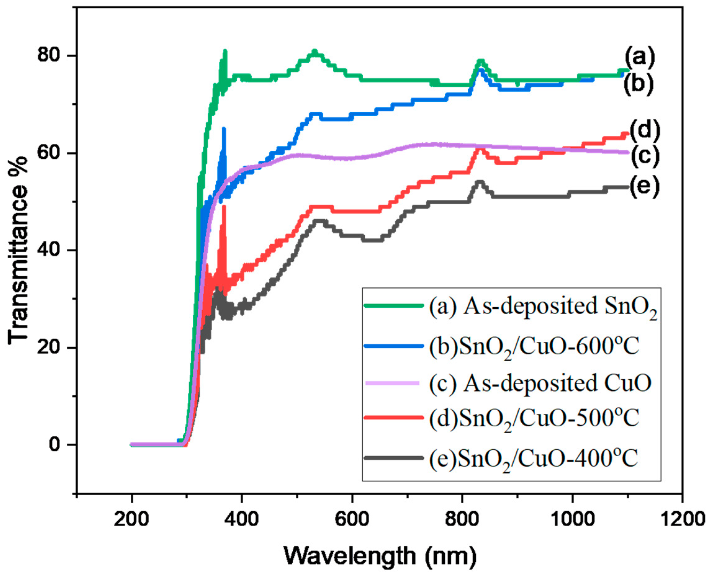
Here, I 0 represents the incident light intensity, I represents the transmittance light intensity, α represents the absorption coefficient, and x represents the film thickness. The transmittance spectra of the prepared samples are shown in Figure 5.
Figure 5 represents the transmittance of S n O 2 and S n O 2 /CuO thin film annealed at 400 °C, 500 °C, and 600 °C. It was noticed that all thin films are transparent in the visible region (380 to 760 nm). The transmittance of S n O 2 /CuO-600 °C heterostructure thin film was increased by increasing the temperature. It is due to the decrease in defects and arrangements of atoms that allow light to pass through the sample [31]. The estimated average transmittance in the visible region is 75%. The following formula can be used to determine the absorption constant a.
a = 1 d l n 1 T f
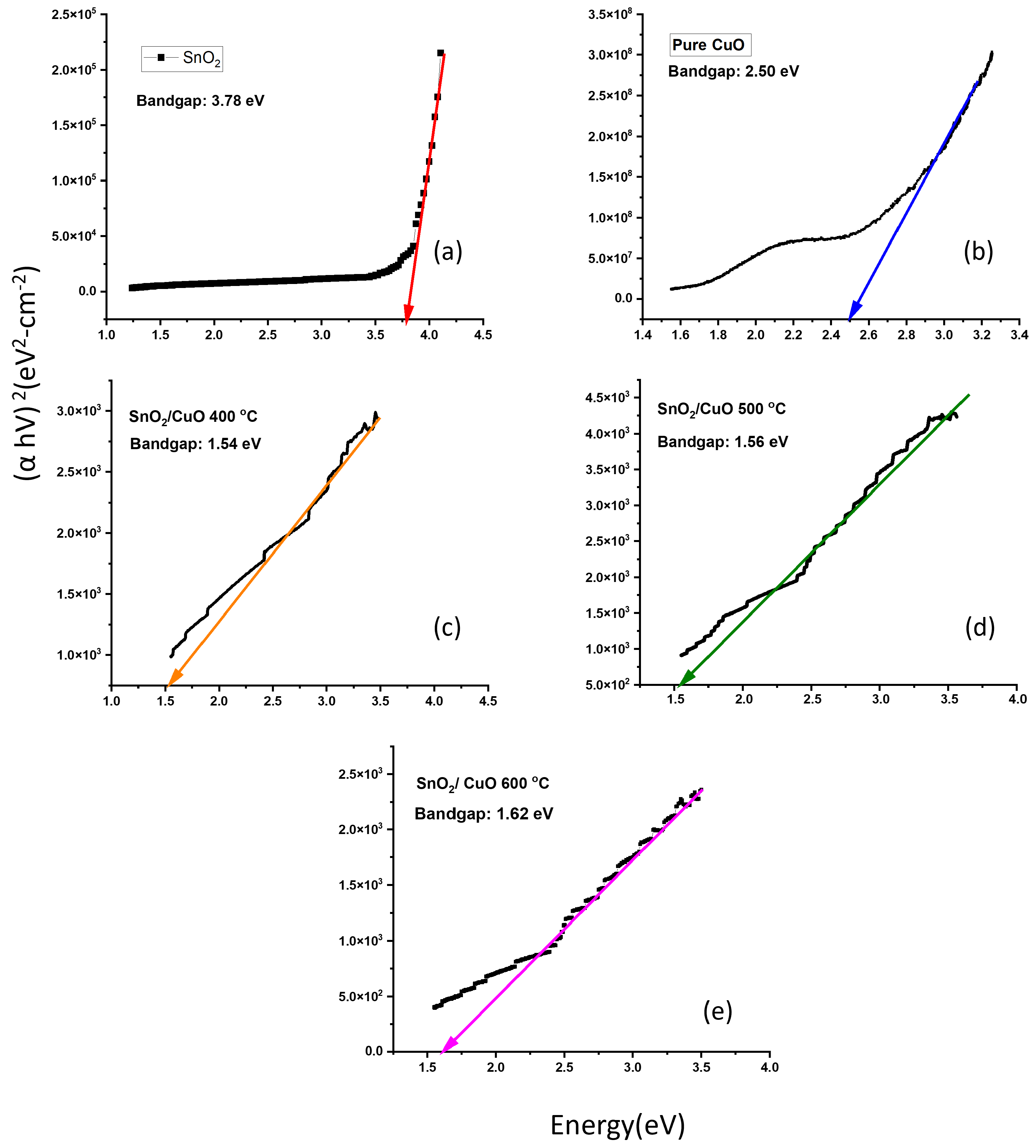
The thickness of the thin film is denoted by d, and the transmittance of the thin film is denoted by T f . In the strong absorption region, the absorption coefficient is dependent on the incident photon energy (E). Tauc was the one who first proposed utilizing optical absorbance to determine the semiconductor bandgap ( E g ). A Tauc plot method helped determine the optical band gap of all prepared thin films. The optical bandgap measurement of unprocessed S n O 2 thin film deposited onto Si (100) substrate presented a value of 3.78 eV (Figure 6a) that is well matched with the already reported values [32]. The as-deposited CuO thin film exhibited an optical band gap of 2.50 eV, as extracted from the Tauc-plot analysis (Figure 6b). The relatively high value of the band gap compared to typical values for bulk CuO suggests that the film is not purely CuO but rather contains a mixture of C u 2 O and CuO phases. The presence of C u 2 O , (which has a higher bandgap than CuO) shifts the effective optical absorption edge upward, and thus the measured value of 2.50 eV is consistent with the literature for mixed C u 2 O /CuO phases [33]. The Tauc plot analysis revealed the bandgap values of S n O 2 /CuO-400 °C as 1.54 eV, S n O 2 /CuO-500 °C as 1.56 eV, and S n O 2 /CuO-600 °C as 1.62 eV in that order. The reduction in the heterostructure thin films’ bandgap below pure S n O 2 and CuO occurs due to interface diffusion of Cu atoms and Sn atoms, which act as dopants and create dopant defect levels within the bandgap [34]. The S n O 2 / C u O heterostructures fabricated by thermal evaporation in this work exhibit optical bandgap values between 1.54 eV and 1.62 eV, which are slightly lower than those reported for sol-gel or hydrothermally prepared heterostructures typically 1.65–1.80 eV [35]. This reduction indicates improved interfacial coupling and band alignment due to controlled annealing and film uniformity.

3.4. Photoelectrochemical Water Splitting

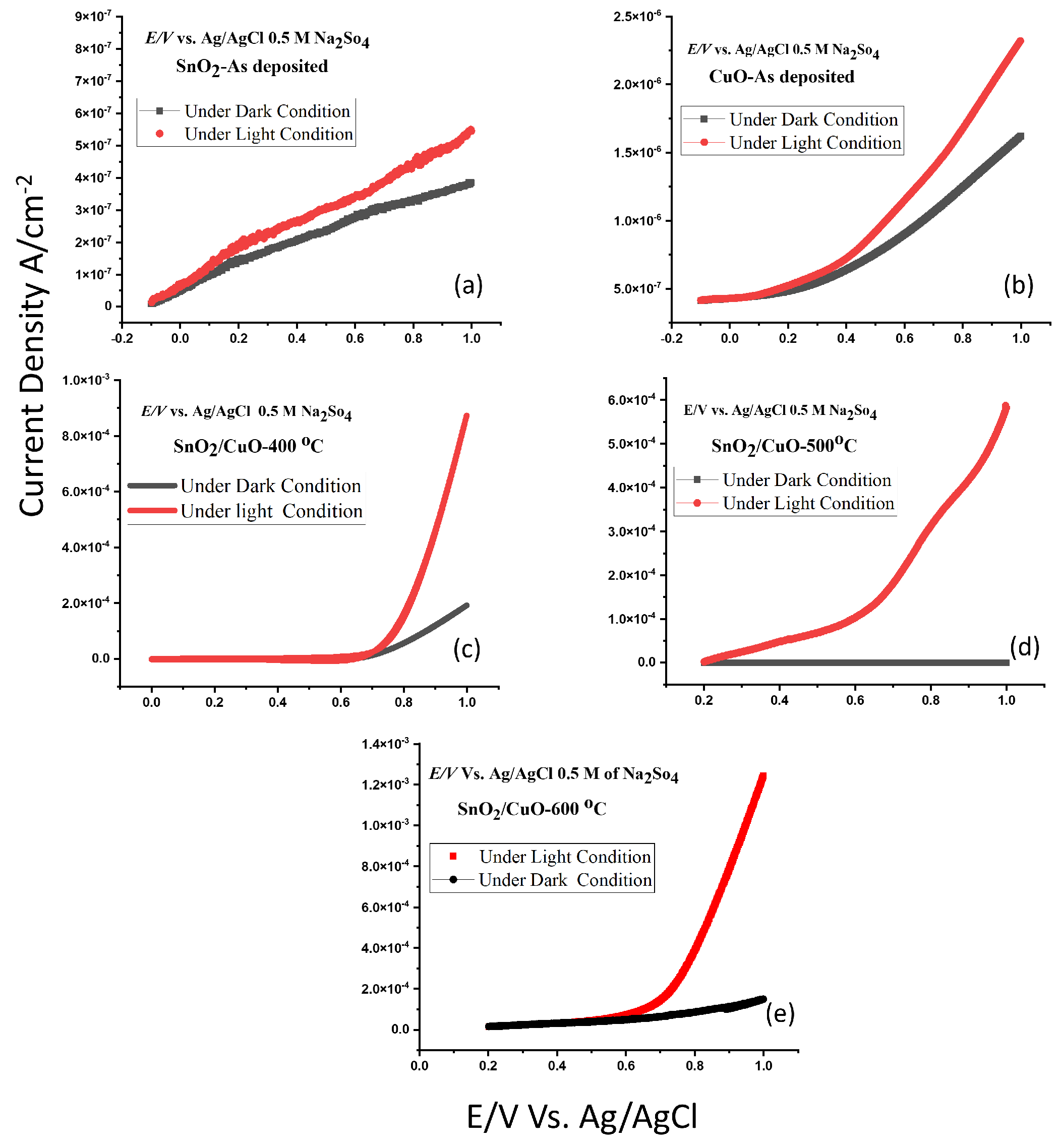
The photoelectrochemical properties of the as-deposited S n O 2 , as-deposited CuO, S n O 2 / C u O -400 °C, S n O 2 / C u O -500 °C, and S n O 2 / C u O -600 °C were measured by measuring the linear sweep voltammetry under dark conduction and under light conditions to estimate the photocurrent response. LSV results showed that the photocurrent density of pure tin oxide and copper oxide is small and was increased when S n O 2 / C u O heterostructure is formed. It is due to the creation of an energy gradient that enhances the charge separation, and this phenomenon is illustrated in Figure 7, which explains the plausible reaction mechanism of oxidation and reduction reactions of water splitting.
It was also noticed that the photocurrent response was increasing in the S n O 2 / C u O heterostructure by increasing the annealing temperature. The increase in photocurrent was due to the decrease in defects in the films, which results in a decrease in recombination rate and better charge separation and formation of granular structure by annealing, which if effective for better charge transfer between electrode and electrolyte results in an enhancement in reaction rate [36]. The solar light-to-hydrogen conversion efficiency (STH %) of the prepared samples was estimated according to the following Equation [19].
S T H % = ( 1.23 V b i a s ) × J p × 100 %
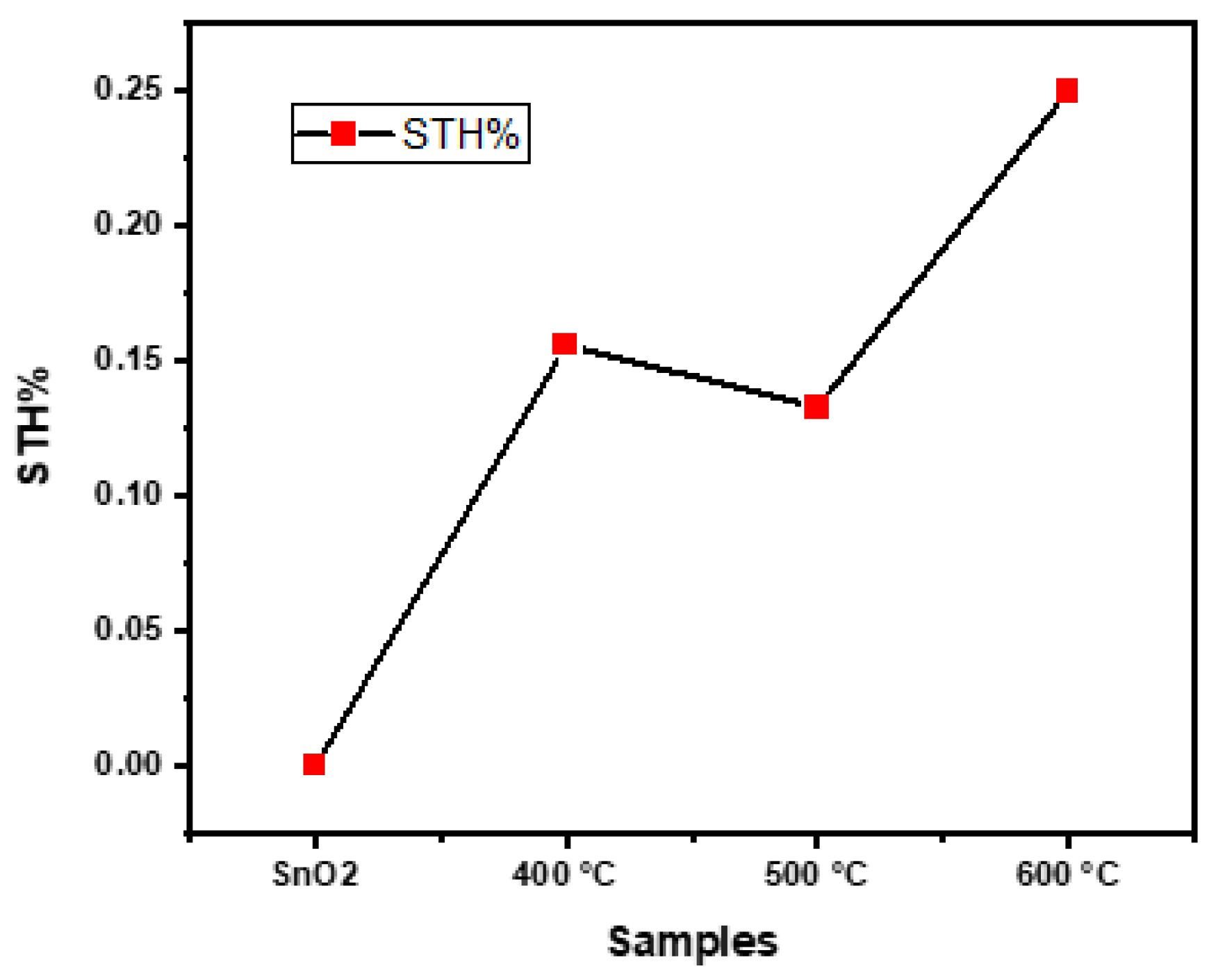
where P is the intensity of the solar spectrum, J is the photocurrent density, and V b i a s is the applied voltage. Table 1 has been updated to include typical reference materials such as T i O 2 , W O 3 , and C u 2 O for comparison. The obtained solar-to-hydrogen (STH %) conversion efficiencies of our thermally evaporated S n O 2 / C u O thin films are very good relative to the literature reports on similar metal oxide heterostructures. In our study, the photocurrent density and STH % of the S n O 2 / C u O heterostructures increased significantly compared with the pristine films. Although certain studies using sol-gel or hydrothermal routes have reported higher absolute STH values for more complex systems, the relative enhancement achieved in our work by forming a simple bilayer heterostructure is substantially larger. This clearly demonstrates the beneficial effect of controlled thermal evaporation, annealing crystallinity, and charge-transfer efficiency in S n O 2 / C u O systems.
It was noticed that S n O 2 / C u O -600 °C thin film showed STH% almost 1560 times more photocurrent response compared to pure C u O , which indicates that the formation of heterostructures enhances the hydrogen production and can be enhanced further by creating better-quality film and a better way to nanostructure them.
The value of photocurrent density under light conditions is where the value under dark conditions is obtained by applying a potential of 1 V (Figure 8). Similarly, the photocurrent response of S n O 2 / C u O -400 °C, S n O 2 / C u O -500 °C, S n O 2 / C u O -600 °C is measured and given in Table 1. It was noticed that the photocurrent response of the heterostructure is more compared to the pure C u O and S n O 2 thin films. It is due to the creation of an energy gradient and the increased light absorption of the samples. The photocurrent response of the heterostructure annealed at 600 °C is more compared to S n O 2 / C u O -400 °C and S n O 2 / C u O -500 °C. It is due to the motion of C u 2 O from C u O , which creates a better energy gradient for charge transformation. The S n O 2 / C u O heterostructures under 600 °C annealing temperature generated superior results in PEC measurements regarding their photocurrent density and hydrogen evolution efficiency. The photocurrent density obtained for the S n O 2 / C u O –600 °C sample (0.25 STH %) betters many comparable systems reported previously, where STH efficiencies generally remain below 0.15% under similar conditions. These results confirm that the optimized thermal evaporation route enhances carrier separation, crystallinity, and PEC performance, underscoring the novelty of our deposition method.
Figure 9 depicts a comparison of bare S n O 2 , C u O , and S n O 2 / C u O with a heterostructure.

4. Conclusions

The research investigation showed successful evidence that S n O 2 / C u O thin-film heterostructures deliver efficient PEC hydrogen generation capabilities. An improved photocatalytic effect and advanced light absorption, together with increased charge separation, result from combining S n O 2 and C u O . The S n O 2 / C u O heterostructures were prepared via a stepwise thermal evaporation process. The samples were annealed in an argon gas environment. Optical properties showed that pristine S n O 2 and C u O thin films showed good transmittance in the visible region, while heterostructure S n O 2 / C u O thin films showed less transmittance in the visible region because of the increase in light scattering at the interface. XRD data depict that as-deposited S n O 2 , heterostructure of S n O 2 / C u O of 400 °C and 500 °C showed an amorphous phase due to the presence of defects and less planes for a present to generate peaks, while the heterostructure S n O 2 / C u O films annealed at 600 °C are polycrystalline in nature, confirming improved grain growth and reduced lattice defects compared to lower-temperature samples. Tauc plots of the prepared samples showed that heterostructured S n O 2 / C u O thin films have a smaller bandgap (1.56 eV) compared to pure S n O 2 (3.78 eV) and CuO (2.50 eV), which is attributed to the diffusion of C u O in the S n O 2 thin films, leading to enhanced light absorption and charge transfer. Photoelectrochemical properties showed that heterostructure S n O 2 / C u O thin films showed better photocurrent response and solar-to-hydrogen conversion efficiency than pristine films. The highest efficiency 0.25% was achieved for S n O 2 / C u O -600 °C, showing the beneficial impact of optimal annealing temperatures on film performance. Annealing and enhanced manufacturing procedures can help to further optimize hydrogen production. Future research will focus on improving thin-film stability and investigating other metal oxide combinations to enhance hydrogen generation efficiency. Furthermore, nanostructuring and enhanced deposition processes are predicted to provide smoother coatings with better photoelectrochemical properties.

Author Contributions

Conceptualization, J.A.F., T.H., M.B., K.A. and L.-I.C.; methodology, J.A.F., T.H., M.B., K.A. and L.-I.C.; software, J.A.F., T.H., M.B., K.A. and L.-I.C.; validation, J.A.F., T.H., M.B., K.A. and L.-I.C.; formal analysis, J.A.F., T.H., M.B., K.A. and L.-I.C.; investigation, J.A.F., T.H., M.B., K.A. and L.-I.C.; resources, J.A.F., T.H., M.B., K.A. and L.-I.C.; data curation, J.A.F., T.H., M.B., K.A. and L.-I.C.; writing—original draft preparation, J.A.F., T.H., M.B., K.A. and L.-I.C.; writing—review and editing, J.A.F., T.H., M.B., K.A. and L.-I.C.; visualization, J.A.F., T.H., M.B., K.A. and L.-I.C.; supervision, J.A.F., T.H., M.B., K.A. and L.-I.C.; project administration, J.A.F., T.H., M.B., K.A. and L.-I.C.; funding acquisition, J.A.F., T.H., M.B., K.A. and L.-I.C. All authors have read and agreed to the published version of the manuscript.

Funding

This research received no external funding.

Data Availability Statement

Dataset available on request from the authors.

Conflicts of Interest

The authors declare no conflicts of interest.

References

  1. Wang, J.; Azam, W. Natural resource scarcity, fossil fuel energy consumption, and total greenhouse gas emissions in top emitting countries. Geo. Front. 2024, 15, 101757. [Google Scholar] [CrossRef]
  2. Luque-Urrutia, J.A.; Ortiz-García, T.; Solà, M.; Poater, A. Green energy by hydrogen production from water splitting, water oxidation catalysis and acceptorless dehydrogenative coupling. Inorganics 2023, 11, 88. [Google Scholar] [CrossRef]
  3. Dutta, T.; Chaturvedi, P.; Thakur, A.; Mishra, S.K. Review and Outlook of Graphene-Based Catalysis: Revolutionizing Water Splitting for Sustainable Hydrogen Production. Energy Fuels 2025, 39, 8827–8870. [Google Scholar] [CrossRef]
  4. Hassan, Q.; Algburi, S.; Sameen, A.Z.; Jaszczur, M.; Salman, H.M. Hydrogen as an energy carrier: Properties, storage methods, challenges, and future implications. Envir. Syst. Decis. 2024, 44, 327–350. [Google Scholar] [CrossRef]
  5. Vilanova, A.; Dias, P.; Lopes, T.; Mendes, A. The route for commercial photoelectrochemical water splitting: A review of large-area devices and key upscaling challenges. Chem. Soc. Rev. 2024, 53, 2388–2434. [Google Scholar] [CrossRef] [PubMed]
  6. Wang, G.; Chen, A.; Chen, Y.; Qiao, F.; Wang, J.; Yang, N.; Wen, Z. Advancements in electrochemical synthesis: Expanding from water electrolysis to dual-value-added products. EScience 2024, 5, 100333. [Google Scholar] [CrossRef]
  7. Peng, Y.; Rabeah, J.; Junge, H.; Beller, M. A Protocol for Unveiling the Nature of Photocatalytic Hydrogen Evolution Reactions: True Water Splitting or Sacrificial Reagent Acceptorless Dehydrogenation? Angew. Chem. Int. Ed. 2024, 63, e202408626. [Google Scholar] [CrossRef]
  8. Son, M.K. Key strategies on Cu2O photocathodes toward practical photoelectrochemical water splitting. Nanomaterials 2023, 13, 3142. [Google Scholar] [CrossRef]
  9. Sun, H.; Wang, Z.; Meng, Q.; White, S. Advancements in hydrogen storage technologies: Enhancing efficiency, safety, and economic viability for sustainable energy transition. Int. J. Hydrog. Energy 2025, 105, 10–22. [Google Scholar] [CrossRef]
  10. Dou, Y.; Sun, L.; Ren, J.; Dong, L. Opportunities and future challenges in hydrogen economy for sustainable development. Hydrogen Econ. 2023, 537–569. [Google Scholar]
  11. Shaban, M.; Almohammedi, A.; Saad, R.; Sayed, A.N.E. Design of SnO2: Ni, Ir nanoparticulate photoelectrodes for efficient photoelectrochemical water splitting. Nanomaterials 2022, 12, 453. [Google Scholar] [CrossRef] [PubMed]
  12. Alasali, F.; Abuashour, M.I.; Hammad, W.; Almomani, D.; Obeidat, A.M.; Holderbaum, W. A review of hydrogen production and storage materials for efficient integrated hydrogen energy systems. Energy Sci. Eng. 2024, 12, 1934–1968. [Google Scholar] [CrossRef]
  13. Faraji, M.; Yousefi, M.; Yousefzadeh, S.; Zirak, M.; Naseri, N.; Jeon, T.H.; Moshfegh, A.Z. Two-dimensional materials in semiconductor photoelectrocatalytic systems for water splitting. Ener. Environ. Sci. 2019, 12, 59–95. [Google Scholar] [CrossRef]
  14. Rizzi, G.A.; Girardi, L. Metal oxides for photoelectrochemical fuel production. In Tailored Functional Oxide Nanomaterials: From Design to Multi-Purpose Applications; John Wiley & Sons, Inc.: Hoboken, NJ, USA, 2022; pp. 339–377. [Google Scholar]
  15. Prasad, A.; Verma, J.; Suresh, S.; Arisutha, S. Recent advancements in the applicability of SnO2-based photo-catalysts for hydrogen production: Challenges and solutions. Waste Dispos. Sustain. Energy 2022, 4, 179–192. [Google Scholar] [CrossRef]
  16. Nassar, M.H.; El-Nowihy, G.H. CdS–SnO2–ZnO–Doped TiO2 Nanocomposite: A High-Efficiency Photoanode for Dye-Sensitized Solar Cells. ACS Appl. Energy Mater. 2025, 8, 16066–16074. [Google Scholar] [CrossRef]
  17. Uma, H.B.; Kumar, M.S.V.; Ananda, S. Semiconductor-assisted photodegradation of textile dye, photo-voltaic and antibacterial property of electrochemically synthesized Sr-doped CuO nano photocatalysts. J. Mol. Struct. 2022, 1264, 133110. [Google Scholar] [CrossRef]
  18. Liu, D.; Kuang, Y. Particle-based photoelectrodes for PEC water splitting: Concepts and perspectives. Adv. Mater. 2024, 36, 2311692. [Google Scholar] [CrossRef] [PubMed]
  19. Riffat, M.; Ali, H.; Qayyum, H.A.; Bilal, M.; Hussain, T. Enhanced solar-driven water splitting by ZnO/CdTe heterostructure thin films-based photocatalysts. Int. J. Hydrogen Energy 2023, 48, 22069–22078. [Google Scholar] [CrossRef]
  20. Islam, M.S.; Rahman, M.K.; Hossain, M.S.; Howlader, A.S.; Mim, J.J.; Islam, S.; Hossain, N. Advantages of Narrow Bandgap Nanoparticles in Semiconductor Development and their Applications. Semiconductors 2024, 58, 849–873. [Google Scholar] [CrossRef]
  21. Pinto, A.H.; Nogueira, A.E.; Dalmaschio, C.J.; Frigini, I.N.; de Almeida, J.C.; Ferrer, M.M.; de Mendonça, V.R. Doped tin dioxide (d-SnO2) and its nanostructures: Review of the theoretical aspects, photocatalytic and biomedical applications. Solids 2022, 3, 327–360. [Google Scholar] [CrossRef]
  22. Babu, M.H.; Podder, J.; Dev, B.C.; Sharmin, M. p to n-type transition with wide blue shift optical band gap of spray synthesized Cd doped CuO thin films for optoelectronic device applications. Surfaces Interfaces 2020, 19, 100459. [Google Scholar] [CrossRef]
  23. Zhang, Y.M.; Zhao, Z.Y.; Tang, W.; Feng, J.Y.; Zhang, J.; Liu, Q.J.; Zou, Z.G. CuCoO2/CuO heterostructure: Understanding the role of band alignment in selective catalysis for overall water splitting. J. Mater. Chem. A 2023, 11, 20151–20164. [Google Scholar] [CrossRef]
  24. Selleswari, D.; Meena, P.; Mangalaraj, D. Design of CuO/SnO2 heterojunction photocatalyst with enhanced UV light-driven photocatalytic activity on congo-red and malachite green dyes. J. Iran. Chem. Soc. 2019, 16, 1291–1300. [Google Scholar] [CrossRef]
  25. Animasahun, L.O.; Taleatu, B.A.; Adewinbi, S.A.; Bolarinwa, H.S.; Fasasi, A.Y. Synthesis of SnO2/CuO/SnO2 multi-layered structure for photoabsorption: Compositional and some interfacial structural studies. J. Niger. Soc. Phys. Sci. 2021, 3, 74–81. [Google Scholar] [CrossRef]
  26. Salmanizadeh, M.; Sadeghzadeh-Attar, A. Anchoring TiO2 and CuO nanoparticles on SnO2 nanotube arrays to construct ternary heterostructure for visible-light-driven photocatalytic degradation of green malachite dye. J. Mol. Liq. 2024, 414, 126271. [Google Scholar] [CrossRef]
  27. Salih, B.M.; Ramizy, A.; Salih, E.Y.; Afzal, N.; Eisa, M.H.; Mustapha, N. Preparation and Simulation of AlGaN/CdS/Si Double Heterojunction for Solar Cell Application. Plasmonics 2025, 20, 10117–10132. [Google Scholar] [CrossRef]
  28. Guo, X.; Yu, J.; Ren, S.; Gao, R.T.; Wu, L.; Wang, L. Controlled defective engineering on CuIr catalyst promotes nitrate selective reduction to ammonia. ACS Nano 2024, 18, 24252–24261. [Google Scholar] [CrossRef] [PubMed]
  29. Zhang, L.; Wu, Y.; Li, J.; Jin, Z.; Li, Y.; Tsubaki, N. Amorphous/crystalline heterojunction interface driving the spatial separation of charge carriers for efficient photocatalytic hydrogen evolution. Mater. Today Phys. 2022, 27, 100767. [Google Scholar] [CrossRef]
  30. Liang, G.; Li, Z.; Ishaq, M.; Zheng, Z.; Su, Z.; Ma, H.; Chen, S. Charge separation enhancement enables record photocurrent density in Cu2ZnSn(S,Se)4 photocathodes for efficient solar hydrogen production. Adv. Energy Mater. 2023, 13, 2300215. [Google Scholar] [CrossRef]
  31. Huang, Y.S.; Liu, Y.T.; Perng, T.P.; Lu, M.Y.; Chueh, Y.L.; Chen, L.J. Enhancing photocatalytic properties of continuous few-layer MoS2 thin films for hydrogen production by water splitting through defect engineering with Ar plasma treatment. Nano Energy 2023, 109, 108295. [Google Scholar] [CrossRef]
  32. Chen, X.; Lv, S.; Liu, Y.; Gu, H.; Sun, X.; Hu, Q.; Guo, L. Antiferroelectric SnO2 network with amorphous surface for electrochemical N2 fixation. Ange. Chem. Inter. Edit. 2025, 64, 202515222. [Google Scholar] [CrossRef]
  33. Arjunan, K.; Ramesh Babu, R. Chemical spray deposited SnO2: MoO3 composite thin films for visible light photocatalytic dye degradation application. Ionics 2024, 30, 4227–4244. [Google Scholar] [CrossRef]
  34. Kaur, J.; Khanna, A.; Kumar, R.; Chandra, R. Growth and characterization of Cu2O and CuO thin films. J. Mater. Sci. Mater. Electron. 2022, 33, 16154–16166. [Google Scholar] [CrossRef]
  35. Qi, Z.; An, Z.; Huang, B.; Wu, M.; Wu, Q.; Jiang, D. Visible-light-catalyzed synthesis of 1, 3-benzoxazines via formal [4+2] cycloaddition of oximes with o-hydroxybenzyl alcohols. Organ. Biomol. Chem. 2023, 21, 6419–6423. [Google Scholar] [CrossRef]
  36. Srinivasan, S. Electrode/electrolyte interfaces: Structure and kinetics of charge transfer. In Fuel Cells: From Fundamentals to Applications; Springer: New York, NY, USA, 2006; pp. 27–92. [Google Scholar]
  37. Arora, I.; Chawla, H.; Chandra, A.; Sagadevan, S.; Garg, S. Bismuth-Based Photocatalytic Material for Clean Energy Production and CO2 Reduction. In Photocatalysis for Environmental Remediation and Energy Production: Recent Advances and Applications; Springer: Berlin/Heidelberg, Germany, 2023; pp. 363–394. [Google Scholar]
  38. Xiao, C.; Zhou, Z.; Li, L.; Wu, S.; Li, X. Tin and oxygen-vacancy co-doping into hematite photoanode for improved photoelectrochemical performances. Nanoscale Res. Lett. 2020, 15, 54. [Google Scholar] [CrossRef]
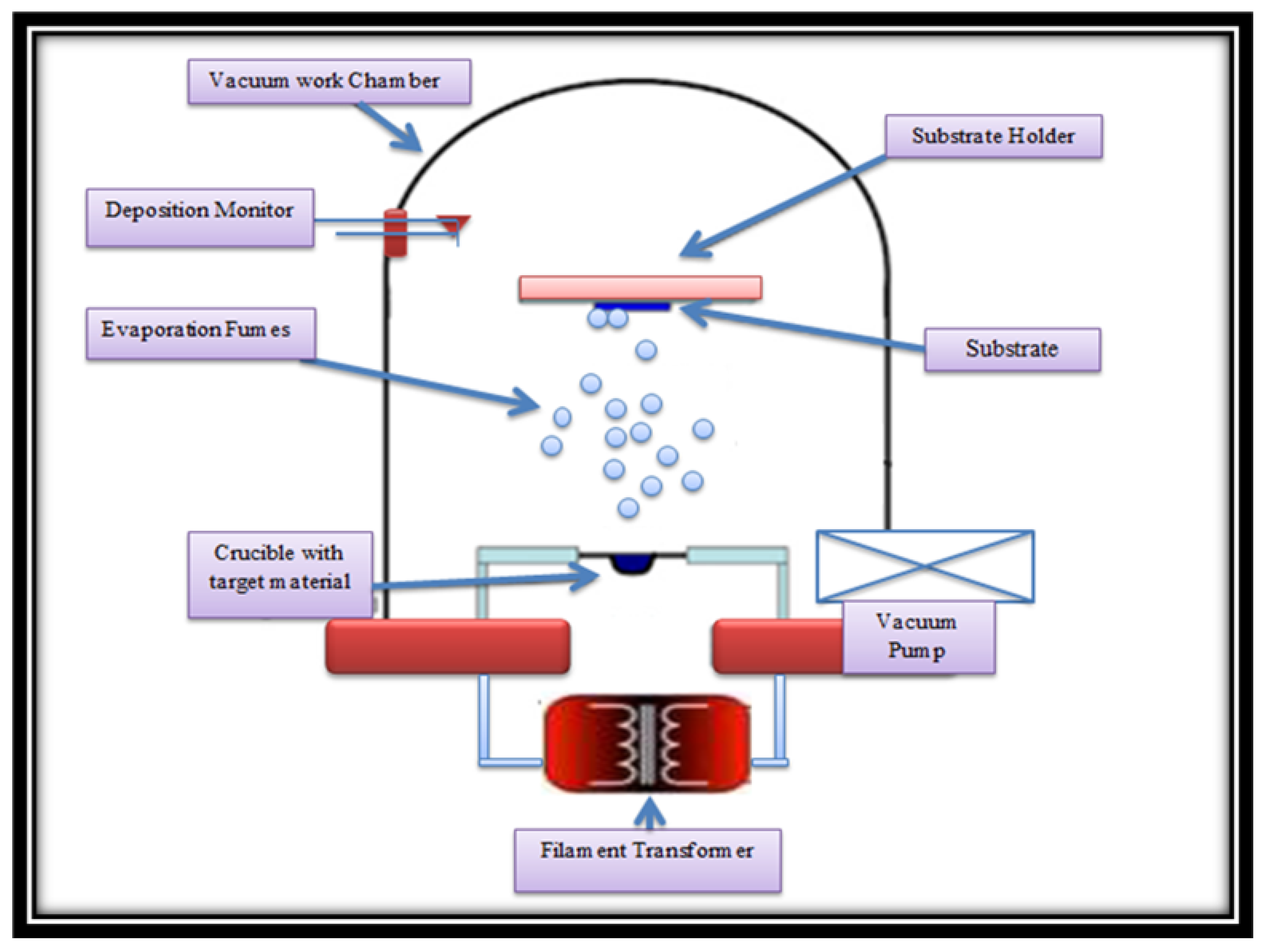
Figure 1. Schematic representation of S n O 2 / C u O thin-film deposition via physical vapor deposition.
Nanomaterials 15 01748 g001
Figure 2. Schematic representation of S n O 2 / C u O thin-film annealing via chemical vapor deposition.
Nanomaterials 15 01748 g002
Figure 3. XRD patterns of (a) as-deposited S n O 2 , (b) S n O 2 /CuO-400 °C, (c) S n O 2 /CuO-500 °C, and (d) S n O 2 /CuO-600 °C thin films.
Nanomaterials 15 01748 g003
Figure 4. SEM images of (a) as-deposited S n O 2 , (b) S n O 2 / C u O -400 °C, (c) S n O 2 / C u O -500 °C, and (d) S n O 2 / C u O -600 °C.
Nanomaterials 15 01748 g004
Figure 5. Transmittance spectra of (a) as-deposited S n O 2 , (b) S n O 2 /CuO-600 °C, (c) as deposited CuO (d) S n O 2 /CuO-500 °C, and (e) S n O 2 /CuO-400 °C.
Nanomaterials 15 01748 g005
Figure 6. Tauc plot for as-deposited S n O 2 (a) as-deposited C u O (b) S n O 2 / C u O -400 °C (c) S n O 2 / C u O -500 °C (d) S n O 2 / C u O °C (e).
Nanomaterials 15 01748 g006
Figure 7. Plausible reaction mechanism of S n O 2 / C u O heterostructure thin-film-based photocatalyst for H2 generation under solar light irradiation.
Nanomaterials 15 01748 g007
Figure 8. LSV graphs of pure S n O 2 (a), pure C u O (b), S n O 2 / C u O -400 °C (c), S n O 2 / C u O -500 °C (d), S n O 2 / C u O -600 °C, (e) thin films under dark and light conditions.
Nanomaterials 15 01748 g008
Figure 9. Solar-to-hydrogen conversion graph.
Nanomaterials 15 01748 g009
Table 1. Solar light-to-hydrogen conversion efficiencies of S n O 2 , C u O , S n O 2 / C u O -400 °C, S n O 2 / C u O -500 °C, S n O 2 / C u O -600 °C.
Samples NameSTH%Reference
T i O 2 (anatase)0.02 Arora et al. (2023) [37]
W O 3 0.05 Arora et al. (2023) [37]
C u 2 O 0.10–0.15 Xiao et al. (2023) [38]
S n O 2 3.70 × 10 5 This work
C u O 1.60 × 10 4 This work
S n O 2 / C u O at 400 °C 1.56 × 10 1 This work
S n O 2 / C u O at 500 °C 1.33 × 10 1 This work
S n O 2 / C u O at 600 °C 2.5 × 10 1 This work
Disclaimer/Publisher’s Note: The statements, opinions and data contained in all publications are solely those of the individual author(s) and contributor(s) and not of MDPI and/or the editor(s). MDPI and/or the editor(s) disclaim responsibility for any injury to people or property resulting from any ideas, methods, instructions or products referred to in the content.