Article

Interface-Driven Electrothermal Degradation in GaN-on-Diamond High Electron Mobility Transistors

Institute of Micro/Nano Electromechanical System and Integrated Circuit, College of Mechanical Engineering, State Key Laboratory for Modification of Chemical Fibers and Polymer Materials, Donghua University, Shanghai 200051, China
*
Authors to whom correspondence should be addressed.
Nanomaterials 2025, 15(14), 1114; https://doi.org/10.3390/nano15141114
Submission received: 9 June 2025 / Revised: 3 July 2025 / Accepted: 14 July 2025 / Published: 18 July 2025

Abstract

Diamond is an attractive substrate candidate for GaN high-electron-mobility transistors (HEMT) to enhance heat dissipation due to its exceptional thermal conductivity. However, the thermal boundary resistance (TBR) at the GaN–diamond interface poses a significant bottleneck to heat transport, exacerbating self-heating and limiting device performance. In this work, TCAD simulations were employed to systematically investigate the effects of thermal boundary layer (TBL) thickness (dTBL) and thermal conductivity (κTBL) on the electrothermal behavior of GaN-on-diamond HEMTs. Results show that increasing the TBL thickness (5–20 nm) or decreasing its thermal conductivity (0.1–1.0 W/(m·K)) leads to elevated hotspot temperatures and degraded electron mobility, resulting in a notable deterioration of IV characteristics. The nonlinear dependence of device performance on κTBL is attributed to Fourier’s law, where heat flux is inversely proportional to thermal resistance. Furthermore, the co-analysis of substrate thermal conductivity and interfacial quality reveals that interface TBR has a more dominant impact on device behavior than substrate conductivity. Remarkably, devices with low thermal conductivity substrates and optimized interfaces can outperform those with high-conductivity substrates but poor interfacial conditions. These findings underscore the critical importance of interface engineering in thermal management of GaN–diamond HEMTs and provide a theoretical foundation for future work on phonon transport and defect-controlled thermal interfaces.

Graphical Abstract

1. Introduction

Gallium nitride (GaN) has emerged as a leading material for fabricating high-performance transistors due to its wide bandgap, high saturation electron drift velocity, and superior breakdown characteristics [1,2]. Among GaN-based devices, the high-electron-mobility transistor (HEMT) is particularly attractive for high-power and high-frequency applications. However, under such operating conditions, a localized thermal imbalance leads to an extremely high temperature at the hotspot, typically located between the drain and gate of the HEMT, causing a reduction in the drain current [3]. This phenomenon, known as the self-heating effect [4], imposes significant challenges on both the performance and reliability GaN HEMTs. Self-heating is critically linked to the Arrhenius dependence of the mean time to failure (MTTF) on temperature. Empirical data shows a 50% reduction in MTTF per 10–15 K increase under normal operating conditions [5,6]. Notably, for GaN HEMTs designed to operate at 400–500 K, seemingly marginal temperature increases of 10 K (representing just 2–2.5% of the operating temperature) can precipitate disproportionate degradation effects [7,8,9]. Therefore, maintaining the hotspot temperature within a safe operating range, while maximizing output power density, has become a central focus in GaN device research [10]. Over the past few decades, several methods and techniques are proposed for device thermal management, including heat pipes, air cooling, phase change material cooling, thermoelectric cooling, etc. Among these, replacing the substrate with a material of higher thermal conductivity stands out as one of the most direct and effective approaches [11]. Conventional substrates for GaN, such as sapphire, SiC, and Si, offer thermal conductivities ranging from 40 to 400 W/(m·K), which limit the thermal performance of GaN devices. In contrast, diamond with a thermal conductivity exceeding 1800 W/(m·K) offers a compelling alternative, substantially enhancing the device’s thermal management [12], especially since currently, industrial-scale diamond can be synthesized at a reasonable cost [13].
However, despite diamond’s intrinsic thermal advantages, the overall heat dissipation efficiency of GaN-on-diamond structures is significantly influenced by the thermal boundary resistance (TBR) at the GaN–diamond interface. TBR is primarily attributed to several factors, including an acoustic mismatch between GaN and diamond, the dielectric interlayer used for diamond growth seeding, the low-density damaged layer that forms on the diamond surface, and the defective transition region near the diamond nucleation surface [14,15]. To address this challenge, several interface engineering approaches have been explored. Zhou attempted to directly grow diamond on GaN without spacers, aiming to achieve an ideal interface (TBR = 3 m2·K/GW) [16,17]. However, interface degradation during diamond growth led to a significantly higher TBR of 61.1 m2·K/GW, and the resulting diamond layer exhibited a thermal conductivity of only 180 W/(m·K). In contrast, Zhou and Field introduced thin dielectric interlayers, such as 5 nm SiN, 5 nm AlN, and 10 nm SiC, as nucleation spacers. These configurations yielded TBR values of 6.5 m2·K/GW, 38.5 m2·K/GW, and 35 m2·K/GW respectively, while achieving diamond thermal conductivities of 500 W/(m·K), 900 W/(m·K), and 1500 W/(m·K) [18,19]. Additionally, Mu et al. employed the surface activated bonding (SAB) technique, which enables bonding GaN to bulk diamond at room temperature using a thin adhesion layer [20]. This method achieved a minimum TBR of 11 m2·K/GW, although it involved a complex fabrication process [21].
Based on these experimental insights, three critical parameters have been identified for accurate thermal modeling: interlayer thickness parameters, interlayer thermal conductivity, and substrate diamond thermal conductivity. To investigate the influence of GaN–diamond TBR on device characteristics, we conducted a comprehensive simulation study using Silvaco technology computer-aided design (TCAD) tools. By systematically varying the thermal and structural properties of the interface, we analyzed their effects on key performance metrics, including the peak drain current, hotspot temperature, and electron mobility. Our findings provide a mechanistic understanding of TBR-governed self-heating in GaN HEMTs, offering design guidelines for improved thermal management. This work lays a theoretical framework for future studies of ballistic transport and interface-level energy dissipation phenomena in GaN-on-diamond systems.

2. Device Details and Simulation Methods
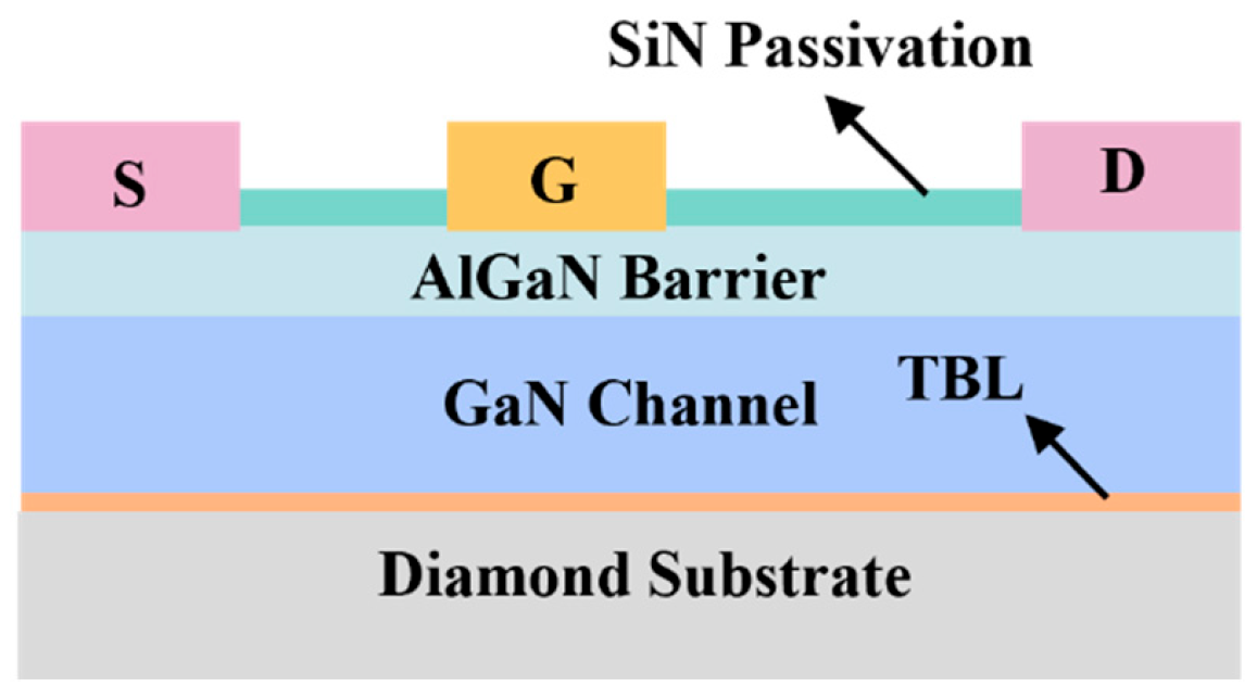
2.1. Device Model

The simulated GaN HEMT structure is illustrated in Figure 1. It consists of a SiN passivation layer, an Al0.25Ga0.75N barrier layer, a GaN buffer layer, a thermal boundary layer (TBL), and an underlying substrate, wherein Al0.25Ga0.75N was chosen as the barrier layer to achieve an optimal balance between electronic performance and structural stability. According to Zhang et al., while increasing Al content enhances the 2DEG density via a larger conduction band offset, excessive Al (x > 0.3) leads to reduced mobility due to alloy scattering and interface roughness [22]. Miyoshi et al. further reported that a high Al composition induces significant strain and misfit dislocations, degrading the crystal quality [23]. Moreover, Hang et al. showed that ~65% of the bandgap difference in AlxGa1-xN/GaN heterostructures contributes to conduction band offset; for x = 0.25, this yields ~0.3 eV, sufficient for effective electron confinement [24]. Therefore, x = 0.25 offers a well-balanced trade-off among the 2DEG density, carrier mobility, and structural integrity. Among various GaN-on-diamond fabrication techniques, this study adopts direct epitaxial growth as the reference methodology, since it provides a more controllable and idealized interface, which is critical for evaluating thermal boundary resistance effects with minimal structural variability.
The detailed device parameters are listed in Table 1. The lateral dimension of the simulated GaN device is 10.4 µm, and the electrode thickness is set to 0.2 µm. The gate metal has a work function of 4.2 eV, forming a Schottky contact with the Al0.25Ga0.75N layer. It is important to note that the Schottky contact does not inject electrons but instead serves as an extraction point for high-energy electrons that acquire sufficient kinetic energy to surmount the potential barrier and reach the electrode [25]. This simple structure is an ideal choice for analyzing the underlying physics of electron transport and self-heating effects in GaN HEMT. Its moderate complexity enables a detailed investigation of the interplay between thermal and electronic behavior, while maintaining computational feasibility for TCAD simulations.

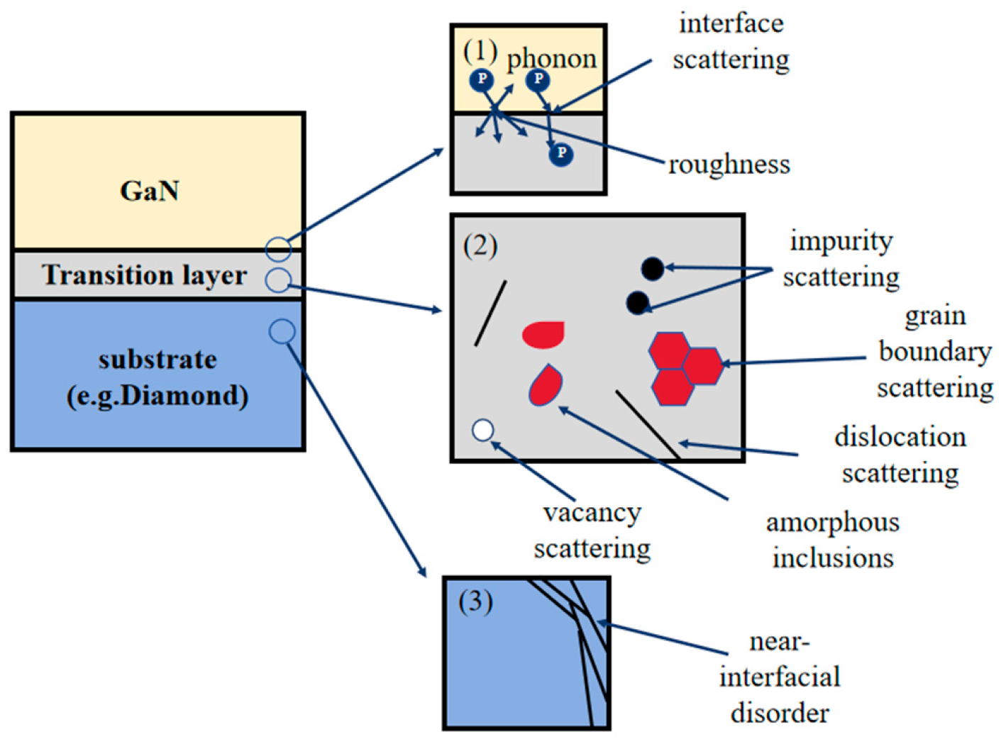
2.2. Simulation Methodologies

In this work, the electronic and thermal characteristics of the GaN HEMT were simulated using the Silvaco TCAD platform. This simulation environment incorporates a suite of advanced physical models that closely replicate real device behavior, enabling a comprehensive analysis of both electrical and thermal performance [1]. The core of the simulation is based on solving the coupled Poisson equation and the carrier continuity equations under the drift-diffusion model, augmented by models for carrier statistics, collision ionization, carrier lifetime, mobility, and the generation–recombination process accurately.
Prior research have shown that variations in the microstructure and properties of the TBL significantly influence the electrical characteristics of GaN-based devices [26]. However, the underlying mechanisms by which TBL parameters impact device performance remain inadequately understood. In this work, we adopt a bottom-up approach, that starts with macroscopic current–voltage characteristics, then progressively decouples and analyzes the influences of individual microscopic parameters to elucidate these fundamental mechanisms. The electronic transport in the simulation is modeled using the drift-diffusion formalism derived from the Boltzmann transport equation. It is important to note that this derivation assumes the validity of the Einstein relation, which links the carrier mobility and diffusion coefficient [27]. The electron current density is obtained by:
J n = q D n n q n μ n Ψ μ n n k B T L l n n i e
where q is the elementary charge, Dn is the electron diffusivity dependent on temperature and mobility, n is the electron concentration, μn is electron mobility, kB is the Boltzmann constant, nie is the effective intrinsic carrier concentration, and TL is the lattice temperature.
Given that excessive heat generation is a primary reliability concern in GaN HEMTs, especially in the hotspot region between the gate and drain [28], the accurate modeling of temperature distribution is essential. To address this problem, we incorporate the lattice heating model, which introduces the heat flow equation into the computational framework. Its general form is expressed as:
T L t = κ T L + H
where C is the heat capacity per unit volume, κ is the thermal conductivity, H is the heat generation rate, and TL is the lattice temperature. The thermal conductivities employed in our simulations at room temperature (300 K) are summarized in Table 2.
Thermal conductivity in semiconductors is known to be temperature-dependent and follows a power law of the form [32]:
κ L T = κ L 300 K T 300 α
κ L (300 K) is the thermal conductivity of materials at 300 K. α is a quantitative parameter characterizing the temperature dependence of thermal conductivity (e.g., α = −0.28 for GaN) [33].
The accuracy of temperature distribution simulations is critical for modeling the localized hotspot and overall heat transfer process. Therefore, the heat exchange between the device and the external environment should also be considered carefully. Prior studies indicate that the impact of lateral heat dissipation through the device sidewalls is negligible [6,34]. Therefore, in our simulation, heat is assumed to be extracted only through the bottom Dirichlet boundary, while all other boundaries are set as adiabatic [35].
Equation (1) demonstrates the influence of electron mobility on current density, highlighting the necessity of accurate mobility models. Furthermore, considering the well-documented temperature dependence of electron mobility [36], we employed temperature-dependent high-field/low-field mobility models (GANSAT and ALBRCT), ensuring high simulation fidelity [11,34].
The core objective of this work is to investigate how TBR at the GaN–diamond interface affects electrical performance, particularly current characteristics. Consequently, accurate modeling of TBR becomes critically important. Figure 2 illustrates the principal mechanisms responsible for TBR formation at GaN–diamond interface, including: (1) phonon scattering at the GaN–diamond interface; (2) scattering from defects, dislocations, and other imperfections within the transition layer; and (3) disorder-induced scattering near the interface region [16]. These three mechanisms hinder phonon transmission across the interface, leading to increased TBR. Since phonons are the dominant heat carriers in semiconductors (with negligible contribution from electrons), only phonon-mediated heat transport is considered in this study [37].
To simulate TBR, TBL is introduced at the GaN–diamond interface [38]. The TBR is modeled using the relationship:
T B R = d T B L κ T B L
where dTBL is thickness of the thermal boundary layer and κTBL is the thermal conductivity of the TBL. This approach enables us to precisely investigate the impact of interfacial heat transfer resistance on the thermal and electrical behavior of GaN-on-diamond HEMTs. While atomistic features such as vacancies, amorphous transition regions, and grain boundaries are not explicitly resolved in the Silvaco TCAD framework, their impact is embedded in these parameters based on well-established physical insights. Prior studies have shown that amorphous layers, voids, misorientation defects, and vacancy scattering all contribute to increased thermal boundary resistance and spatially extended interfacial scattering [18,39,40]. Experimental measurements have further confirmed that interfacial thermal conductance correlates strongly with bonding quality and morphology [21]. Building upon our previous modeling framework, which introduced κTBL and dTBL as physically grounded descriptors of interfacial degradation, we extend this approach here to study the device-level consequences of realistic GaN–diamond interfaces [41].

3. Simulation Results and Discussion

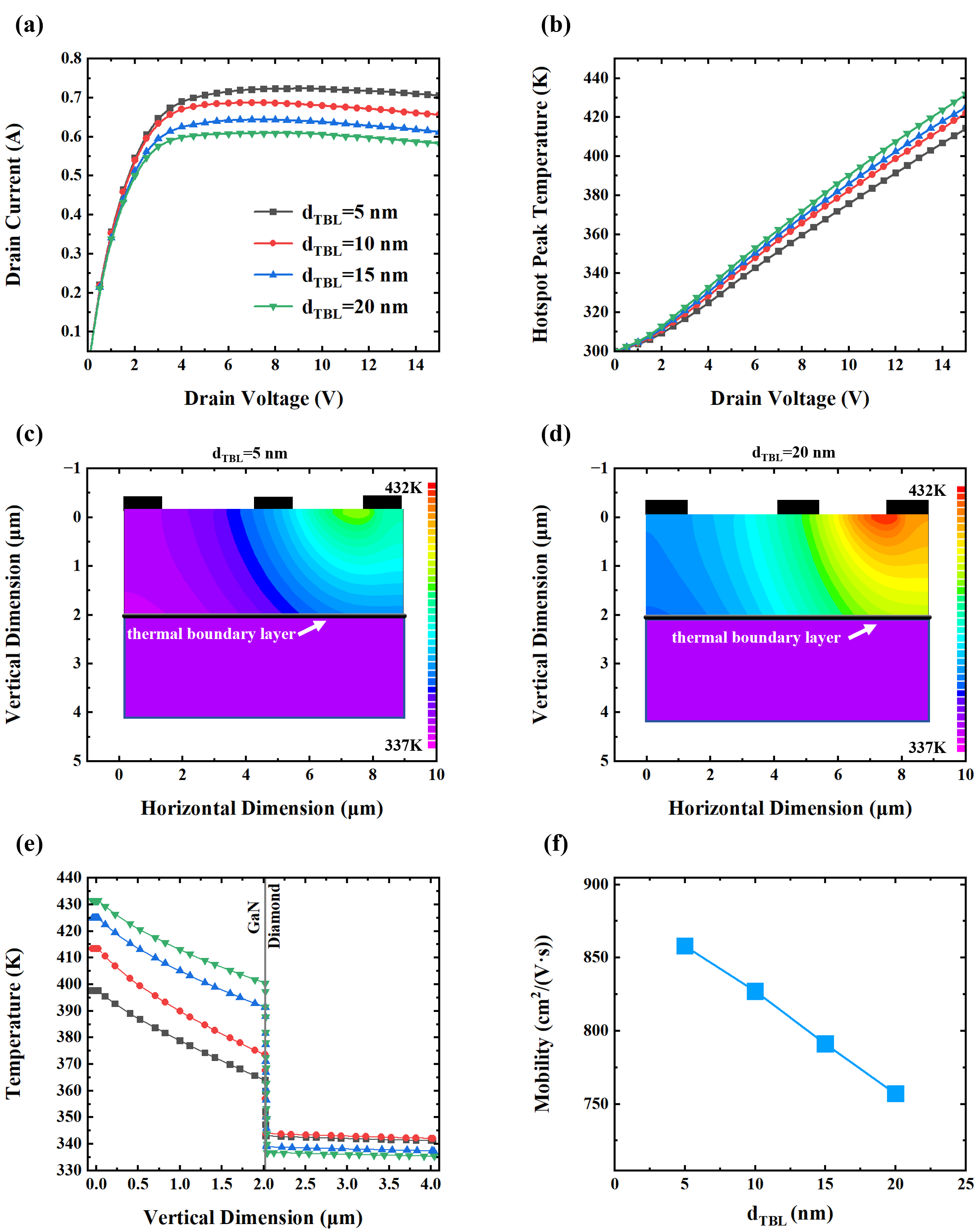
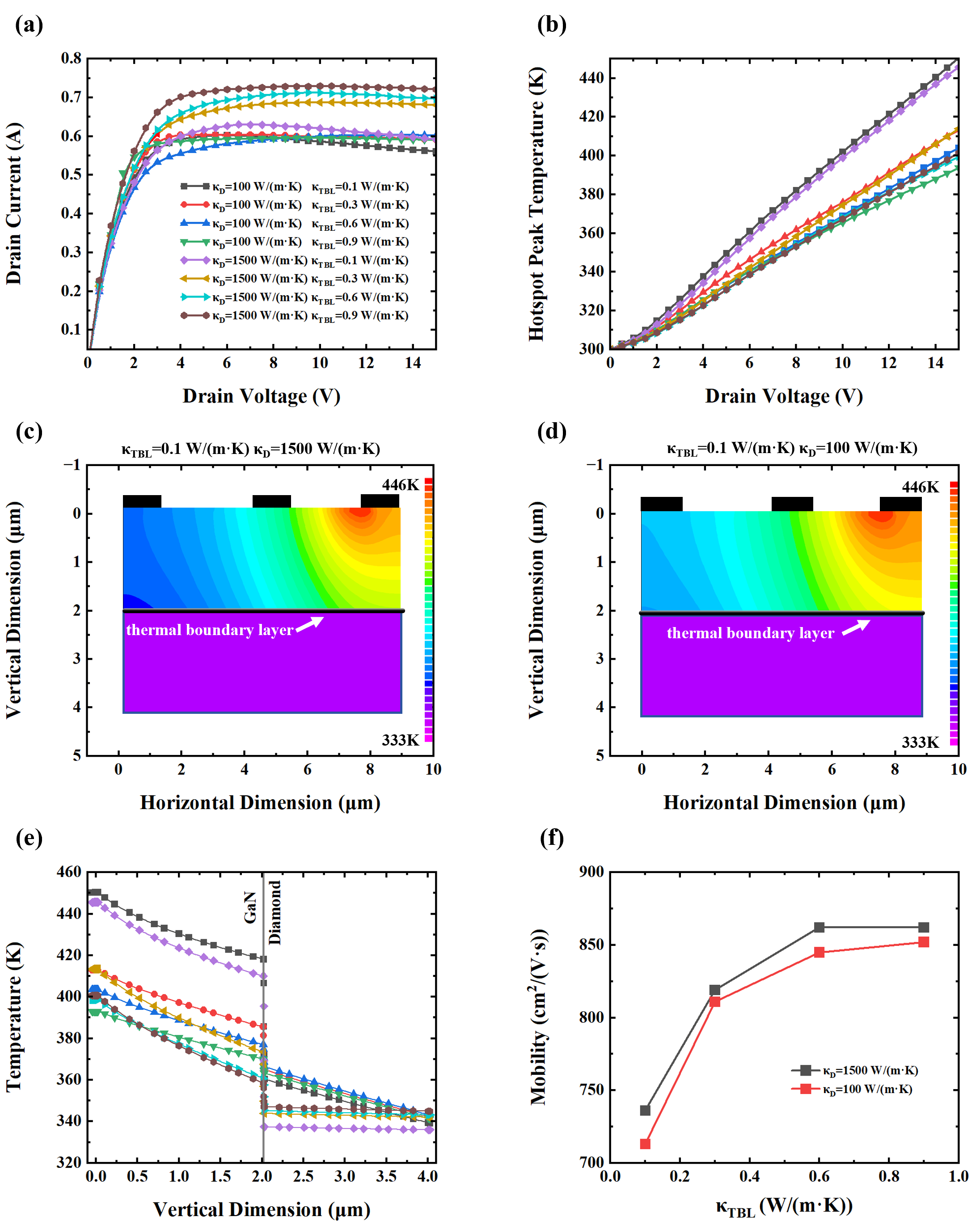
3.1. Effect of Thermal Boundary Layer Thickness

Experimental studies have revealed that during the direct growth of GaN-on-diamond, ion flux excitation can induce atomic interdiffusion and interfacial amorphization, which significantly affect interfacial heat transport [20,21]. Based on experimentally observed diffusion thicknesses in the range of 5–20 nm and measured TBR values between 12.5 and 50 m2·K/GW, the thermal conductivity of the TBL in the simulations is set to κTBL = 0.4 W/(m·K), in accordance with Equation (4).
As shown in Figure 3a, increasing the dTBL results in a clear degradation in electrical performance. The peak drain current, especially, decreases from 0.723 A to 0.608 A as dTBL increases from 5 nm to 20 nm, corresponding to relative reductions of 4.98%, 5.95%, and 4.98% across incremental thicknesses, respectively. This trend is consistent with the literature, which identifies excessive self-heating, particularly in hotspot regions, as a primary degradation mechanism in GaN HEMTs [28]. The relationship between the peak hotspot temperature and the drain voltage is shown in Figure 3b. The hotspot temperature of the device increases linearly with the increase in drain voltage, and the peak temperature rises from 414 K to 431 K with the increasing dTBL. Figure 3c and Figure 3d illustrate the spatial temperature distribution for TBL thicknesses of 5 nm and 20 nm, respectively. A thicker TBL results in a significantly higher localized temperature, particularly around the hotspot region.
Figure 3e presents the vertical temperature distribution within the device (horizontally located at 7 µm), traversing the channel. The central hotspot exhibits a relatively flat and elevated temperature plateau, indicative of substantial heat accumulation. Simultaneously, the lattice temperature decreases with the increase in distance from the hotspot, and the decreasing trend of lattice temperature tends to be flat with the increase in distance, indicating enhanced thermal conduction in the GaN with the decrease in temperature. Notably, when the dTBL increases from 5 nm to 20 nm, the interfacial temperature difference rises from 22.3 K to 63.6 K. This confirms that an increased dTBL inhibits thermal transport across GaN–diamond interface, exacerbating local heating.
As described by Equation (1), electron mobility is a critical factor directly governing current density. Figure 3f demonstrates that the peak electron mobility in the channel layer decreases linearly from 858 cm2/(V·s) to 757 cm2/(V·s) with an increasing dTBL. This trend aligns well with the temperature-dependent Hall effect measurements, which demonstrate that elevated temperatures enhance phonon activity and consequently increase phonon scattering rates and reduce carrier mobility [42,43].
The simulation results offer insight into the underlying mechanisms through which the dTBL affects device characteristics. As the dTBL increases, phonons experience extended transport paths and are more likely to scatter with interfacial defects, impurities, or amorphous structures. Moreover, an increased TBL thickness is typically associated with a higher degree of interfacial disorder, further impeding phonon transmission. Although the current work does not explicitly simulate atomic-scale defects or calculate phonon mean free paths, this behavior is strongly supported by our previous simulation studies. In the study of Wang et al., we demonstrated that amorphous interlayers at GaN/AlN interfaces induce significant phonon mode conversion, inelastic scattering, and phonon localization, all of which become more prominent with an increased interlayer thickness [44,45]. Similarly, in the study of Liu et al., compositionally diffused interfaces were shown to reduce interfacial thermal conductance as a function of diffusion thickness due to enhanced phonon scattering across the graded region [46]. These findings indicate that even without explicitly modeling point defects, the increase in dTBL can be physically linked to degraded phonon transport through morphological and compositional disorder.
These phenomena are captured in the simulations through an equivalent TBR, which effectively suppresses interfacial heat transfer. The resulting heat accumulation elevates the temperature of the GaN channel, which in turn reduces the material’s thermal conductivity, creating a positive feedback loop that further impedes heat dissipation and exacerbates hotspot formation.
Ultimately, elevated temperatures in the two-dimensional electron gas (2DEG) channel reduce electron mobility, resulting in the deterioration of the device’s electrical performance. These findings highlight the critical role of interfacial thermal engineering in the design and optimization of GaN-on-diamond HEMTs.

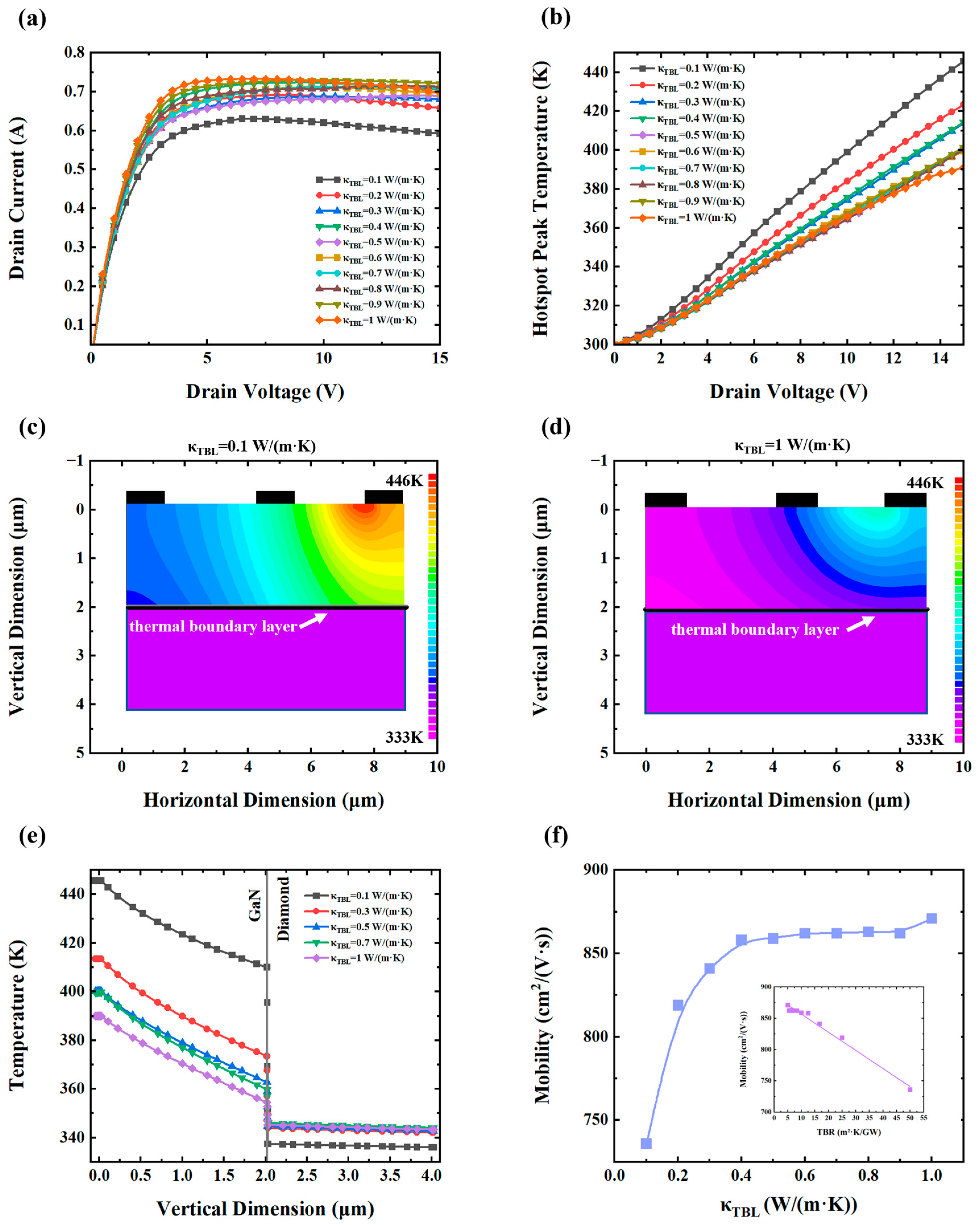
3.2. Effect of Thermal Boundary Layer Thermal Conductivity

During the GaN-on-diamond fabrication process, ion beam-induced damage near the interface introduces a high defect density, including dislocations and vacancies. These defects substantially reduce local thermal conductivity compared to the bulk material, with the extent of degradation strongly dependent on processing parameters. To investigate the influence of κTBL on device performance, a systematic parameter sweep was conducted across a TBR range of 5–50 m2·K/GW, derived from simulation data. A dTBL was fixed at 5 nm in the simulations to effectively isolate the effects of the κTBL from those of the layer thickness, thereby enabling a focused analysis of the κTBL’s impact on the device’s electrical performance.
As shown in Figure 4a, the κTBL significantly affects the peak drain current. When the κTBL is 1 W/(m·K), the peak current reaches 0.733 A. However, when the κTBL decreases to 0.1 W/(m·K), the peak current drops to 0.629 A, a reduction of approximately 14.1%. This decline is attributed to intensified self-heating, which limits carrier mobility and current conduction. As shown in Figure 4b, the hotspot peak temperature increases significantly as the κTBL decreases. Specifically, for κTBL = 1 W/(m·K), the hotspot peak temperature reaches 391.1 K, while for κTBL = 0.1 W/(m·K), it rises to 445.7 K. Notably, a nonlinear trend is observed: reducing the κTBL from 1 W/(m·K) to 0.5 W/(m·K) increases the hotspot peak temperature by only 9.1 K (2.3%), whereas a further reduction to 0.1 W/(m·K) results in a sharp 45.5K rise (11.6%). This suggests a threshold behavior where thermal transport begins to degrade rapidly below a certain κTBL.
Figure 4c and Figure 4d depict the spatial temperature distributions for κTBL = 0.1 and 1 W/(m·K), respectively. The lower κTBL case shows significantly higher overall temperatures, especially in hotspot regions, indicating inefficient heat dissipation.
Figure 4e presents the vertical temperature profile of the device, revealing that the interfacial temperature jump also exhibits pronounced nonlinearity. For κTBL = 1 W/(m·K), the temperature jump at the interface is 9.3 K, which increases to 72.6K when the κTBL drops to 0.1 W/(m·K). Notably, the decrease from 1 W/(m·K) to 0.5 W/(m·K) causes only an 8.3 K rise (89.2%), whereas the decrease from 0.5 W/(m·K) to 0.1 W/(m·K) results in a dramatic 55 K rise (591.3%). These findings further emphasize the critical importance of maintaining adequate interfacial thermal conductivity for effective heat dissipation.
Figure 4f shows the relationship between the κTBL and electron mobility in the 2DEG channel. Electron mobility exhibits a sharp decline when the κTBL is below 0.4 W/(m·K), highlighting a threshold behavior. This abrupt change suggests that reduced thermal transport at the interface significantly impacts phonon dynamics, increasing phonon scattering and thereby limiting carrier mobility. When plotted as TBR versus mobility (inset), a linear relationship emerges, consistent with expectations from the heat transfer theory. According to Fourier’s law, thermal resistances in the series are analogous to the series model of electrical resistances, whereas the use of thermal conductance requires reciprocal processing.
In the simulations, a TBL is placed between two thermal conductors. The heat flux across the interface is calculated as:
H = T T B R
Since TBR is defined as Equation (4), the inverse relationship between the κTBL and TBR leads to the observed nonlinear dependence of mobility on the κTBL, despite the linearity between mobility and TBR.
Based on the aforementioned analysis, reductions in the κTBL stem primarily from bombardment-induced defect accumulation at the interface, which enhances phonon scattering. The phonon mean free path is shortened during thermal transport and thus, raises the effective TBR. While no explicit defect-scattering model is implemented, the degradation of electron mobility in this study is modeled using field- and temperature-dependent mobility parameters derived from established scattering-based transport models. Specifically, the models are based on the Monte Carlo simulation framework developed by Farahmand et al., which accounts for key scattering mechanisms including polar and non-polar optical phonons, acoustic phonons, ionized impurities, alloy disorder, and piezoelectric interactions [47]. Although individual defects are not explicitly modeled, the cumulative effect of phonon-related scattering caused by interfacial disorder is implicitly captured through the reduced mobility values in the simulation. This interpretation is further supported by recent studies on electrically driven phonon transport manipulation in two-dimensional heterostructures, where enhanced phonon scattering—induced by interface disorder or external perturbation—has been shown to significantly degrade carrier mobility via strengthened phonon–electron coupling [48]. These effects impede heat exchange between GaN and diamond, resulting in elevated hotspot temperatures and degraded carrier transport, mirroring the performance deterioration previously described for an increased TBL thickness.

3.3. Effect Substrate and Thermal Boundary Layer Thermal Conductivity

Experimental observations have shown that even under identical interface conditions, the thermal conductivity of diamond substrates grown by different methods can vary significantly. Particularly when employing direct diamond growth on GaN, the substantial 13% lattice mismatch (GaN: a = 3.189 Å and diamond: a = 3.567 Å) induces pronounced crystalline defects and TBR variability [30,49,50]. As demonstrated by Zhou et al., diamond films grown under identical process conditions exhibit thermal conductivity variations of 200–1000 W/m·K as increased thickness promotes larger grain coalescence [16,25,51]. To evaluate the combined influence of the diamond substrate and TBL on device behavior, simulations were conducted under identical interfacial conditions using both high (1500 W/(m·K)) and low (100 W/(m·K)) thermal conductivity diamond substrates. This approach enabled a comparative analysis of device characteristics under varying substrate qualities and interfacial scenarios.
The IV characteristics of devices with high thermal conductivity and low thermal conductivity diamond substrates under varying κTBL values are shown in Figure 5a. When the κTBL decreased from 0.9 W/(m·K) to 0.1 W/(m·K), the peak drain current of HEMT devices with high thermal conductivity diamond substrates dropped by 0.099 A (13.6%) due to pronounced self-heating effects, while the corresponding current reduction with low thermal conductivity substrates (100 W/(m·K)) was only 0.02 A (3.34%). This significant difference indicates that devices with high thermal conductivity diamond substrates are more sensitive to changes in interfacial thermal resistance. Even minor increases in interfacial thermal resistance can result in substantial performance degradation, whereas devices with inherently poor heat dissipation (low κd) display a relatively muted response to such variations.
Figure 5b reveals that the peak hotspot temperature increased by 44.3 K (11%) in high κd devices and by 53.7 K (13.6%) in low κd devices when the κTBL changed from 0.9 W/(m·K) to 0.1 W/(m·K). Interestingly, as shown in Figure 5c,d, both device types exhibit similar temperature distributions when κTBL = 0.1 W/(m·K), despite their vastly different substantial substrate thermal conductivity. This suggests that, under severe interfacial thermal resistance conditions, the substrate’s intrinsic thermal conductivity becomes secondary to the bottleneck imposed by the TBL. Figure 5e further supports this observation by illustrating nearly identical vertical temperature profiles in both devices, confirming that interfacial thermal resistance dominates overall heat transport. These findings imply that the TBL imposes a comparable suppression of heat flow in both high- and low-conductivity substrates. However, the operational consequences differ: in high-κd devices, the degradation is more dramatic because they are transitioning from an initially high-performance state. Conversely, devices with low κd substrates operate from the outset in a limited thermal regime and thus experience smaller performance deltas in response to interfacial degradation. These findings are consistent with previous studies on the effects of substrate materials in device reliability and efficiency [34,52]. Figure 5f shows that electron mobility decreases with increasing TBR for both substrate types, consistent with earlier analyses of κTBL-dependent mobility. Notably, in devices with high κd substrates, a sufficiently poor κTBL causes the electron mobility to degrade to the level of low κd devices that possess superior interfacial thermal properties. This degradation is also reflected in the current output: under severely degraded interface conditions, devices with excellent bulk thermal substrates may underperform relative to those built on poorer substrates with better interface quality.
These findings underscore the critical importance of optimizing not only the substrate material but also the quality of the GaN–diamond interface. Even with a high-κd diamond, poor interfacial thermal transport can negate the substrate’s advantages and significantly impair device performance.

4. Summary and Conclusions

This study systematically investigated the thermal management challenges in diamond-based GaN HEMTs through comprehensive TCAD simulations, with particular focus on the interfacial TBR at the GaN–diamond interface. Although diamond substrates with high intrinsic thermal conductivity offer exceptional heat dissipation potential, their effectiveness is often compromised by interfacial imperfections, which introduce substantial TBR and severely limit heat flow, thereby exacerbating the device self-heating effect. By varying the thickness of the TBL, it was demonstrated that an increased interface thickness significantly elevated the hotspot temperature and reduced electron mobility, resulting in degraded output characteristics. Similarly, adjusting the TBL thermal conductivity κTBL revealed that lower conductivity layers induced a steep rise in hotspot temperature and a notable decline in electron mobility. This degradation in device performance arises from the nonlinear dependence between the κTBL and electron mobility, governed by Fourier’s law and the inverse relationship between heat flux density and thermal resistance. Furthermore, a comparative analysis between high and low thermal conductivity diamond substrates under identical interfacial conditions highlighted that high-κd substrates were substantially more sensitive to TBR variations. Under severe interface degradation, devices with high-κd diamond showed a 13.6% reduction in peak current, whereas those with low-κd diamond exhibited only a 3.34% reduction. Crucially, the simulations revealed a counterintuitive result: devices with optimized interfaces on low-κd substrates could outperform those with high-κd substrates suffering from poor interfacial quality. This finding underscores the dominant role of interface engineering over substrate thermal conductivity in achieving optimal device performance.
The insights from this work provide valuable reference data, including temperature field distributions, electron mobility profiles, and interfacial transport parameters, that can be directly utilized in the microscale modeling of GaN–diamond systems. Moreover, these results establish a theoretical foundation for future studies on ballistic phonon transport, interfacial defect dynamics, and advanced thermal management strategies. This study investigated the electrical behavior of diamond-based GaN structures under ambient temperature conditions (>300 K). The findings provide a foundational framework for extending our exploration into the cryogenic domain (4–300 K), enabling an in-depth investigation of low-temperature phenomena such as diamond’s maximized thermal conductivity and suppressed phonon scattering. Overall, this work advances the understanding of thermal transport bottlenecks in GaN-on-diamond devices and offers practical guidance for interface optimization in next-generation high-power electronics.

Author Contributions

Methodology, Y.L., A.U. and C.Z.; Validation, Y.L. and X.L.; Formal analysis, J.S., Y.X. and G.C.; Investigation, H.W., A.U., Y.X., P.G. and G.C.; Resources, P.G.; Data curation, X.D., J.S. and X.L.; Writing—original draft, H.W.; Writing—review & editing, G.C. and X.L.; Visualization, X.D.; Supervision, X.L. All authors have read and agreed to the published version of the manuscript.

Funding

This research was funded by the National Natural Science Foundation of China (Grant Nos. 12374027, 52206080, 12304039, and 52306102), the National Key Research and Development Program of China (Grant No. 2023YFB3210900), the Shanghai Committee of Science and Technology (Grant No. 21TS1401500), and the 2025 Donghua University Discipline Development and Research Capability Enhancement Project.

Data Availability Statement

The original contributions presented in this study are included in the article. Further inquiries can be directed to the corresponding author.

Conflicts of Interest

The authors declare no conflict of interest.

References

  1. Chang, C.-Y.; Douglas, E.; Kim, J.; Lu, L.; Lo, C.-F.; Chu, B.-H.; Cheney, D.; Gila, B.P.; Ren, F.; Via, G.D.; et al. Electric-field-driven degradation in off-state step-stressed AlGaN/GaN high-electron mobility transistors. IEEE Trans. Device Mater. Reliab. 2011, 11, 187–193. [Google Scholar]
  2. Nigam, A.; Bhat, T.N.; Rajamani, S.; Dolmanan, S.B.; Tripathy, S.; Kumar, M. Effect of self-heating on electrical characteristics of AlGaN/GaN HEMT on Si (111) substrate. AIP Adv. 2017, 7, 085015. [Google Scholar] [CrossRef]
  3. Hu, B.; Wang, Z.; Xu, K.; Tang, D. Hotspot and nonequilibrium thermal transport in AlGaN/GaN FinFET: A coupled electron-phonon Monte Carlo simulation study. Int. J. Heat Mass Transf. 2025, 241, 126679. [Google Scholar] [CrossRef]
  4. Chang, Y.; Zhang, Y.; Zhang, Y.; Tong, K. A thermal model for static current characteristics of AlGaN/GaN high electron mobility transistors including self-heating effect. J. Appl. Phys. 2006, 99, 044501. [Google Scholar]
  5. Lee, S.; Vetury, R.; Brown, J.D.; Gibb, S.R.; Cai, W.Z.; Sun, J.; Green, D.S.; Shealy, J. Reliability assessment of AlGaN/GaN HEMT technology on SiC for 48V applications. In Proceedings of the 2008 IEEE International Reliability Physics Symposium, Phoenix, AZ, USA, 27 April–1 May 2008; pp. 446–449. [Google Scholar]
  6. Wang, A.; Tadjer, M.; Calle, F. Simulation of thermal management in AlGaN/GaN HEMTs with integrated diamond heat spreaders. Semicond. Sci. Technol. 2013, 28, 055010. [Google Scholar]
  7. Jeon, D.-Y.; Koh, Y.; Cho, C.-Y.; Park, K.-H. Impact of temperature-dependent series resistance on the operation of AlGaN/GaN high electron mobility transistors. AIP Adv. 2021, 11, 115203. [Google Scholar] [CrossRef]
  8. Liu, W.; Turin, V.; Balandin, A.; Chen, Y.; Wang, K. The ambient temperature effect on current-voltage characteristics of surface-passivated GaN-based field-effect transistors. MRS Internet J. Nitride Semicond. Res. 2004, 9, 7. [Google Scholar]
  9. Liu, C.; Chen, Y.; Xie, Y.; Liu, H.; Cai, Z. Electrical Properties and Reliability of AlGaN/GaN High Electron Mobility Transistor under RF Overdrive Stress at High Temperature. Micromachines 2024, 15, 1100. [Google Scholar] [CrossRef]
  10. Pomeroy, J.W.; Bernardoni, M.; Dumka, D.; Fanning, D.; Kuball, M. Low thermal resistance GaN-on-diamond transistors characterized by three-dimensional Raman thermography mapping. Appl. Phys. Lett. 2014, 104, 083513. [Google Scholar] [CrossRef]
  11. Tang, D.-S.; Cao, B.-Y. Phonon thermal transport and its tunability in GaN for near-junction thermal management of electronics: A review. Int. J. Heat Mass Transf. 2023, 200, 123497. [Google Scholar] [CrossRef]
  12. Francis, D.; Faili, F.; Babić, D.; Ejeckam, F.; Nurmikko, A.; Maris, H. Formation and characterization of 4-inch GaN-on-diamond substrates. Diam. Relat. Mater. 2010, 19, 229–233. [Google Scholar] [CrossRef]
  13. Yahya, N.; Nor, R.M.; Bakar, S.A.; Thandavan, T.M.; Rusop, M. Diamond: Synthesis, characterisation and applications. In Carbon and Oxide Nanostructures: Synthesis, Characterisation and Applications; Springer: Berlin/Heidelberg, Germany, 2011; pp. 195–217. [Google Scholar]
  14. Sun, H.; Simon, R.B.; Pomeroy, J.W.; Francis, D.; Faili, F.; Twitchen, D.J.; Kuball, M. Reducing GaN-on-diamond interfacial thermal resistance for high power transistor applications. Appl. Phys. Lett. 2015, 106, 111906. [Google Scholar] [CrossRef]
  15. Okamoto, N.; Minoura, Y.; Sato, M.; Ohki, T.; Ozaki, S.; Makiyama, K.; Yamada, A.; Kotani, J.; Joshin, K.; Nakamura, N. Thermal analysis of GaN-HEMT/SiC on diamond by surface activated bonding. Diamond 2018, 1, 75–78. [Google Scholar]
  16. Zhou, Y.; Anaya, J.; Pomeroy, J.; Sun, H.; Gu, X.; Xie, A.; Beam, E.; Becker, M.; Grotjohn, T.A.; Lee, C. Barrier-layer optimization for enhanced GaN-on-diamond device cooling. ACS Appl. Mater. Interfaces 2017, 9, 34416–34422. [Google Scholar]
  17. Won, Y.; Cho, J.; Agonafer, D.; Asheghi, M.; Goodson, K.E. Fundamental cooling limits for high power density gallium nitride electronics. IEEE Trans. Compon. Packag. Manuf. Technol. 2015, 5, 737–744. [Google Scholar]
  18. Jia, X.; Wei, J.; Kong, Y.; Li, C.; Liu, J.; Chen, L.; Sun, F.; Wang, X. The influence of dielectric layer on the thermal boundary resistance of GaN-on-diamond substrate. Surf. Interface Anal. 2019, 51, 783–790. [Google Scholar] [CrossRef]
  19. Field, D.E.; Cuenca, J.A.; Smith, M.; Fairclough, S.M.; Massabuau, F.C.; Pomeroy, J.W.; Williams, O.; Oliver, R.A.; Thayne, I.; Kuball, M. Crystalline interlayers for reducing the effective thermal boundary resistance in GaN-on-diamond. ACS Appl. Mater. Interfaces 2020, 12, 54138–54145. [Google Scholar] [CrossRef]
  20. Mu, F.; He, R.; Suga, T. Room temperature GaN-diamond bonding for high-power GaN-on-diamond devices. Scr. Mater. 2018, 150, 148–151. [Google Scholar] [CrossRef]
  21. Cheng, Z.; Mu, F.; Yates, L.; Suga, T.; Graham, S. Interfacial thermal conductance across room-temperature-bonded GaN/diamond interfaces for GaN-on-diamond devices. ACS Appl. Mater. Interfaces 2020, 12, 8376–8384. [Google Scholar] [CrossRef]
  22. Zhang, J.; Hao, Y.; Zhang, J.; Ni, J. The mobility of two-dimensional electron gas in AlGaN/GaN heterostructures with varied Al content. Sci. China Ser. F Inf. Sci. 2008, 51, 780–789. [Google Scholar] [CrossRef]
  23. Miyoshi, M.; Egawa, T.; Ishikawa, H. Structural characterization of strained AlGaN layers in different Al content AlGaN/GaN heterostructures and its effect on two-dimensional electron transport properties. J. Vac. Sci. Technol. B Microelectron. Nanometer Struct. Process. Meas. Phenom. 2005, 23, 1527–1531. [Google Scholar] [CrossRef]
  24. Hang, D.; Chen, C.; Chen, Y.; Jiang, H.; Lin, J. AlxGa1−xN/GaN band offsets determined by deep-level emission. J. Appl. Phys. 2001, 90, 1887–1890. [Google Scholar] [CrossRef]
  25. Hasegawa, H.; Akazawa, M. Current Transport, Fermi Level Pinning, and Transient Behavior\ofGroup-III Nitride Schottky Barriers. J. Korean Phys. Soc. 2009, 55, 1167–1179. [Google Scholar]
  26. Zhang, G.; Zhao, M.; Yan, C.; Sun, B.; Wu, Z.; Chang, H.; Jin, Z.; Sun, J.; Liu, H. Thermal analysis of AlGaN/GaN high-electron-mobility transistors with graphene. J. Nanosci. Nanotechnol. 2018, 18, 7578–7583. [Google Scholar]
  27. Selberherr, S. Analysis and Simulation of Semiconductor Devices; Springer Science & Business Media: Berlin, Germany, 2012. [Google Scholar]
  28. Meneghini, M.; Rossetto, I.; De Santi, C.; Rampazzo, F.; Tajalli, A.; Barbato, A.; Ruzzarin, M.; Borga, M.; Canato, E.; Zanoni, E. Reliability and failure analysis in power GaN-HEMTs: An overview. In Proceedings of the 2017 IEEE International Reliability Physics Symposium (IRPS), Monterey, CA, USA, 2–6 April 2017; pp. 3B-2.1–3B-2.8. [Google Scholar]
  29. Piprek, J. Semiconductor Optoelectronic Devices: Introduction to Physics and Simulation; Elsevier: Amsterdam, The Netherlands, 2013. [Google Scholar]
  30. Mendes, J.C.; Liehr, M.; Li, C. Diamond/GaN HEMTs: Where from and where to? Materials 2022, 15, 415. [Google Scholar]
  31. Liu, D.; Fabes, S.; Li, B.-S.; Francis, D.; Ritchie, R.O.; Kuball, M. Characterization of the interfacial toughness in a novel “GaN-on-diamond” material for high-power RF devices. ACS Appl. Electron. Mater. 2019, 1, 354–369. [Google Scholar] [CrossRef]
  32. Das, S.K.; Putra, N.; Thiesen, P.; Roetzel, W. Temperature dependence of thermal conductivity enhancement for nanofluids. J. Heat Transf. 2003, 125, 567–574. [Google Scholar] [CrossRef]
  33. Zheng, Q.; Li, C.; Rai, A.; Leach, J.H.; Broido, D.A.; Cahill, D.G. Thermal conductivity of GaN, GaN 71, and SiC from 150 K to 850 K. Phys. Rev. Mater. 2019, 3, 014601. [Google Scholar] [CrossRef]
  34. Wang, K.; Hu, W.; Wu, S.; Wang, H.; Padhiar, M.A.; Ji, Y. Simulation investigation of effects of substrate and thermal boundary resistance on performances of AlGaN/GaN HEMTs. Phys. Scr. 2024, 99, 065554. [Google Scholar]
  35. Deng, X.; Zhang, B.; Li, Z. Electro-thermal analytical model and simulation of the self-heating effects in multi-finger 4H-SiC power MESFETs. Semicond. Sci. Technol. 2007, 22, 1339. [Google Scholar] [CrossRef]
  36. Li, S.S.; Thurber, W.R. The dopant density and temperature dependence of electron mobility and resistivity in n-type silicon. Solid-State Electron. 1977, 20, 609–616. [Google Scholar]
  37. Mahalingam, M. Thermal management in semiconductor device packaging. Proc. IEEE 1985, 73, 1396–1404. [Google Scholar]
  38. Adnan, K.Z.; Feng, T. Thermal boundary conductance and thermal conductivity strongly depend on nearby environment. Phys. Rev. B 2024, 109, 245302. [Google Scholar] [CrossRef]
  39. Xu, B.; Mu, F.; Liu, Y.; Guo, R.; Hu, S.; Shiomi, J. Record-Low thermal boundary resistance at bonded GaN/diamond interface by controlling ultrathin heterogeneous amorphous layer. Acta Mater. 2025, 282, 120458. [Google Scholar] [CrossRef]
  40. Yang, C.; Wang, J.; Ma, D.; Li, Z.; He, Z.; Liu, L.; Fu, Z.; Yang, J.-Y. Phonon transport across GaN-diamond interface: The nontrivial role of pre-interface vacancy-phonon scattering. Int. J. Heat Mass Transf. 2023, 214, 124433. [Google Scholar] [CrossRef]
  41. Zhang, C.; Liu, X.; Shao, C.; Sun, J.; Zhu, X.; Zhong, J.; Wang, S.; Liu, Q.; An, M.; Li, S. Self-Heating Aggravation in Mosfets Induced by Size-Dependent Lattice Thermal Conductivity of Semiconductors. Available online: https://ssrn.com/abstract=5151597 (accessed on 1 July 2025).
  42. Ko, T.-S.; Lin, D.-Y.; Lin, C.-F.; Chang, C.-W.; Zhang, J.-C.; Tu, S.-J. High-temperature carrier density and mobility enhancements in AlGaN/GaN HEMT using AlN spacer layer. J. Cryst. Growth 2017, 464, 175–179. [Google Scholar] [CrossRef]
  43. Neamen, D.A. Semiconductor Physics and Devices: Basic Principles; McGraw-hill: New York, NY, USA, 2003. [Google Scholar]
  44. Wang, Q.; Shao, C.; Xiong, Y.; Li, S.; Wang, R.; Sun, J.; Liu, Y.; Liu, X. Unlocking phonon dynamics at interfaces: Angle-resolved transmission, mode conversion, and thermal conductance engineering. Int. J. Heat Mass Transf. 2025, 250, 127318. [Google Scholar]
  45. Wang, Q.; Zhang, J.; Xiong, Y.; Li, S.; Chernysh, V.; Liu, X. Phonon dynamic behaviors induced by amorphous layers at heterointerfaces. Phys. Chem. Chem. Phys. 2024, 26, 8397–8407. [Google Scholar] [CrossRef]
  46. Liu, X.; Wang, Q.; Wang, R.; Wang, S.; Liu, X. Impact of interfacial compositional diffusion on interfacial phonon scattering and transmission in GaN/AlN heterostructure. J. Appl. Phys. 2023, 133, 095101. [Google Scholar] [CrossRef]
  47. Farahmand, M.; Garetto, C.; Bellotti, E.; Brennan, K.F.; Goano, M.; Ghillino, E.; Ghione, G.; Albrecht, J.D.; Ruden, P.P. Monte Carlo simulation of electron transport in the III-nitride wurtzite phase materials system: Binaries and ternaries. IEEE Trans. Electron Devices 2002, 48, 535–542. [Google Scholar] [CrossRef]
  48. Sheng, Y.; Zhu, H.; Xie, S.; Lv, Q.; Xie, H.; Wang, H.; Lv, R.; Bao, H. Electrically-driven reversible phonon transport manipulation in two-dimensional heterostructures. Nat. Commun. 2025, 16, 1970. [Google Scholar] [CrossRef] [PubMed]
  49. Soleimanzadeh, R.; Naamoun, M.; Floriduz, A.; Khadar, R.A.; van Erp, R.; Matioli, E. Seed dibbling method for the growth of high-quality diamond on GaN. ACS Appl. Mater. Interfaces 2021, 13, 43516–43523. [Google Scholar] [CrossRef] [PubMed]
  50. Tijent, F.Z.; Faqir, M.; Chouiyakh, H.; Essadiqi, E.H. Integration methods of GaN and diamond for thermal management optimization. ECS J. Solid State Sci. Technol. 2021, 10, 074003. [Google Scholar] [CrossRef]
  51. Zhou, Y.; Ramaneti, R.; Anaya, J.; Korneychuk, S.; Derluyn, J.; Sun, H.; Pomeroy, J.; Verbeeck, J.; Haenen, K.; Kuball, M. Thermal characterization of polycrystalline diamond thin film heat spreaders grown on GaN HEMTs. Appl. Phys. Lett. 2017, 111, 041901. [Google Scholar] [CrossRef]
  52. García, S.; Íñiguez-de-la-Torre, I.; Mateos, J.; González, T.; Pérez, S. Impact of substrate and thermal boundary resistance on the performance of AlGaN/GaN HEMTs analyzed by means of electro-thermal Monte Carlo simulations. Semicond. Sci. Technol. 2016, 31, 065005. [Google Scholar] [CrossRef]
Figure 1. Schematic model of GaN HEMT structure.
Nanomaterials 15 01114 g001
Figure 2. Mechanisms contributing to thermal boundary resistances at the GaN–diamond interface.
Nanomaterials 15 01114 g002
Figure 3. (a) Drain IV characteristics. (b) Relationship between hotspot peak temperature and drain voltage. (c) Temperature distribution of device with a 5 nm dTBL. (d) Temperature distribution of device with a 20 nm dTBL. (e) Vertical temperature profile of GaN HEMT. (f) Electron mobility versus dTBL.
Nanomaterials 15 01114 g003
Figure 4. (a) Drain current–voltage (IV) characteristic curves. (b) Correlation between hotspot peak temperature and drain voltage. (c) Temperature field distribution of the device when the κTBL is 0.1 W/(m·K). (d) Temperature distribution in the device when the κTBL = 1 W/(m·K). (e) Vertical temperature profile in GaN HEMT. (f) Electron mobility versus κTBL (with inset illustrating the TBR–mobility relationship).
Nanomaterials 15 01114 g004
Figure 5. (a) Drain current–voltage (IV) characteristics. (b) Correlation between hotspot peak temperature and drain voltage. (c) Temperature distribution of device with the diamond thermal conductivity κd = 1500 W/(m·K) and κTBL = 0.1 W/(m·K). (d) Temperature field distribution of device when κd = 100 W/(m·K) and κTBL = 0.1 W/(m·K). (e) Vertical temperature profile in GaN HEMT. (f) Electron mobility versus TBR layer conductivity.
Nanomaterials 15 01114 g005
Table 1. The geometrical parameters of the model.
ParameterValue
Al0.25Ga0.75N barrier layer thickness20 nm
GaN buffer layer thickness2 µm
Thermal boundary layer thickness5 nm (unless stated otherwise)
Diamond substrate thickness2 µm
SiN passivation thickness50 nm
Source length (Ls)1 µm
Gate length (Lg)1.4 µm
Drain length (Ld)1 µm
Source to gate channel length (Lsg)1 µm
Gate to drain channel length (Lgd)6 µm
Table 2. Thermal conductivity of materials in the GaN HEMT (300K).
MaterialThermal Conductivity (W/(m·K))
Al0.25Ga0.75N30 [29]
GaN130 [14,29]
Thermal boundary layer0.1–2.0 [30]
SiN1.51 [31]
Diamond1500 [14] (unless stated otherwise)
Disclaimer/Publisher’s Note: The statements, opinions and data contained in all publications are solely those of the individual author(s) and contributor(s) and not of MDPI and/or the editor(s). MDPI and/or the editor(s) disclaim responsibility for any injury to people or property resulting from any ideas, methods, instructions or products referred to in the content.

